EP2500927A2 - Procédé de dépôt d'une couche de métal sur un composant semi-conducteur et composant semi-conducteur - Google Patents
Procédé de dépôt d'une couche de métal sur un composant semi-conducteur et composant semi-conducteur Download PDFInfo
- Publication number
- EP2500927A2 EP2500927A2 EP12154190A EP12154190A EP2500927A2 EP 2500927 A2 EP2500927 A2 EP 2500927A2 EP 12154190 A EP12154190 A EP 12154190A EP 12154190 A EP12154190 A EP 12154190A EP 2500927 A2 EP2500927 A2 EP 2500927A2
- Authority
- EP
- European Patent Office
- Prior art keywords
- contact
- semiconductor
- semiconductor components
- metal
- semiconductor device
- Prior art date
- Legal status (The legal status is an assumption and is not a legal conclusion. Google has not performed a legal analysis and makes no representation as to the accuracy of the status listed.)
- Withdrawn
Links
Images

Classifications
-
- C—CHEMISTRY; METALLURGY
- C25—ELECTROLYTIC OR ELECTROPHORETIC PROCESSES; APPARATUS THEREFOR
- C25D—PROCESSES FOR THE ELECTROLYTIC OR ELECTROPHORETIC PRODUCTION OF COATINGS; ELECTROFORMING; APPARATUS THEREFOR
- C25D7/00—Electroplating characterised by the article coated
- C25D7/12—Semiconductors
-
- H—ELECTRICITY
- H10—SEMICONDUCTOR DEVICES; ELECTRIC SOLID-STATE DEVICES NOT OTHERWISE PROVIDED FOR
- H10P—GENERIC PROCESSES OR APPARATUS FOR THE MANUFACTURE OR TREATMENT OF DEVICES COVERED BY CLASS H10
- H10P14/00—Formation of materials, e.g. in the shape of layers or pillars
- H10P14/40—Formation of materials, e.g. in the shape of layers or pillars of conductive or resistive materials
- H10P14/46—Formation of materials, e.g. in the shape of layers or pillars of conductive or resistive materials using a liquid
- H10P14/47—Electrolytic deposition, i.e. electroplating; Electroless plating
-
- C—CHEMISTRY; METALLURGY
- C25—ELECTROLYTIC OR ELECTROPHORETIC PROCESSES; APPARATUS THEREFOR
- C25D—PROCESSES FOR THE ELECTROLYTIC OR ELECTROPHORETIC PRODUCTION OF COATINGS; ELECTROFORMING; APPARATUS THEREFOR
- C25D17/00—Constructional parts, or assemblies thereof, of cells for electrolytic coating
- C25D17/001—Apparatus specially adapted for electrolytic coating of wafers, e.g. semiconductors or solar cells
-
- C—CHEMISTRY; METALLURGY
- C25—ELECTROLYTIC OR ELECTROPHORETIC PROCESSES; APPARATUS THEREFOR
- C25D—PROCESSES FOR THE ELECTROLYTIC OR ELECTROPHORETIC PRODUCTION OF COATINGS; ELECTROFORMING; APPARATUS THEREFOR
- C25D5/00—Electroplating characterised by the process; Pretreatment or after-treatment of workpieces
- C25D5/02—Electroplating of selected surface areas
-
- H—ELECTRICITY
- H10—SEMICONDUCTOR DEVICES; ELECTRIC SOLID-STATE DEVICES NOT OTHERWISE PROVIDED FOR
- H10D—INORGANIC ELECTRIC SEMICONDUCTOR DEVICES
- H10D64/00—Electrodes of devices having potential barriers
- H10D64/20—Electrodes characterised by their shapes, relative sizes or dispositions
- H10D64/23—Electrodes carrying the current to be rectified, amplified, oscillated or switched, e.g. sources, drains, anodes or cathodes
-
- H—ELECTRICITY
- H10—SEMICONDUCTOR DEVICES; ELECTRIC SOLID-STATE DEVICES NOT OTHERWISE PROVIDED FOR
- H10D—INORGANIC ELECTRIC SEMICONDUCTOR DEVICES
- H10D8/00—Diodes
- H10D8/01—Manufacture or treatment
- H10D8/043—Manufacture or treatment of planar diodes
-
- H—ELECTRICITY
- H10—SEMICONDUCTOR DEVICES; ELECTRIC SOLID-STATE DEVICES NOT OTHERWISE PROVIDED FOR
- H10D—INORGANIC ELECTRIC SEMICONDUCTOR DEVICES
- H10D8/00—Diodes
- H10D8/411—PN diodes having planar bodies
Definitions
- the invention describes a method for depositing a metal layer, or more precisely a contact metal layer, on a contact surface of a semiconductor component, preferably a power semiconductor component and in particular of a semiconductor component which is present in a matrix-like manner in the wafer composite.
- Specially volume-conducting power semiconductor components made of monocrystalline semiconductor material have progressively lower thicknesses in order to improve their electrical property, in particular the forward losses.
- the state of the art includes power diodes of the voltage class of 1700V with a thickness of about 250 ⁇ m to 300 ⁇ m. Meanwhile known are also power diodes of the same voltage class with a reduced by a factor of two to three thickness.
- the contact metal layer of that contact surface should have additional functions.
- this contact metal layer which is frequently contacted by wire bonds and thus has punctiform impressed current, should distribute the current over the entire associated contact area in order to achieve a homogeneous current distribution in the power semiconductor component.
- contact metal layers also serve, to some extent, as heat spreaders, which are used in the Distribute operating power evenly across the surface and also deliver it to the environment.
- the semiconductor components described here can also be designed as polycrystalline photodiodes, especially as solar cells for photovoltaic element. In this case, it would then also be advantageous to provide only a large-area photodiode as the semiconductor component instead of a plurality of power semiconductor components arranged in the form of a matrix.
- the invention is based on the object of a method which is to introduce a sufficiently rapid deposition of a high-quality contact metal layer with a thickness of more than four micrometers, preferably of more than eight micrometers, and a semiconductor component produced therewith.
- the starting point of the invention is the generally known galvanic deposition method which is used here in order to deposit a first contact metal layer on a plurality of semiconductor components. It is advantageous in this case to provide copper as contact metal for this first contact metal layer. By suitable modification of the following process, it is also possible to deposit contact metals with a proportion of at least 90% copper.
- the method according to the invention is based on a plurality of semiconductor components, preferably power semiconductor components, in the wafer composite.
- Each semiconductor component has at least one pn junction and thus at least one p- (16) and at least one n-doped one (12, 14). Volume region, wherein at least one p-doped volume region directly adjacent to a first surface of the respective semiconductor device and there forms at least a first contact surface.
- each semiconductor component has at least one n-doped volume region, which adjoins a second surface and forms at least one second contact surface there.
- the simplest semiconductor component formed in this way is a volume-conductive diode.
- the inventive method is not limited to diodes, but also suitable for other volume-conductive semiconductor devices, in particular for thyristors and transistors.
- an adhesion-promoting second contact metal layer is already provided on the at least one first contact surface of the respective semiconductor component.
- Such layers are, for example, contact metal layers of nickel or with a nickel content and a thickness of less than 500 nm. Such layers can advantageously be produced by a vapor deposition or sputtering process.
- a third contact metal layer which may be formed and manufactured similarly to the second contact metal layer. It is also preferred here if these third contact metal layers and thus the second contact surfaces of all semiconductor components of the wafer composite directly, ie directly, adjacent to each other and thus form a single planar layer on the second surface of the wafer.
- a contact device is arranged reversibly in a next step.
- This contact device encloses the back and preferably also the edge of the wafer in a liquid-tight manner.
- the contact device facing the second surface of the wafer, has a contact element which preferably bears against the second contact surfaces of the semiconductor components or on the third contact metal layer over its full area and forms an electrical connection thereto.
- the contact device to the outside, ie in the areas where it is not applied to the second contact surfaces or on the wafer electrically isolated.
- the contact element of the contact device is electrically conductively connected to a connection element, so that the second contact surfaces of the semiconductor components can be connected to an external voltage source.
- the next essential process step is the introduction of the wafer with the contact device arranged in a galvanic bath.
- an electrode is furthermore provided which provides the contact metal to be deposited.
- this diode may consist entirely or only parts of its surface made of this contact metal.
- the current flows, at a typical voltage of the order of 10 volts, preferably between six and eight volts, in this case from the positive pole of the voltage source via the electrode, the ions of the electroplating bath to the first contact surfaces, each with the p-doped volume region of the semiconductor device are connected via the respective pn junction of the semiconductor device to the second contact surface and via the contact element of the contact device and its connection element to the negative pole of the voltage source.
- the respective semiconductor component is volume-conductive and that the at least one pn junction per semiconductor component is formed in the manner described above.
- the semiconductor components according to the invention are formed, still in the wafer composite, which can subsequently be singulated in a known manner.
- the reversible configuration of the contact device makes it possible to release it again from the wafer after the first contact metal layer has been electrodeposited.
- the method also allows a comparatively simple and cost-effective design and also a full-surface deposition of first contact metal on the associated first contact surfaces.
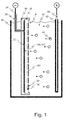
- Fig. 1 shows a device for applying the method according to the invention.
- Fig. 2 shows a semiconductor device according to the invention.
- Fig. 1 shows a device for use and explanation of the method according to the invention. Shown is a tank 50 with a plating bath 52, exemplified by a solution of copper sulfate (CuSO 4 ) in a concentration of the order of 100 grams per liter, in which an electrode 40 is provided, which is connected to the positive pole of a voltage source.
- This electrode 40 serves copper ions (44) to deliver to the electroplating bath 52 and has for this purpose a core of a further metal and a shell 42 of this core with pure copper. It may also be preferred to provide the sheath 42 of a mixture having at least 90% copper content and another metal.
- the respective wafer 8 with the exception of its edge region, forms a two-dimensional matrix of directly adjacent semiconductor components 10.
- the respective semiconductor component 10, in this case the power diode has a p-type conductor extending from its first surface 160, which is simultaneously the first surface of the wafer. doped volume region 16, which is usually formed like a trough and not to the limits 100, see. Fig. 2 , to the next power diode is enough. This surface simultaneously forms the only first contact surface 162 of the respective power diode 10.
- Other semiconductor devices may have a plurality of functionally identical or have different first contact surfaces, however, which are all characterized in that they are assigned to a p-doped volume region 16.
- the rear side that is to say the second surface 140 of the wafer 8 and thus of the semiconductor components 10 has a second contact surface 142.
- this contact surface 142 extends to the boundary 100 of the adjacent power diodes 10, so that, as it were, a continuous contact surface of the wafer 8 is formed.
- the rear side 140 as well as the edge region 18 of the wafer, in some embodiments also the part of the front side 160 directly adjacent to this edge region, are enclosed in a liquid-tight manner by means of a contact device 30.
- This contact device 30 has on its, the rear side 140 of the wafer 8 facing, a contact element 32 which is in electrical contact with the second contact surfaces 142 of all to be coated power diodes 10, regardless of whether they are separated from each other or as here as a common contact surface ,
- the contact device 30 is electrically insulated 36, so that it is not on her a deposition of copper and thus a short circuit of the pn junction over the electroplating bath is avoided.
- the contact device 30 has an external connection element 34, which also leads electrically insulated from the electroplating liquid 52 to the negative pole of the voltage source. Inside the contact device 30, this external connection element 34 is electrically conductively connected to the contact element 32 of the contact device 30.
- the voltage source is to be provided with a voltage of at least 2.5V, preferably between 6V and 8V, since in the context of the method according to the invention the breakdown voltage of the pn junction of typically 0.7V must be overcome by a current flow through the volume-conductive power diode 10 guarantee.
- the copper ions 44 dissolved in the electroplating bath 52 are deposited exclusively on the first contact surfaces 162 of the semiconductor components 10 connected to the p-doped volume regions 16.
- the semiconductor device 10 connected portions of the first surface 160 of the Wafers 8, and the respective semiconductor device 10, no deposition takes place. According to the prior art, these parts of the surface 160 are covered with an insulating layer which serves as a passivation.
- the method allows a deposition rate of between 100 nm / minute and 2000 nm / minute, which by way of example achieves a thickness of the first contact metal layer 20 of 10 ⁇ m after a residence time of 5 to 100 minutes under tension.
- Fig. 2 shows a semiconductor device 10 according to the invention, prepared by the method according to the invention.
- the semiconductor device 10 is again a power diode.
- This has a monocrystalline n-doped main body 12 and a higher n-type doping 14 along the rear side 140. Both regions together form the n-doped volume regions, one of which extends in the edge region of the power diode 10 as far as the first surface 160.
- the second surface 140, the rear side forms the second contact surface 142 of the power diode 10 over its entire surface.
- a third contact metal layer 24, designed as a solderable single or multi-layer contact, is provided here. This third contact metal layer 24 also facilitates electrical contact with the contact element 32 of the contact device 30.
- the p-doped volume region 16 extends like a trough from the first surface 160 into the semiconductor body and forms on the first surface of the first contact surface 162 of the power diode 10 from.
- a thin second contact metal layer 22 is advantageously provided, which mainly serves to improve the adhesion of the first contact metal layer 20, in this case a copper layer with a thickness of 10 ⁇ m.
Landscapes
- Chemical & Material Sciences (AREA)
- Engineering & Computer Science (AREA)
- Chemical Kinetics & Catalysis (AREA)
- Electrochemistry (AREA)
- Materials Engineering (AREA)
- Metallurgy (AREA)
- Organic Chemistry (AREA)
- Life Sciences & Earth Sciences (AREA)
- Sustainable Development (AREA)
- Electrodes Of Semiconductors (AREA)
- Electroplating Methods And Accessories (AREA)
Applications Claiming Priority (1)
| Application Number | Priority Date | Filing Date | Title |
|---|---|---|---|
| DE102011005743A DE102011005743B3 (de) | 2011-03-17 | 2011-03-17 | Verfahren zur Abscheidung einer Metallschicht auf einem Halbleiterbauelement |
Publications (2)
| Publication Number | Publication Date |
|---|---|
| EP2500927A2 true EP2500927A2 (fr) | 2012-09-19 |
| EP2500927A3 EP2500927A3 (fr) | 2014-07-30 |
Family
ID=45566894
Family Applications (1)
| Application Number | Title | Priority Date | Filing Date |
|---|---|---|---|
| EP12154190.8A Withdrawn EP2500927A3 (fr) | 2011-03-17 | 2012-02-07 | Procédé de dépôt d'une couche de métal sur un composant semi-conducteur et composant semi-conducteur |
Country Status (2)
| Country | Link |
|---|---|
| EP (1) | EP2500927A3 (fr) |
| DE (1) | DE102011005743B3 (fr) |
Families Citing this family (1)
| Publication number | Priority date | Publication date | Assignee | Title |
|---|---|---|---|---|
| DE102014105066B3 (de) * | 2014-04-09 | 2015-03-05 | Semikron Elektronik Gmbh & Co. Kg | Verfahren und Vorrichtungen zur Abscheidung einer Metallschicht auf einem Halbleiterbauelement |
Family Cites Families (13)
| Publication number | Priority date | Publication date | Assignee | Title |
|---|---|---|---|---|
| US3013955A (en) * | 1959-04-29 | 1961-12-19 | Fairchild Camera Instr Co | Method of transistor manufacture |
| DE1614982B2 (de) * | 1966-11-09 | 1974-02-21 | Veb Werk Fuer Fernsehelektronik, X 1160 Berlin-Oberschoeneweide | Verfahren zum galvanischen Kontaktieren einer Vielzahl von reihenförmig auf einer Kristallscheibe aus Halbleitermaterial angeordneter Halbleiteranordnungen |
| JPS55118680A (en) * | 1979-03-02 | 1980-09-11 | Motorola Inc | Electrically plating method |
| JPS60128615A (ja) * | 1983-12-15 | 1985-07-09 | Sumitomo Electric Ind Ltd | 半導体ウエハの電解メツキ方法 |
| JP2002520856A (ja) * | 1998-07-08 | 2002-07-09 | シーメンス アクチエンゲゼルシヤフト | 回路装置およびその製造方法 |
| US20040084320A1 (en) * | 2002-10-30 | 2004-05-06 | Xerox Corporation | Copper interconnect by immersion/electroless plating in dual damascene process |
| FR2898138B1 (fr) * | 2006-03-03 | 2008-05-16 | Commissariat Energie Atomique | Procede de structuration electrochimique d'un materiau conducteur ou semi-conducteur, et dispositif de mise en oeuvre. |
| US20070256937A1 (en) * | 2006-05-04 | 2007-11-08 | International Business Machines Corporation | Apparatus and method for electrochemical processing of thin films on resistive substrates |
| DE102007005161B4 (de) * | 2007-01-29 | 2009-04-09 | Nb Technologies Gmbh | Verfahren zur Metallisierung von Substraten |
| US7935621B2 (en) * | 2008-02-15 | 2011-05-03 | International Business Machines Corporation | Anti-fuse device structure and electroplating circuit structure and method |
| US8043966B2 (en) * | 2008-04-11 | 2011-10-25 | International Business Machines Corporation | Method for monitoring patterning integrity of etched openings and forming conductive structures with the openings |
| DE102008028104A1 (de) * | 2008-06-13 | 2009-12-24 | Deutsche Cell Gmbh | Metallisierungsverfahren für Solarzellen |
| DE102009018360A1 (de) * | 2009-04-23 | 2010-11-04 | Rena Gmbh | Verfahren und Vorrichtung zur elektrolytischen Behandlung von Solarzellen |
-
2011
- 2011-03-17 DE DE102011005743A patent/DE102011005743B3/de active Active
-
2012
- 2012-02-07 EP EP12154190.8A patent/EP2500927A3/fr not_active Withdrawn
Non-Patent Citations (1)
| Title |
|---|
| None |
Also Published As
| Publication number | Publication date |
|---|---|
| EP2500927A3 (fr) | 2014-07-30 |
| DE102011005743B3 (de) | 2012-07-26 |
Similar Documents
| Publication | Publication Date | Title |
|---|---|---|
| DE19820878B4 (de) | Verfahren zum Abscheiden einer Materialschicht auf einem Substrat | |
| DE1965546C3 (de) | Halbleiterbauelement | |
| DE102008034164B4 (de) | Modul mit Leistung-Halbleiterchip und Verfahren | |
| DE102019210821B4 (de) | Halbleitervorrichtung und Leistungsumsetzungsvorrichtung | |
| DE112012006610T5 (de) | Solarzelle, Solarzellenmodul und Verfahren zum Fertigen einer Solarzelle | |
| DE112013001641T5 (de) | Solarzelle und Verfahren zum Herstellen einer Solarzelle | |
| DE102014115909B4 (de) | Press-Pack-Zelle und Verfahren zum Betrieb einer Press-Pack-Zelle | |
| EP2162922A1 (fr) | Structure de contact pour un composant semi-conducteur et son procédé de fabrication | |
| EP2087524A2 (fr) | Cellule solaire et module de cellules solaires à électrodes dorsales améliorées et procédé pour leur fabrication | |
| DE102013217802B4 (de) | Halbleiteranordnung, verfahren zur herstellung einer halbleiteranordnung und verfahren zum betrieb einer halbleiteranordnung | |
| DE102015110437A1 (de) | Halbleitervorrichtung mit einer Metallstruktur, die mit einer leitfähigen Struktur elektrisch verbunden ist | |
| DE102004027176B4 (de) | Verfahren zum Herstellen von Halbleiterbauteilen | |
| WO2014079657A1 (fr) | Procédé de réalisation d'une zone de connexion d'une puce de semi-conducteur optoélectronique | |
| DE102011006492B3 (de) | Schottky-Diode und Herstellungsverfahren hierzu | |
| EP2786420A2 (fr) | Cellule solaire et procédé de fabrication d'une cellule solaire | |
| DE102014105066B3 (de) | Verfahren und Vorrichtungen zur Abscheidung einer Metallschicht auf einem Halbleiterbauelement | |
| DE102011005743B3 (de) | Verfahren zur Abscheidung einer Metallschicht auf einem Halbleiterbauelement | |
| DE2348182C3 (de) | Verfahren zur galvanischen Abscheidung einer Metallschicht auf der Oberfläche eines Halbleiterkörpers | |
| DE102008033223A1 (de) | Kontaktstruktur mit selektivem Emitter | |
| DE1952499A1 (de) | Verfahren zum Herstellen eines Halbleiterbauelements | |
| DE102012213555B4 (de) | Verfahren zur Herstellung eines Leistungshalbleitermoduls | |
| WO2015044022A1 (fr) | Procédé de création de motifs sur des couches de matériaux oxydables au moyen de l'oxydation et substrat pourvu d'un tel revêtement à motifs | |
| DE2606885A1 (de) | Halbleiterbauteil | |
| EP2686890A2 (fr) | Procédé de fabrication d'un ensemble de cellules solaires | |
| DE112022006826T5 (de) | Leuchtdiode und Lichtemittierende Vorrichtung |
Legal Events
| Date | Code | Title | Description |
|---|---|---|---|
| PUAI | Public reference made under article 153(3) epc to a published international application that has entered the european phase |
Free format text: ORIGINAL CODE: 0009012 |
|
| AK | Designated contracting states |
Kind code of ref document: A2 Designated state(s): AL AT BE BG CH CY CZ DE DK EE ES FI FR GB GR HR HU IE IS IT LI LT LU LV MC MK MT NL NO PL PT RO RS SE SI SK SM TR |
|
| AX | Request for extension of the european patent |
Extension state: BA ME |
|
| PUAL | Search report despatched |
Free format text: ORIGINAL CODE: 0009013 |
|
| AK | Designated contracting states |
Kind code of ref document: A3 Designated state(s): AL AT BE BG CH CY CZ DE DK EE ES FI FR GB GR HR HU IE IS IT LI LT LU LV MC MK MT NL NO PL PT RO RS SE SI SK SM TR |
|
| AX | Request for extension of the european patent |
Extension state: BA ME |
|
| RIC1 | Information provided on ipc code assigned before grant |
Ipc: C25D 7/12 20060101ALI20140624BHEP Ipc: H01L 21/288 20060101AFI20140624BHEP Ipc: C25D 5/02 20060101ALI20140624BHEP |
|
| STAA | Information on the status of an ep patent application or granted ep patent |
Free format text: STATUS: THE APPLICATION HAS BEEN WITHDRAWN |
|
| 18W | Application withdrawn |
Effective date: 20141113 |