EP2500931B1 - Dispositif à semi-conducteurs, et procédé de fabrication de celui-ci - Google Patents
Dispositif à semi-conducteurs, et procédé de fabrication de celui-ci Download PDFInfo
- Publication number
- EP2500931B1 EP2500931B1 EP10829680.7A EP10829680A EP2500931B1 EP 2500931 B1 EP2500931 B1 EP 2500931B1 EP 10829680 A EP10829680 A EP 10829680A EP 2500931 B1 EP2500931 B1 EP 2500931B1
- Authority
- EP
- European Patent Office
- Prior art keywords
- via hole
- insulating film
- layer
- semiconductor device
- semiconductor substrate
- Prior art date
- Legal status (The legal status is an assumption and is not a legal conclusion. Google has not performed a legal analysis and makes no representation as to the accuracy of the status listed.)
- Active
Links
Images






Classifications
-
- H—ELECTRICITY
- H10—SEMICONDUCTOR DEVICES; ELECTRIC SOLID-STATE DEVICES NOT OTHERWISE PROVIDED FOR
- H10W—GENERIC PACKAGES, INTERCONNECTIONS, CONNECTORS OR OTHER CONSTRUCTIONAL DETAILS OF DEVICES COVERED BY CLASS H10
- H10W20/00—Interconnections in chips, wafers or substrates
- H10W20/01—Manufacture or treatment
- H10W20/021—Manufacture or treatment of interconnections within wafers or substrates
- H10W20/023—Manufacture or treatment of interconnections within wafers or substrates the interconnections being through-semiconductor vias
-
- H—ELECTRICITY
- H10—SEMICONDUCTOR DEVICES; ELECTRIC SOLID-STATE DEVICES NOT OTHERWISE PROVIDED FOR
- H10W—GENERIC PACKAGES, INTERCONNECTIONS, CONNECTORS OR OTHER CONSTRUCTIONAL DETAILS OF DEVICES COVERED BY CLASS H10
- H10W20/00—Interconnections in chips, wafers or substrates
- H10W20/01—Manufacture or treatment
- H10W20/021—Manufacture or treatment of interconnections within wafers or substrates
- H10W20/023—Manufacture or treatment of interconnections within wafers or substrates the interconnections being through-semiconductor vias
- H10W20/0234—Manufacture or treatment of interconnections within wafers or substrates the interconnections being through-semiconductor vias comprising etching via holes that stop on pads or on electrodes
-
- H—ELECTRICITY
- H10—SEMICONDUCTOR DEVICES; ELECTRIC SOLID-STATE DEVICES NOT OTHERWISE PROVIDED FOR
- H10W—GENERIC PACKAGES, INTERCONNECTIONS, CONNECTORS OR OTHER CONSTRUCTIONAL DETAILS OF DEVICES COVERED BY CLASS H10
- H10W20/00—Interconnections in chips, wafers or substrates
- H10W20/01—Manufacture or treatment
- H10W20/021—Manufacture or treatment of interconnections within wafers or substrates
- H10W20/023—Manufacture or treatment of interconnections within wafers or substrates the interconnections being through-semiconductor vias
- H10W20/0242—Manufacture or treatment of interconnections within wafers or substrates the interconnections being through-semiconductor vias comprising etching via holes from the back sides of the chips, wafers or substrates
-
- H—ELECTRICITY
- H10—SEMICONDUCTOR DEVICES; ELECTRIC SOLID-STATE DEVICES NOT OTHERWISE PROVIDED FOR
- H10W—GENERIC PACKAGES, INTERCONNECTIONS, CONNECTORS OR OTHER CONSTRUCTIONAL DETAILS OF DEVICES COVERED BY CLASS H10
- H10W20/00—Interconnections in chips, wafers or substrates
- H10W20/20—Interconnections within wafers or substrates, e.g. through-silicon vias [TSV]
-
- H—ELECTRICITY
- H10—SEMICONDUCTOR DEVICES; ELECTRIC SOLID-STATE DEVICES NOT OTHERWISE PROVIDED FOR
- H10W—GENERIC PACKAGES, INTERCONNECTIONS, CONNECTORS OR OTHER CONSTRUCTIONAL DETAILS OF DEVICES COVERED BY CLASS H10
- H10W70/00—Package substrates; Interposers; Redistribution layers [RDL]
- H10W70/60—Insulating or insulated package substrates; Interposers; Redistribution layers
- H10W70/62—Insulating or insulated package substrates; Interposers; Redistribution layers characterised by their interconnections
- H10W70/65—Shapes or dispositions of interconnections
-
- H—ELECTRICITY
- H10—SEMICONDUCTOR DEVICES; ELECTRIC SOLID-STATE DEVICES NOT OTHERWISE PROVIDED FOR
- H10W—GENERIC PACKAGES, INTERCONNECTIONS, CONNECTORS OR OTHER CONSTRUCTIONAL DETAILS OF DEVICES COVERED BY CLASS H10
- H10W72/00—Interconnections or connectors in packages
- H10W72/01—Manufacture or treatment
- H10W72/019—Manufacture or treatment of bond pads
-
- H—ELECTRICITY
- H10—SEMICONDUCTOR DEVICES; ELECTRIC SOLID-STATE DEVICES NOT OTHERWISE PROVIDED FOR
- H10W—GENERIC PACKAGES, INTERCONNECTIONS, CONNECTORS OR OTHER CONSTRUCTIONAL DETAILS OF DEVICES COVERED BY CLASS H10
- H10W72/00—Interconnections or connectors in packages
- H10W72/20—Bump connectors, e.g. solder bumps or copper pillars; Dummy bumps; Thermal bumps
- H10W72/29—Bond pads specially adapted therefor
-
- H—ELECTRICITY
- H10—SEMICONDUCTOR DEVICES; ELECTRIC SOLID-STATE DEVICES NOT OTHERWISE PROVIDED FOR
- H10W—GENERIC PACKAGES, INTERCONNECTIONS, CONNECTORS OR OTHER CONSTRUCTIONAL DETAILS OF DEVICES COVERED BY CLASS H10
- H10W72/00—Interconnections or connectors in packages
- H10W72/90—Bond pads, in general
- H10W72/921—Structures or relative sizes of bond pads
- H10W72/922—Bond pads being integral with underlying chip-level interconnections
Definitions
- the present invention relates to a semiconductor device having a through-hole electrode layer formed in a semiconductor substrate, and a manufacturing method of the semiconductor device.
- miniaturization is demanded of a package (a semiconductor device) in an integrated circuit used in an electronic device.
- a through-hole electrode penetrating through a semiconductor substrate is replacing conventional wire bonding.
- Fig. 17 is a cross-sectional view showing one example of a conventional semiconductor device.
- a semiconductor device 101 is substantially structured with a semiconductor substrate 102made of silicon or the like, a via hole 107, a second oxide film 109, a barrier layer 110, and a rewiring layer 111.
- the via hole 107 extends from a back surface 102b of the semiconductor substrate 102 to reach a pad electrode 105.
- the second oxide film 109 is formed on the sidewall of the via hole 107 and on the back surface 102b of the semiconductor substrate 102.
- the barrier layer 110 and the rewiring layer 111 are formed inside the via hole 107 and on the back surface 102b of the semiconductor substrate 102.
- Fig. 18 is a flowchart showing a manufacturing method of the conventional semiconductor device.
- Figs. 19 to 26 are each a cross-sectional view showing the state at each step in the manufacturing method of the conventional semiconductor device.
- a first oxide film 106 on a front surface 102a of the semiconductor substrate 102 where a circuit (not shown) is formed the pad electrode 105 and a passivation film 104 are formed. Thereafter, on the passivation film 104, a supporting substrate 103 is attached through an adhesive (not shown) (step S101 in Fig. 18 ).
- a resist 112 is formed for providing an opening at a position corresponding to the pad electrode 105 (step S102 in Fig. 18 ).
- the via hole 107 reaching the first oxide film 106 is formed (step S103 in Fig. 18 ).
- step S104 in Fig. 18 by etching the first oxide film 106 using the resist 112 as an etching-purpose mask, the via hole 107 reaching the pad electrode 105 is formed (step S104 in Fig. 18 ).
- step S105 in Fig. 18 the resist 112 on the back surface 102b of the semiconductor substrate 102 is removed therefrom.
- the second oxide film 109 is formed inside the via hole 107 and on the back surface 102b of the semiconductor substrate 102 (step S106 in Fig. 18 ) .
- step S107 in Fig. 18 by etching the second oxide film 109 at the bottom of the via hole 107, the pad electrode 105 is exposed again (step S107 in Fig. 18 ).
- the barrier layer 110 and the rewiring layer 111 are formed on the second oxide film 109 in order (step S108 in Fig. 18 ).
- the pad electrode 105 is electrically connected to the back surface 102b of the semiconductor substrate 102 through a through-hole electrode 108 which is structured with the barrier layer 110 and the rewiring layer 111.
- the pad electrode 105 and the through-hole electrode 108 contact each other by a contact area corresponding to a diameter of the via hole 107.
- the resistance value between the pad electrode 105 and the through-hole electrode 108 is determined by the contact area (for example, see Patent Literature 1).
- the diameter of the via hole 107 must be reduced accordingly. As a result, the aspect ratio of the via hole 107 is increased, and the manufacturing cost increases.
- WO 2009/115449 discloses a method of forming a TSV from the backside of a silicon substrate and landing on a plurality of contacts.
- a silicide may be formed between the contacts and the TSV.
- US 2006/0033168 discloses another method of forming a TSV from the substrate backside and landing on the extension of a pad electrode.
- the extension may optionally include a barrier layer.
- JP 2006128352 discloses yet another method of forming a TSV landing on a lower pad electrode formed under an upper pad electrode.
- Patent Literature 1 Japanese Unexamined Patent Publication No. 2005-235860
- the resistance value between the pad electrode 105 and the through-hole electrode 108 is dependent on the diameter of the via hole 107. Accordingly, it involves such an issue that the variations in diameter of the via hole 107 invite fluctuations in the resistance value between the pad electrode 105 and the through-hole electrode 108.
- the present invention resolves the conventional issue, and an object thereof is to provide a highly reliable semiconductor device, and a manufacturing method of the semiconductor device, in which the resistance value between the padelectrode and the through-hole electrode layer is independent of the variations in diameter of the via hole, and variations in resistance value are small.
- the present invention is structured as follows.
- a semiconductor device is characterized in comprising:
- the resistance value between the pad electrode and the through-hole electrode layer is independent of variations in diameter or in the width of the via hole. Therefore, a highly reliable semiconductor device with small variations in resistance value, and a manufacturing method of the semiconductor device can be provided.
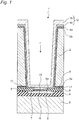
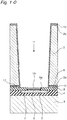
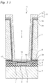
- Fig. 1 is a cross-sectional view of a semiconductor device according to a first embodiment of the present invention.
- a semiconductor device 1 is structured to include a semiconductor substrate 2, a pad electrode 5, a contact electrode 6, a first oxide film 8, a second oxide film 9, a third oxide film 13, a silicide portion 10, a via hole 11, a first barrier layer 7, a second barrier layer 14, and a rewiring layer 15.
- the contact electrode 6 is one example of an electrode section, and has an external connection terminal.
- the second oxide film 9 is one example of a first insulating film.
- the third oxide film 13 is one example of a second insulating film.
- the silicide portion 10 is one example of a silicide layer.
- the second barrier layer 14 and the rewiring layer 15 structure a through-hole electrode layer 12.
- the second oxide film 9 is formed on the first oxide film 8 that is formed on a front surface 2a of the semiconductor substrate 2. Further, the contact electrode 6 is disposed in a circular hole 9a provided at the second oxide film 9, and is electrically connected to the pad electrode 5 that is provided on the second oxide film 9.
- the first barrier layer 7 covers the contact electrode 6 so as to enhance adhesion of the second oxide film 9 and the contact electrode 6.
- the silicide portion 10 is disposed in the circular hole 9a provided at the second oxide film 9 so as to be electrically connected to the first barrier layer 7 covering the contact electrode 6, and is formed between the contact electrode 6 and the through-hole electrode layer 12.
- the via hole 11 is formed to extend from a back surface 2b of the semiconductor substrate 2 to reach the silicide portion 10 and the second oxide film 9.
- the third oxide film 13 is formed on the sidewall of the via hole 11 and on the back surface 2b of the semiconductor substrate 2.
- the second barrier layer 14 and the rewiring layer 15 are formed inside the via hole 11 (i.e., on the sidewall and on the bottom surface) and on the back surface 2b of the semiconductor substrate 2 in order.
- the second barrier layer 14 contacts the silicide portion 10 to establish an electrical connection therebetween.
- the pad electrode 5 and the through-hole electrode layer 12 are electrically connected to each other via the contact electrode 6, the first barrier layer 7, and the silicide portion 10. Further, the pad electrode 5 and the through-hole electrode layer 12 are electrically insulated by the second oxide film 9 at the portion where the contact electrode 6, the first barrier layer 7, and the silicide portion 10 are not interposed.
- the semiconductor substrate 2 and the through-hole electrode layer 12 are electrically insulated by the third oxide film 13 formed on the sidewall of the via hole 11 and on the back surface 2b of the semiconductor substrate 2.
- any materials which exhibit low resistance between the pad electrode 5 and the contact electrode 6 will suffice.
- the pad electrode 5 aluminum, copper or an alloy thereof, titanium, titanium nitride, tantalum, tantalum nitride, a high melting point metal, or a compound thereof, or the like is used.
- used as the contact electrode 6 is tungsten, aluminum or an alloy thereof, copper, or the like.
- the contact electrode 6 may be of a single contact form, or may be of a form structured with a plurality of contacts as shown in Figs . 15 and 16 .
- the diameter of the contact electrode 6 may be as great as or greater than the diameter of the pad electrode 5.
- first barrier layer 7 for the purpose of enhancing adhesion of the second oxide film 9 and the contact electrode 6, titanium, titanium nitride, titanium tungsten, tantalum, tantalumnitride, ahighmeltingpointmetal, or a lamination film made up thereof, or the like.
- silicide portion 10 which is formed on the front surface 2a of the semiconductor substrate 2, for the purpose of reducing the resistance, there is used tungsten silicide, titanium silicide, cobalt silicide, nickel silicide, or the like.
- Used as the second barrier layer 14 is, for the purpose of enhancing adhesion of the silicide portion 10 and the rewiring layer 15, titanium, titanium nitride, titanium tungsten, tantalum, tantalumnitride, ahighmeltingpointmetal, or a lamination film made up thereof, or the like.
- the first oxide film 8 and the second oxide film 9 there is used SiO 2 , an oxynitride film, a nitride film, or the like.
- the material for the supporting substrate 3 is silicon glass.
- the supporting substrate 3 is attached to the passivation film 4, through an adhesive or by joining.
- a diameter A of the silicide portion 10 is adjusted such that the following relationship of (Expression 1) is established between itself and a diameter B of the via hole 11. Then, the silicide portion 10 is formed with the diameter A of the silicide portion 10 adjusted in this manner. It is to be noted that, in a case where the silicide portion 10 and the via hole 11 are both in a circular shape, the comparison is based on their diameters; in a case where the silicide portion 10 and the via hole 11 are both in a quadrilateral shape, the comparison is based on their width dimensions.
- the reason why the condition of the above-stated (Expression 1) is defined is to reduce variations in resistance value of the through-hole electrode layer 12.
- the diameter A of the silicide portion 10 whose shape is uniquely determined makes it possible to define the resistance value of the through-hole electrode layer 12, and to reduce the variations in resistance value of the through-hole electrode layer 12.
- the resistance value is defined by the diameter B of the via hole 11
- the shape of the via hole 11 of the through-hole electrode obtained by etching may possibly vary.
- the variations in resistance value of the through-hole electrode may possibly occur.
- the thickness of the second barrier layer 14 on the bottom surface of the via hole 11 is uniform. Accordingly, in the first embodiment, the bottom surface of the via hole 11 is in a flat shape.
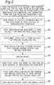
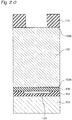
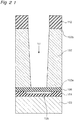
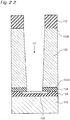
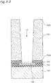
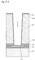
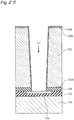
- FIG. 2 is a flowchart showing the manufacturing method of the semiconductor device according to the first embodiment of the present invention.
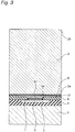
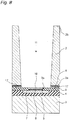
- Figs. 3 to 11 are each a cross-sectional view showing the manufacturing method of the semiconductor device according to the first embodiment of the present invention.
- the first oxide film 8 is formed on the front surface 2a of the semiconductor substrate 2 where a circuit (not shown) is formed.
- the second oxide film 9 and a polysilicon film 17 are formed on the first oxide film 8 and in the circular hole 9a of the second oxide film 9.
- the pad electrode 5 is formed on the second oxide film 9 and the contact electrode 6, and the passivation film 4 is formed on the second oxide film 9 and the pad electrode 5 (step S1 in Fig. 2 ).
- the silicide portion 10, the first barrier layer 7, and the contact electrode 6 are disposed in the circular hole 9a that is provided at the second oxide film 9.
- the first oxide film 8 is thick enough to electrically insulate the semiconductor substrate 2 and the polysilicon film 17 from each other.
- the pad electrode 5 is electrically connected to the polysilicon film 17 via the silicide portion 10, the first barrier layer 7, and the contact electrode 6. Further, because the semiconductor substrate 2 and the polysilicon film 17 are electrically insulated from each other, the pad electrode 5 is electrically insulated from the semiconductor substrate 2. Accordingly, using a measuring terminal or the like to probe the pad electrode 5, in a state before the via hole 11 is formed as shown in Fig. 3 , using the electrode section (specifically, by establishing an electrical connection among the silicide portion 10, the first barrier layer 7, and the contact electrode 6 via the pad electrode 5), it becomes possible to measure the electrical characteristic of the circuit formed on the semiconductor substrate 2. This makes it possible to determine whether the circuit of the semiconductor substrate 2 is acceptable or defective, before the semiconductor device 1 is completed.
- a diameter C of the polysilicon film 17 is set such that the following relationship of (Expression 2) is established between itself and the diameter A of the silicide portion10. It is to be noted that, in a case where the polysilicon film 17 and the silicide portion 10 are both circular, the comparison is based on their diameters; in a case where the polysilicon film 17 and the silicide portion 10 are both quadrilateral, the comparison is based on their width dimensions . C ⁇ A
- the reason why the condition of the above-stated (Expression 2) is defined is to further reduce the variations in resistance value of the through-hole electrode layer 12.
- the diameter A of the silicide portion 10 whose shape is uniquely determined makes it possible to define the resistance value of the through-hole electrode layer 12, and to reduce the variations in resistance value of the through-hole electrode layer 12.
- the shape of the polysilicon film 17 may possibly vary.
- the variations in resistance value of the through-hole electrode may possibly occur.
- the silicide portion 10 a layer formed through a thermal reaction of the first barrier layer 7 is used.
- the silicide portion 10 a layer made of tungsten silicide, titanium silicide, cobalt silicide, nickel silicide, or the like, which is formed through a thermal reaction after another film (e.g., made of tungsten, titanium, cobalt, nickel, or the like) is deposited on the polysilicon film 17.
- another film e.g., made of tungsten, titanium, cobalt, nickel, or the like
- the diameter of the silicide portion 10 is equal to the hole diameter of the contact electrode 6.
- the supporting substrate 3 is attached through an adhesive (not shown).
- a resist 16 having an opening portion 16a is formed for providing an opening at a position corresponding to the pad electrode 5 (step S2 in Fig. 2 ).
- the via hole 11 reaching the first oxide film 8 is formed (step S3 in Fig. 2 ).
- the first oxide film 8 serves as an etching stopper layer for the semiconductor substrate 2, and the shape of the bottom surface of the via hole 11 becomes flat.
- the diameter B of the via hole 11 is adjusted such that the above-stated relationship of (Expression 1) is established between itself and the diameter A of the silicide portion 10. It is to be noted that, from the viewpoint of the adhesion of the second barrier layer 14, the diameter B of the via hole 11 is desirably equal to or less than the diameter C of the polysilicon film 17. However, so long as it falls within the range in which the above-stated relationship of (Expression 2) is satisfied, the diameter B of the via hole 11 may be greater than the diameter C of the polysilicon film 17.
- the via hole 11 reaching the polysilicon film 17 is formed (step S4 in Fig. 2 ).
- the polysilicon film 17 serves as an etching stopper layer of the first oxide film 8, and the shape of the bottom surface of the via hole 11 becomes flat.
- the via hole 11 reaching the silicide portion 10 and the second oxide film 9 is formed (step S5 in Fig. 2 ).
- the silicide portion 10 and the second oxide film 9 each serve as an etching stopper layer for the polysilicon film 17, and the shape of the bottom surface of the via hole 11 becomes flat.
- the etching of the polysilicon film 17 is desirably carried out by dry etching.
- the etching of the polysilicon film 17 is not necessary.
- the polysilicon film 17 in this case has its resistance reduced by doping. While n-type doping is desirable, it may be of the p-type. However, in a case where the polysilicon film 17 is used as part of the electrode as it is, the polysilicon film 17 may not be etched. In that case, it is desirable that the polysilicon film 17 is doped.
- the resist 16 is removed from the back surface 2b of the semiconductor substrate 2 (step S6 in Fig. 2 ).
- wet processing or dry processing is used for carrying out the removal of the resist 16.
- the third oxide film 13 is formed (step S7 in Fig. 2 ).
- thermal oxidation, CVD, or sputtering is used.
- the silicide portion 10 and the second oxide film 9 are exposed again (step S8 in Fig. 2 ).
- the third oxide film 13 is desirably carried out by dry etching.
- the third oxide film 13 on the sidewall of the via hole 11 and on the back surface 2b of the semiconductor substrate 2 just slightly reduces in thickness and remains mostly.
- the secondbarrier layer 14 and the rewiring layer 15 are formed on the third oxide film 13 (step S9 in Fig. 2 ).
- CVD or sputtering is used. Because the shape of the bottom surface of the via hole 11 is flat, the thickness of the second barrier layer 14 on the bottom surface of the via hole 11 becomes uniform, and the second barrier layer 14 which exhibits excellent adhesion to the third oxide film 13 is formed. Further, the second barrier layer 14 on the bottom surface of the via hole 11 suppresses diffusion of the material structuring the rewiring layer 15 (e.g., Cu) into the semiconductor substrate 2.
- the material structuring the rewiring layer 15 e.g., Cu
- the second barrier layer 14 can be thinned.
- the rewiring layer 15 is formed by plating, while the rewiring layer 15 may be formed by CVD, sputtering, or any combination thereof.
- the rewiring layer 15 is shaped such that the via hole 11 is buried incompletely (i.e., partially) or buried completely (i.e., entirely).
- the resistance value between the pad electrode 5 and the through-hole electrode layer 12 is dependent on the diameter of the silicide portion 10, and not on the diameter of the via hole 11. Accordingly, the resistance value between the pad electrode 5 and the through-hole electrode layer 12 will not be affected by the variations in diameter of the via hole 11.
- the via hole 11 and the silicide portion 10 are different in processing accuracy.
- the processing variation in diameter of the via hole 11 is approximately 1 ⁇ m, whereas the processing variation in diameter of the silicide portion 10 is approximately 1 nm. Accordingly, with the semiconductor device 1 and the manufacturing method thereof according to the first embodiment, the variations in resistance value between the pad electrode 5 and the through-hole electrode layer 12 can be reduced as compared to the conventional manner.
- the diameter of the via hole 11 can be set to be greater than the diameter of the pad electrode 5. Therefore, the aspect ratio of the via hole 11 can be reduced, thereby to reduce the manufacturing cost. Furthermore, a reduction in size of the pad electrode 5 makes it possible to reduce the area of the semiconductor chip.
- the shape of the bottom surface of the via hole 11 becomes flat. This allows the thickness of the second barrier layer 14 on the bottom surface of the via hole 11 to be uniform. Because the thickness of the second barrier layer 14 on the bottom surface of the via hole 11 becomes uniform, the second barrier layer 14 exhibiting excellent adhesion to the third oxide film 13 can be formed.
- Fig. 15 is a cross-sectional view of a semiconductor device of a first example according to the first embodiment, in which the contact electrode 6 is structured with a plurality of disc-like or quadrilateral plate-like contact members 6b in the second oxide film 9.
- the contact electrode 6 is structured with a plurality of disc-like or quadrilateral plate-like contact members 6b in the second oxide film 9.
- one silicide portion 10 is formed in one hole 9d at the second oxide film 9.
- the plurality of disc-like or quadrilateral plate-like contact members 6b are disposed in a plurality of small holes 9b at the second oxide film 9. It is to be noted that, at this time, the plurality of disc-like or quadrilateral plate-like contact members 6b are disposed so as to each contact the silicide portion 10.
- Fig. 16 is a cross-sectional view of a semiconductor device of a second example according to the first embodiment, in which the contact electrode 6 is structured with a plurality of disc-like or quadrilateral plate-like contact members 6c in the second oxide film 9.
- the contact electrodes 6c are respectively formed in a plurality of holes 9c at the second oxide film 9.
- silicide portions 10c are formed in the holes 9c, respectively. It is to be noted that, at this time, the silicide portions 10c are formed so as to contact the contact electrodes 6c in the plurality of holes 9c, respectively.
- the resistance value between the pad electrode 5 and the through-hole electrode layer 12 is independent of the variations in diameter of the via hole 11. Accordingly, the semiconductor device having the structure shown in Figs. 15 and 16 is also highly reliable with small variations in resistance value.
- the first barrier layer 7 and the contact electrode 6 are separately formed.
- the present invention is not limited thereto.
- the first barrier layer 7 and the contact electrode 6 may integrally be formed as a contact electrode 6A. That is, the first barrier layer 7 may be thinned or may be omitted.
- a laminated film in which a TiN layer and a Ti layer are laminated is used as one example of the first barrier layer 7.
- the Ti layer of the first barrier layer 7 has a function of forming an ohmic contact with the polysilicon film 17, and a function of improving adhesion of the second oxide film 9 to the TiN layer of the first barrier layer 7.
- the ohmic contact for example, by forming the silicide portion 10 of TiSi 2 by a thermal reaction between Ti of the Ti layer and Si of the polysilicon film 17, the ohmic contact can be obtained. It is to be noted that, in a case where the silicide portion 10 is formed at a portion other than the first barrier layer 7, the Ti layer can be omitted.
- any contact electrode material that does not diffuse into the polysilicon film 17 and the semiconductor substrate 2 can be used in the contact electrode 6, the TiN layer of the first barrier layer 7 becomes unnecessary.
- the first barrier layer 7 can be structured solely with the TiN layer, while omitting the Ti layer. Further, use of any contact electrode material that does not diffuse into the semiconductor substrate 2 and the polysilicon film 17 and that possesses excellent adhesion force, in the contact electrode 6 makes it possible to omit the TiN layer of the first barrier layer 7, such that the first barrier layer 7 can be formed solely with the Ti layer.
- the contact electrode 6 solely can be formed as the contact electrode 6A, without the necessity of forming the first barrier layer 7 itself.
- the first barrier layer 7, the contact electrode 6, and the pad electrode 5 are separately formed.
- the present invention is not limited thereto.
- the first barrier layer 7, the contact electrode 6, and the pad electrode 5 may be integrated so as to be formed as a single pad electrode 5A. Because integration of the first barrier layer 7 and the contact electrode 6 is the same as that of the first modified example, description will chiefly be given of the integration of the contact electrode 6 and the pad electrode 5.
- the contact electrode 6 is connected to the polysilicon film 17 and the pad electrode 5 at low resistance.
- the pad electrode 5 is connected to the contact electrode 6 at low resistance. They are necessary from the viewpoint of securing a flat portion when wire bonding is carried out. That is, provision of the pad electrode 5 separately from the contact electrode 6 makes it possible to improve flatness, as compared to a case where the contact electrode 6 solely is employed as an external electrode terminal.
- the contact electrode 6 and the pad electrode 5 are connected to the polysilicon film 17 at low resistance (in other words, when the contact electrode 6 and the pad electrode 5 are integrated so as to form the pad electrode 5A as in the second modified example), as shown in Fig. 13 , it becomes possible to form a flat plane, forming a vertical cross section of the pad electrode 5A into a convex shape. Further, in a case where wire bonding is not used, the pad electrode 5A is not necessarily flat.
- the first barrier layer 7, the contact electrode 6, and the pad electrode 5 are separately formed as one resolution to the aforementioned issue in the manufacturing method. Therefore, in a case where such an issue can be resolved, it is also possible to form the pad electrode 5A by integrating the first barrier layer 7, the contact electrode 6, and the pad electrode 5 as in the second modified example.
- the second barrier layer 14 and the rewiring layer 15 are separately formed.
- the present invention is not limited thereto .
- the second barrier layer 14 and the rewiring layer 15 may be integrated so as to be formed as a rewiring layer 15A.
- Fig. 14 shows an application of the third modified example to the second modified example shown in Fig. 13
- the present invention is not limited thereto.
- the third modified example can be also applied to the first modified example.
- the second barrier layer 14 (e.g., the layer structured with Ti) has a function of preventing diffusion of the rewiring layer 15 into the semiconductor substrate 2 and the polysilicon film 17, and a function of improving adhesion force of the third oxide film 13 and the rewiring layer 15.
- the rewiring layer 15 (e.g., the layer structured with Cu) is low resistant, and has a function of bearing a solder ball. It is to be noted that, so long as it is possible to use as the rewiring layer 15 a rewiring material that can possess the function of preventing diffusion into the semiconductor substrate 2 and the polysilicon film 17 and that exhibits excellent adhesion force, similarly to the third modified example, as shown in Fig. 14 , the rewiring layer 15 can be formed as the rewiring layer 15 solely, while omitting the second barrier layer 14.
- the second barrier layer 14 and the rewiring layer 15 are separately formed as one resolution to the aforementioned issue in the manufacturing method. Therefore, in a case where such an issue can be resolved, it is also possible to form the rewiring layer 15A by integrating the second barrier layer 14 and the rewiring layer 15 as in the third modified example.
- the semiconductor substrate 2 is made of a material such as silicon, and it may be electrically conductive, insulating, or semi-insulating.
- the polysilicon film 17 may remain in the final product in some cases depending on a manufacturing method which will be described later, but may not remain in the final product in other cases.
- the polysilicon film 17 is formed desirably before the second oxide film 9 is formed. Alternatively, the polysilicon film 17 may be formed after the second oxide film 9 is formed.
- the semiconductor device and the semiconductor device manufacturing method of the present invention provide a through-hole electrode layer whose variations in resistance value are small.
- the present invention can be widely applied to a semiconductor device in which a through-hole electrode layer is formed in a semiconductor substrate, and to a manufacturing method of the semiconductor device.
Landscapes
- Internal Circuitry In Semiconductor Integrated Circuit Devices (AREA)
Claims (9)
- Procédé de fabrication d'un dispositif à semi-conducteur, comprenant de :former (S1) un premier film isolant (9) sur une surface avant (2a) d'un substrat semi-conducteur (2) ;former (S1) une électrode de contact (6) dans le premier film isolant (9) ;former (S1) une couche barrière (7) qui recouvre l'électrode de contact (6) ;former (S1) une couche de siliciure (10) qui est connectée à l'électrode de contact (6), dans le premier film isolant (9) ;former ensuite (S3, S4, S5) un trou traversant (11) vers la surface avant (2a) à partir d'une surface arrière (2b) du substrat semi-conducteur (2) par gravure, tandis que le premier film isolant (9) et la couche de siliciure (10) servent de couches d'arrêt de gravure ;former (S7) un second film isolant (13) sur une paroi latérale et une surface inférieure du trou traversant (11) et sur la surface arrière (2b) du substrat semi-conducteur (2) ;graver (S8) le second film isolant (13) pour exposer la couche de siliciure (10) et le premier film isolant (9) dans le trou traversant (11) ; etformer (S9) une couche d'électrode de trou traversant (12) au niveau du second film isolant (13) sur la paroi latérale du trou traversant (11), du second film isolant (13) sur la surface arrière (2b) du substrat semi-conducteur (2), du premier film isolant (9) sur la surface inférieure du trou traversant (11), et de couche de siliciure (10),dans lequelune relation entre une largeur A de la couche de siliciure (10) et une largeur B d'un fond du trou traversant (11) dans une section transversale prise le long d'un plan comprenant un axe central du trou traversant (11) satisfait A ≤ B.
- Procédé de fabrication d'un dispositif à semi-conducteur selon la revendication 1, comprenant en outre de :
avant de former la couche d'électrode de trou traversant (12), mesurer une caractéristique électrique d'un circuit formé au niveau du substrat semi-conducteur (2) en utilisant l'électrode de contact (6). - Dispositif à semi-conducteur (1) comprenant :un premier film isolant (9) qui est formé sur une surface avant (2a) d'un substrat semi-conducteur (2) ;une électrode de contact (6) qui est formée dans le premier film isolant (9) et qui est recouverte d'une couche barrière (7) ;un trou traversant pénétrant dans la surface avant à partir d'une surface arrière du substrat semi-conducteur ;un second film isolant (13) qui est formé sur une paroi latérale du trou traversant (11) et sur la surface arrière (2b) du substrat semi-conducteur (2) ;une couche d'électrode de trou traversant (12) formée au niveau du second film isolant (13) sur la paroi latérale du trou traversant (11), du second film isolant (13) sur la surface arrière (2b) du substrat semi-conducteur (2), et du premier film isolant (9) sur la surface inférieure (2a) du trou traversant (11) ; etune couche de siliciure (10) qui est formée dans le premier film isolant (9) et entre l'électrode de contact (6) et la couche d'électrode de trou traversant (12), et qui est connectée à l'électrode de contact (6) et à la couche d'électrode de trou traversant (12), dans lequelune relation entre une largeur A de la couche de siliciure (10) et une largeur B d'un fond du trou traversant (11) dans une section transversale prise dans un plan comprenant un axe central du trou traversant (11) satisfait A ≤ B.
- Dispositif à semi-conducteur (1) selon la revendication 3, dans lequel
une forme d'une surface inférieure de la couche d'électrode de trou traversant (12) connectée électriquement à l'électrode de contact (6) via la couche de siliciure (10) est plate. - Dispositif à semi-conducteur (1) selon l'une quelconque des revendications 3 et 4, dans lequel
un film de polysilicium (17) est formé entre la surface avant (2a) du substrat semi-conducteur (2) et le premier film isolant (9), et
une relation entre un diamètre C du polysilicium et un diamètre A de la couche de siliciure (10) dans une section transversale prise le long d'un plan incluant l'axe central du trou traversant (11) satisfait C ≥ A. - Dispositif à semi-conducteur (1) selon l'une quelconque des revendications 3 et 4, dans lequel
le premier film isolant (9) est l'un parmi un film de SiO2, un film d'oxynitrure, ou un film de nitrure. - Dispositif à semi-conducteur (1) selon la revendication 3, dans lequel
l'un d'un film de polysilicium (17) et d'un film de silicium amorphe est formé entre la surface avant (2a) du substrat semi-conducteur (2) et le premier film isolant (9). - Dispositif à semi-conducteur (1) selon l'une quelconque des revendications 3 et 4, dans lequel
la couche de siliciure (10) est constituée de l'un quelconque parmi le siliciure de tungstène, le siliciure de titane, le siliciure de cobalt, et le siliciure de nickel. - Dispositif à semi-conducteur (1) selon l'une quelconque des revendications 3 et 4, dans lequel
la couche barrière (7) est constituée de l'un quelconque parmi le titane, le nitrure de titane, le tungstène de titane, le tantale, le nitrure de tantale, un métal à point de fusion élevé, et un film stratifié constitué de ceux-ci.
Applications Claiming Priority (2)
| Application Number | Priority Date | Filing Date | Title |
|---|---|---|---|
| JP2009258582 | 2009-11-12 | ||
| PCT/JP2010/006426 WO2011058712A1 (fr) | 2009-11-12 | 2010-11-01 | Dispositif à semi-conducteurs, et procédé de fabrication de celui-ci |
Publications (3)
| Publication Number | Publication Date |
|---|---|
| EP2500931A1 EP2500931A1 (fr) | 2012-09-19 |
| EP2500931A4 EP2500931A4 (fr) | 2014-03-26 |
| EP2500931B1 true EP2500931B1 (fr) | 2018-10-24 |
Family
ID=43991386
Family Applications (1)
| Application Number | Title | Priority Date | Filing Date |
|---|---|---|---|
| EP10829680.7A Active EP2500931B1 (fr) | 2009-11-12 | 2010-11-01 | Dispositif à semi-conducteurs, et procédé de fabrication de celui-ci |
Country Status (5)
| Country | Link |
|---|---|
| US (1) | US8471367B2 (fr) |
| EP (1) | EP2500931B1 (fr) |
| JP (1) | JP5518091B2 (fr) |
| CN (1) | CN102282656B (fr) |
| WO (1) | WO2011058712A1 (fr) |
Families Citing this family (17)
| Publication number | Priority date | Publication date | Assignee | Title |
|---|---|---|---|---|
| JP5754239B2 (ja) * | 2011-05-24 | 2015-07-29 | ソニー株式会社 | 半導体装置 |
| JP6026756B2 (ja) * | 2012-03-06 | 2016-11-16 | 日本電信電話株式会社 | 半導体装置の製造方法 |
| JP5925006B2 (ja) | 2012-03-26 | 2016-05-25 | ルネサスエレクトロニクス株式会社 | 半導体集積回路装置の製造方法 |
| JP5984134B2 (ja) * | 2012-05-15 | 2016-09-06 | ローム株式会社 | 半導体装置およびその製造方法、電子部品 |
| JP6034747B2 (ja) * | 2013-02-21 | 2016-11-30 | 株式会社東芝 | 半導体装置およびその製造方法 |
| US9764153B2 (en) * | 2013-03-14 | 2017-09-19 | Taiwan Semiconductor Manufacturing Company, Ltd. | Interconnect structure and method of forming same |
| CN104617035A (zh) * | 2013-11-05 | 2015-05-13 | 中芯国际集成电路制造(上海)有限公司 | 半导体器件的形成方法 |
| TWI581325B (zh) * | 2014-11-12 | 2017-05-01 | 精材科技股份有限公司 | 晶片封裝體及其製造方法 |
| JP2016115698A (ja) * | 2014-12-11 | 2016-06-23 | トヨタ自動車株式会社 | 半導体装置とその製造方法 |
| EP3312874A1 (fr) * | 2016-10-20 | 2018-04-25 | ams AG | Procédé de formation d'un trou métallisé à travers un substrat et dispositif à semi-conducteurs comprenant un trou métallisé à travers un substrat |
| US10115579B2 (en) * | 2016-11-30 | 2018-10-30 | Asm Technology Singapore Pte Ltd | Method for manufacturing wafer-level semiconductor packages |
| JP2018157110A (ja) * | 2017-03-17 | 2018-10-04 | 東芝メモリ株式会社 | 半導体装置およびその製造方法 |
| JP2019067937A (ja) * | 2017-10-02 | 2019-04-25 | ソニーセミコンダクタソリューションズ株式会社 | 半導体装置、半導体装置の製造方法、及び、電子機器 |
| EP3550600B1 (fr) | 2018-04-04 | 2020-08-05 | ams AG | Procédé de formation d'un trou métallisé à travers un substrat et dispositif à semi-conducteurs comprenant le trou métallisé |
| KR102521658B1 (ko) | 2018-09-03 | 2023-04-13 | 삼성전자주식회사 | 반도체 칩 및 이의 제조 방법 |
| JP6985574B2 (ja) * | 2020-05-21 | 2021-12-22 | 深▲せん▼市創智成功科技有限公司 | ウェハアンダーバンプメタル化のめっき層構造およびその製造方法 |
| JP2022047357A (ja) * | 2020-09-11 | 2022-03-24 | キオクシア株式会社 | 半導体装置およびその製造方法 |
Family Cites Families (13)
| Publication number | Priority date | Publication date | Assignee | Title |
|---|---|---|---|---|
| US5392189A (en) * | 1993-04-02 | 1995-02-21 | Micron Semiconductor, Inc. | Capacitor compatible with high dielectric constant materials having two independent insulative layers and the method for forming same |
| US6645832B2 (en) * | 2002-02-20 | 2003-11-11 | Intel Corporation | Etch stop layer for silicon (Si) via etch in three-dimensional (3-D) wafer-to-wafer vertical stack |
| US7005388B1 (en) * | 2003-12-04 | 2006-02-28 | National Semiconductor Corporation | Method of forming through-the-wafer metal interconnect structures |
| JP2005235860A (ja) | 2004-02-17 | 2005-09-02 | Sanyo Electric Co Ltd | 半導体装置及びその製造方法 |
| JP2005276877A (ja) * | 2004-03-23 | 2005-10-06 | Sanyo Electric Co Ltd | 半導体装置およびその製造方法 |
| JP4074862B2 (ja) | 2004-03-24 | 2008-04-16 | ローム株式会社 | 半導体装置の製造方法、半導体装置、および半導体チップ |
| JP4373866B2 (ja) * | 2004-07-16 | 2009-11-25 | 三洋電機株式会社 | 半導体装置の製造方法 |
| JP4873517B2 (ja) * | 2004-10-28 | 2012-02-08 | オンセミコンダクター・トレーディング・リミテッド | 半導体装置及びその製造方法 |
| US7563714B2 (en) * | 2006-01-13 | 2009-07-21 | International Business Machines Corporation | Low resistance and inductance backside through vias and methods of fabricating same |
| JP4322912B2 (ja) * | 2006-11-24 | 2009-09-02 | エルピーダメモリ株式会社 | 半導体装置及びその製造方法 |
| US20080284041A1 (en) * | 2007-05-18 | 2008-11-20 | Samsung Electronics Co., Ltd. | Semiconductor package with through silicon via and related method of fabrication |
| JP5656341B2 (ja) * | 2007-10-29 | 2015-01-21 | ピーエスフォー ルクスコ エスエイアールエルPS4 Luxco S.a.r.l. | 半導体装置およびその製造方法 |
| JP2011515843A (ja) * | 2008-03-19 | 2011-05-19 | アイメック | 基板貫通バイアの作製方法 |
-
2010
- 2010-11-01 EP EP10829680.7A patent/EP2500931B1/fr active Active
- 2010-11-01 WO PCT/JP2010/006426 patent/WO2011058712A1/fr not_active Ceased
- 2010-11-01 JP JP2011540400A patent/JP5518091B2/ja active Active
- 2010-11-01 US US13/377,940 patent/US8471367B2/en active Active
- 2010-11-01 CN CN201080004901.8A patent/CN102282656B/zh active Active
Non-Patent Citations (1)
| Title |
|---|
| None * |
Also Published As
| Publication number | Publication date |
|---|---|
| EP2500931A4 (fr) | 2014-03-26 |
| US20120104563A1 (en) | 2012-05-03 |
| JP5518091B2 (ja) | 2014-06-11 |
| CN102282656B (zh) | 2014-10-08 |
| EP2500931A1 (fr) | 2012-09-19 |
| CN102282656A (zh) | 2011-12-14 |
| WO2011058712A1 (fr) | 2011-05-19 |
| US8471367B2 (en) | 2013-06-25 |
| JPWO2011058712A1 (ja) | 2013-03-28 |
Similar Documents
| Publication | Publication Date | Title |
|---|---|---|
| EP2500931B1 (fr) | Dispositif à semi-conducteurs, et procédé de fabrication de celui-ci | |
| JP4373866B2 (ja) | 半導体装置の製造方法 | |
| US7723847B2 (en) | Semiconductor device having an electrode pad, a bump provided above the electrode pad and a bump foundation layer therebetween | |
| US8163629B2 (en) | Metallization for chip scale packages in wafer level packaging | |
| JP4775007B2 (ja) | 半導体装置及びその製造方法 | |
| US11587866B2 (en) | Integrated electronic device with a redistribution region and a high resilience to mechanical stresses and method for its preparation | |
| US20150221698A1 (en) | Thick bond pad for chip with cavity package | |
| JP5154000B2 (ja) | 半導体装置 | |
| JP5462524B2 (ja) | 半導体装置 | |
| JP2023174895A (ja) | 半導体素子および半導体装置 | |
| JP4533436B2 (ja) | 半導体装置の製造方法 | |
| CN100573909C (zh) | 半导体装置及其制造方法 | |
| JP2012248754A (ja) | 半導体装置の製造方法、及び半導体装置 | |
| JP5834563B2 (ja) | 半導体装置の製造方法 | |
| US20120018880A1 (en) | Semiconductor structure and manufacturing method thereof | |
| JP3823826B2 (ja) | 半導体素子の製造方法 | |
| US10217810B2 (en) | Capacitor formed on heavily doped substrate | |
| JP2005294678A (ja) | 半導体装置およびその製造方法 | |
| US8399995B2 (en) | Semiconductor device including single circuit element for soldering | |
| US8318544B2 (en) | Method for manufacturing a plurality of thin chips and correspondingly manufactured thin chip | |
| JP2009170731A (ja) | 半導体装置 | |
| JP2010118697A (ja) | 半導体装置の製造方法 |
Legal Events
| Date | Code | Title | Description |
|---|---|---|---|
| PUAI | Public reference made under article 153(3) epc to a published international application that has entered the european phase |
Free format text: ORIGINAL CODE: 0009012 |
|
| 17P | Request for examination filed |
Effective date: 20120612 |
|
| AK | Designated contracting states |
Kind code of ref document: A1 Designated state(s): AL AT BE BG CH CY CZ DE DK EE ES FI FR GB GR HR HU IE IS IT LI LT LU LV MC MK MT NL NO PL PT RO RS SE SI SK SM TR |
|
| DAX | Request for extension of the european patent (deleted) | ||
| A4 | Supplementary search report drawn up and despatched |
Effective date: 20140225 |
|
| RIC1 | Information provided on ipc code assigned before grant |
Ipc: H01L 23/48 20060101ALI20140219BHEP Ipc: H01L 23/00 20060101AFI20140219BHEP Ipc: H01L 21/768 20060101ALI20140219BHEP |
|
| RAP1 | Party data changed (applicant data changed or rights of an application transferred) |
Owner name: INVENSAS CORPORATION |
|
| GRAP | Despatch of communication of intention to grant a patent |
Free format text: ORIGINAL CODE: EPIDOSNIGR1 |
|
| STAA | Information on the status of an ep patent application or granted ep patent |
Free format text: STATUS: GRANT OF PATENT IS INTENDED |
|
| INTG | Intention to grant announced |
Effective date: 20180516 |
|
| GRAS | Grant fee paid |
Free format text: ORIGINAL CODE: EPIDOSNIGR3 |
|
| GRAA | (expected) grant |
Free format text: ORIGINAL CODE: 0009210 |
|
| STAA | Information on the status of an ep patent application or granted ep patent |
Free format text: STATUS: THE PATENT HAS BEEN GRANTED |
|
| AK | Designated contracting states |
Kind code of ref document: B1 Designated state(s): AL AT BE BG CH CY CZ DE DK EE ES FI FR GB GR HR HU IE IS IT LI LT LU LV MC MK MT NL NO PL PT RO RS SE SI SK SM TR |
|
| REG | Reference to a national code |
Ref country code: GB Ref legal event code: FG4D |
|
| REG | Reference to a national code |
Ref country code: CH Ref legal event code: EP |
|
| REG | Reference to a national code |
Ref country code: IE Ref legal event code: FG4D |
|
| REG | Reference to a national code |
Ref country code: AT Ref legal event code: REF Ref document number: 1057688 Country of ref document: AT Kind code of ref document: T Effective date: 20181115 |
|
| REG | Reference to a national code |
Ref country code: DE Ref legal event code: R096 Ref document number: 602010054654 Country of ref document: DE |
|
| REG | Reference to a national code |
Ref country code: NL Ref legal event code: FP |
|
| REG | Reference to a national code |
Ref country code: LT Ref legal event code: MG4D |
|
| REG | Reference to a national code |
Ref country code: AT Ref legal event code: MK05 Ref document number: 1057688 Country of ref document: AT Kind code of ref document: T Effective date: 20181024 |
|
| PG25 | Lapsed in a contracting state [announced via postgrant information from national office to epo] |
Ref country code: ES Free format text: LAPSE BECAUSE OF FAILURE TO SUBMIT A TRANSLATION OF THE DESCRIPTION OR TO PAY THE FEE WITHIN THE PRESCRIBED TIME-LIMIT Effective date: 20181024 Ref country code: LV Free format text: LAPSE BECAUSE OF FAILURE TO SUBMIT A TRANSLATION OF THE DESCRIPTION OR TO PAY THE FEE WITHIN THE PRESCRIBED TIME-LIMIT Effective date: 20181024 Ref country code: BG Free format text: LAPSE BECAUSE OF FAILURE TO SUBMIT A TRANSLATION OF THE DESCRIPTION OR TO PAY THE FEE WITHIN THE PRESCRIBED TIME-LIMIT Effective date: 20190124 Ref country code: HR Free format text: LAPSE BECAUSE OF FAILURE TO SUBMIT A TRANSLATION OF THE DESCRIPTION OR TO PAY THE FEE WITHIN THE PRESCRIBED TIME-LIMIT Effective date: 20181024 Ref country code: PL Free format text: LAPSE BECAUSE OF FAILURE TO SUBMIT A TRANSLATION OF THE DESCRIPTION OR TO PAY THE FEE WITHIN THE PRESCRIBED TIME-LIMIT Effective date: 20181024 Ref country code: LT Free format text: LAPSE BECAUSE OF FAILURE TO SUBMIT A TRANSLATION OF THE DESCRIPTION OR TO PAY THE FEE WITHIN THE PRESCRIBED TIME-LIMIT Effective date: 20181024 Ref country code: NO Free format text: LAPSE BECAUSE OF FAILURE TO SUBMIT A TRANSLATION OF THE DESCRIPTION OR TO PAY THE FEE WITHIN THE PRESCRIBED TIME-LIMIT Effective date: 20190124 Ref country code: IS Free format text: LAPSE BECAUSE OF FAILURE TO SUBMIT A TRANSLATION OF THE DESCRIPTION OR TO PAY THE FEE WITHIN THE PRESCRIBED TIME-LIMIT Effective date: 20190224 Ref country code: FI Free format text: LAPSE BECAUSE OF FAILURE TO SUBMIT A TRANSLATION OF THE DESCRIPTION OR TO PAY THE FEE WITHIN THE PRESCRIBED TIME-LIMIT Effective date: 20181024 Ref country code: AT Free format text: LAPSE BECAUSE OF FAILURE TO SUBMIT A TRANSLATION OF THE DESCRIPTION OR TO PAY THE FEE WITHIN THE PRESCRIBED TIME-LIMIT Effective date: 20181024 |
|
| PG25 | Lapsed in a contracting state [announced via postgrant information from national office to epo] |
Ref country code: SE Free format text: LAPSE BECAUSE OF FAILURE TO SUBMIT A TRANSLATION OF THE DESCRIPTION OR TO PAY THE FEE WITHIN THE PRESCRIBED TIME-LIMIT Effective date: 20181024 Ref country code: PT Free format text: LAPSE BECAUSE OF FAILURE TO SUBMIT A TRANSLATION OF THE DESCRIPTION OR TO PAY THE FEE WITHIN THE PRESCRIBED TIME-LIMIT Effective date: 20190224 Ref country code: AL Free format text: LAPSE BECAUSE OF FAILURE TO SUBMIT A TRANSLATION OF THE DESCRIPTION OR TO PAY THE FEE WITHIN THE PRESCRIBED TIME-LIMIT Effective date: 20181024 Ref country code: GR Free format text: LAPSE BECAUSE OF FAILURE TO SUBMIT A TRANSLATION OF THE DESCRIPTION OR TO PAY THE FEE WITHIN THE PRESCRIBED TIME-LIMIT Effective date: 20190125 Ref country code: RS Free format text: LAPSE BECAUSE OF FAILURE TO SUBMIT A TRANSLATION OF THE DESCRIPTION OR TO PAY THE FEE WITHIN THE PRESCRIBED TIME-LIMIT Effective date: 20181024 |
|
| REG | Reference to a national code |
Ref country code: CH Ref legal event code: PL |
|
| REG | Reference to a national code |
Ref country code: DE Ref legal event code: R097 Ref document number: 602010054654 Country of ref document: DE |
|
| PG25 | Lapsed in a contracting state [announced via postgrant information from national office to epo] |
Ref country code: CZ Free format text: LAPSE BECAUSE OF FAILURE TO SUBMIT A TRANSLATION OF THE DESCRIPTION OR TO PAY THE FEE WITHIN THE PRESCRIBED TIME-LIMIT Effective date: 20181024 Ref country code: DK Free format text: LAPSE BECAUSE OF FAILURE TO SUBMIT A TRANSLATION OF THE DESCRIPTION OR TO PAY THE FEE WITHIN THE PRESCRIBED TIME-LIMIT Effective date: 20181024 Ref country code: IT Free format text: LAPSE BECAUSE OF FAILURE TO SUBMIT A TRANSLATION OF THE DESCRIPTION OR TO PAY THE FEE WITHIN THE PRESCRIBED TIME-LIMIT Effective date: 20181024 Ref country code: LU Free format text: LAPSE BECAUSE OF NON-PAYMENT OF DUE FEES Effective date: 20181101 |
|
| REG | Reference to a national code |
Ref country code: BE Ref legal event code: MM Effective date: 20181130 |
|
| REG | Reference to a national code |
Ref country code: IE Ref legal event code: MM4A |
|
| PG25 | Lapsed in a contracting state [announced via postgrant information from national office to epo] |
Ref country code: SM Free format text: LAPSE BECAUSE OF FAILURE TO SUBMIT A TRANSLATION OF THE DESCRIPTION OR TO PAY THE FEE WITHIN THE PRESCRIBED TIME-LIMIT Effective date: 20181024 Ref country code: CH Free format text: LAPSE BECAUSE OF NON-PAYMENT OF DUE FEES Effective date: 20181130 Ref country code: LI Free format text: LAPSE BECAUSE OF NON-PAYMENT OF DUE FEES Effective date: 20181130 Ref country code: SK Free format text: LAPSE BECAUSE OF FAILURE TO SUBMIT A TRANSLATION OF THE DESCRIPTION OR TO PAY THE FEE WITHIN THE PRESCRIBED TIME-LIMIT Effective date: 20181024 Ref country code: MC Free format text: LAPSE BECAUSE OF FAILURE TO SUBMIT A TRANSLATION OF THE DESCRIPTION OR TO PAY THE FEE WITHIN THE PRESCRIBED TIME-LIMIT Effective date: 20181024 Ref country code: RO Free format text: LAPSE BECAUSE OF FAILURE TO SUBMIT A TRANSLATION OF THE DESCRIPTION OR TO PAY THE FEE WITHIN THE PRESCRIBED TIME-LIMIT Effective date: 20181024 Ref country code: EE Free format text: LAPSE BECAUSE OF FAILURE TO SUBMIT A TRANSLATION OF THE DESCRIPTION OR TO PAY THE FEE WITHIN THE PRESCRIBED TIME-LIMIT Effective date: 20181024 |
|
| PLBE | No opposition filed within time limit |
Free format text: ORIGINAL CODE: 0009261 |
|
| STAA | Information on the status of an ep patent application or granted ep patent |
Free format text: STATUS: NO OPPOSITION FILED WITHIN TIME LIMIT |
|
| GBPC | Gb: european patent ceased through non-payment of renewal fee |
Effective date: 20190124 |
|
| 26N | No opposition filed |
Effective date: 20190725 |
|
| PG25 | Lapsed in a contracting state [announced via postgrant information from national office to epo] |
Ref country code: SI Free format text: LAPSE BECAUSE OF FAILURE TO SUBMIT A TRANSLATION OF THE DESCRIPTION OR TO PAY THE FEE WITHIN THE PRESCRIBED TIME-LIMIT Effective date: 20181024 Ref country code: FR Free format text: LAPSE BECAUSE OF NON-PAYMENT OF DUE FEES Effective date: 20181224 Ref country code: IE Free format text: LAPSE BECAUSE OF NON-PAYMENT OF DUE FEES Effective date: 20181101 |
|
| PG25 | Lapsed in a contracting state [announced via postgrant information from national office to epo] |
Ref country code: BE Free format text: LAPSE BECAUSE OF NON-PAYMENT OF DUE FEES Effective date: 20181130 |
|
| PG25 | Lapsed in a contracting state [announced via postgrant information from national office to epo] |
Ref country code: GB Free format text: LAPSE BECAUSE OF NON-PAYMENT OF DUE FEES Effective date: 20190124 |
|
| PG25 | Lapsed in a contracting state [announced via postgrant information from national office to epo] |
Ref country code: MT Free format text: LAPSE BECAUSE OF NON-PAYMENT OF DUE FEES Effective date: 20181101 |
|
| PG25 | Lapsed in a contracting state [announced via postgrant information from national office to epo] |
Ref country code: TR Free format text: LAPSE BECAUSE OF FAILURE TO SUBMIT A TRANSLATION OF THE DESCRIPTION OR TO PAY THE FEE WITHIN THE PRESCRIBED TIME-LIMIT Effective date: 20181024 |
|
| PG25 | Lapsed in a contracting state [announced via postgrant information from national office to epo] |
Ref country code: MK Free format text: LAPSE BECAUSE OF NON-PAYMENT OF DUE FEES Effective date: 20181024 Ref country code: CY Free format text: LAPSE BECAUSE OF FAILURE TO SUBMIT A TRANSLATION OF THE DESCRIPTION OR TO PAY THE FEE WITHIN THE PRESCRIBED TIME-LIMIT Effective date: 20181024 Ref country code: HU Free format text: LAPSE BECAUSE OF FAILURE TO SUBMIT A TRANSLATION OF THE DESCRIPTION OR TO PAY THE FEE WITHIN THE PRESCRIBED TIME-LIMIT; INVALID AB INITIO Effective date: 20101101 |
|
| REG | Reference to a national code |
Ref country code: DE Ref legal event code: R082 Ref document number: 602010054654 Country of ref document: DE Representative=s name: ZACCO LEGAL RECHTSANWALTSGESELLSCHAFT MBH, DE |
|
| P01 | Opt-out of the competence of the unified patent court (upc) registered |
Effective date: 20230524 |
|
| P02 | Opt-out of the competence of the unified patent court (upc) changed |
Free format text: CASE NUMBER: APP_46457/2024 Effective date: 20240809 |
|
| PGFP | Annual fee paid to national office [announced via postgrant information from national office to epo] |
Ref country code: NL Payment date: 20241126 Year of fee payment: 15 |
|
| PGFP | Annual fee paid to national office [announced via postgrant information from national office to epo] |
Ref country code: DE Payment date: 20241128 Year of fee payment: 15 |
|
| REG | Reference to a national code |
Ref country code: DE Ref legal event code: R082 Ref document number: 602010054654 Country of ref document: DE |
|
| REG | Reference to a national code |
Ref country code: DE Ref legal event code: R079 Ref document number: 602010054654 Country of ref document: DE Free format text: PREVIOUS MAIN CLASS: H01L0023000000 Ipc: H10W0099000000 |