EP2503375A2 - Treiber für optischen Deflektor unter Verwendung zwei veränderter asynchroner Sägezahn-Treiberspannungen und Verfahren zu dessen Einstellung - Google Patents
Treiber für optischen Deflektor unter Verwendung zwei veränderter asynchroner Sägezahn-Treiberspannungen und Verfahren zu dessen Einstellung Download PDFInfo
- Publication number
- EP2503375A2 EP2503375A2 EP12001941A EP12001941A EP2503375A2 EP 2503375 A2 EP2503375 A2 EP 2503375A2 EP 12001941 A EP12001941 A EP 12001941A EP 12001941 A EP12001941 A EP 12001941A EP 2503375 A2 EP2503375 A2 EP 2503375A2
- Authority
- EP
- European Patent Office
- Prior art keywords
- piezoelectric actuators
- mirror
- saw
- group
- drive voltage
- Prior art date
- Legal status (The legal status is an assumption and is not a legal conclusion. Google has not performed a legal analysis and makes no representation as to the accuracy of the status listed.)
- Granted
Links
Images





Classifications
-
- G—PHYSICS
- G02—OPTICS
- G02B—OPTICAL ELEMENTS, SYSTEMS OR APPARATUS
- G02B26/00—Optical devices or arrangements for the control of light using movable or deformable optical elements
- G02B26/08—Optical devices or arrangements for the control of light using movable or deformable optical elements for controlling the direction of light
- G02B26/0816—Optical devices or arrangements for the control of light using movable or deformable optical elements for controlling the direction of light by means of one or more reflecting elements
- G02B26/0833—Optical devices or arrangements for the control of light using movable or deformable optical elements for controlling the direction of light by means of one or more reflecting elements the reflecting element being a micromechanical device, e.g. a MEMS mirror, DMD
- G02B26/0858—Optical devices or arrangements for the control of light using movable or deformable optical elements for controlling the direction of light by means of one or more reflecting elements the reflecting element being a micromechanical device, e.g. a MEMS mirror, DMD the reflecting means being moved or deformed by piezoelectric means
-
- H—ELECTRICITY
- H02—GENERATION; CONVERSION OR DISTRIBUTION OF ELECTRIC POWER
- H02N—ELECTRIC MACHINES NOT OTHERWISE PROVIDED FOR
- H02N2/00—Electric machines in general using piezoelectric effect, electrostriction or magnetostriction
- H02N2/0005—Electric machines in general using piezoelectric effect, electrostriction or magnetostriction producing non-specific motion; Details common to machines covered by H02N2/02 - H02N2/16
- H02N2/0075—Electrical details, e.g. drive or control circuits or methods
-
- G—PHYSICS
- G02—OPTICS
- G02B—OPTICAL ELEMENTS, SYSTEMS OR APPARATUS
- G02B26/00—Optical devices or arrangements for the control of light using movable or deformable optical elements
- G02B26/08—Optical devices or arrangements for the control of light using movable or deformable optical elements for controlling the direction of light
- G02B26/10—Scanning systems
Definitions
- the presently disclosed subject matter relates to a driver for driving an optical deflector and a method for setting drive voltages therefor.
- a prior art two-dimensional optical deflector is constructed by a mirror; a movable frame surrounding the mirror for supporting the mirror through a pair of torsion bars; inner piezoelectric actuators fixed between the movable frame and the torsion bars and serving as cantilevers for rocking the mirror through the torsion bars with respect to an X-axis of the mirror; a support body surrounding the movable frame; and meander-shaped outer piezoelectric actuators fixed between the support body and the movable frame and serving as cantilevers for rocking the mirror through the movable frame with respect to a Y-axis of the mirror perpendicular to the X-axis (see: JP2009-223165A ).
- the mirror is rocked with respect to the X-axis for a horizontal deflection at a high frequency such as 15 kHz, while the mirror is rocked with respect to the Y-axis for a vertical deflection at a low frequency such as 60 Hz.
- the inner piezoelectric actuators rock the mirror through the torsion bars, the inner piezoelectric actuators are driven by synchronous sinusoidal-wave drive voltages.
- the outer piezoelectric actuators rock the mirror without torsion bars, the outer piezoelectric actuators are driven by synchronous saw-tooth drive voltages.
- the outer piezoelectric actuators are folded at every actuator or jetting, and a first group of the outer piezoelectric actuators and a second group of the outer piezoelectric actuators alternating with the first group of the outer piezoelectric actuators are driven by two synchronous saw-tooth drive voltages, respectively.
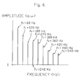
- the synchronous saw-tooth drive voltages include harmonic frequency components in addition to their fundamental frequency. Therefore, even when the fundamental frequency of the synchronous saw-tooth drive voltages is smaller than the natural frequencies of a mechanically-vibrating system of the mirror with respect to the Y-axis depending upon the structure of the outer piezoelectric actuators, one of the above-mentioned harmonic frequency components would coincide with one of the natural frequencies or be brought close to one of the natural frequencies.
- this harmonic frequency component of the drive voltages would resonate with such a natural frequency of the mechanically-vibrating system of the mirror with respect to the Y-axis, so that a higher frequency vibration would be superimposed onto the rocking of the mirror with respect to the Y-axis.
- one approach is to make the natural frequencies much larger than the fundamental frequency of the synchronous saw-tooth drive voltages. In this case, however, since the mechanically-vibrating system of the mirror including the outer piezoelectric actuators is hardened, it would be difficult to rock the mirror at a larger deflection angle.
- Another approach is to use synchronous sinusoidal-wave drive voltages whose frequency is much larger than the natural frequencies of the mechanically-vibrating system of the mirror with respect to the Y-axis, instead of the synchronous saw-tooth drive voltages.
- a linearly-deflected period within one period of the synchronous sinusoidal-wave drive voltages where the deflection angle is linearly changed becomes too small, i.e., an effective scanning period becomes too small, so it is not practical in an image display apparatus such as a projector to use such an optical deflector.
- the presently disclosed subject matter seeks to solve one or more of the above-described problems.
- an optical deflector comprising a mirror, a movable frame for supporting the mirror, a support body surrounding the movable frame, and a first group of piezoelectric actuators serving as cantilevers and a second group of piezoelectric actuators serving as cantilevers alternating with the first group of piezoelectric actuators
- the piezoelectric actuators are folded at every actuator and connected from the support body to the movable frame.
- Each of the piezoelectric actuators is in parallel with one axis of the mirror.
- a driver combines first and second original saw-tooth waves having the same waveform into first saw-tooth waves.
- the driver generates a first drive voltage having the first saw-tooth waves and applies the first drive voltage to the first group of piezoelectric actuators.
- the driver generates a second drive voltage having second saw-tooth waves opposite in phase to the first saw-tooth waves, and applies the second drive voltage to the second group of piezoelectric actuators.
- a difference in phase between the first and second original saw-tooth waves is a predetermined value to suppress the coincidence between a natural frequency of a mechanically-vibrating system of the mirror with respect to the axis thereof depending upon the piezoelectric actuators and the frequency of the mirror.
- the deflection angle can be linearly changed for a longer period, so that the optical deflector according to the presently disclosed subject matter can be applied to an image display apparatus such as a projector. Also, the resonance of the harmonic frequency components of the first and second drive voltages with the natural frequency components of the mechanically-vibrating system of the mirror can be suppressed.
- a method for setting drive data for driving an optical deflector including a mirror, a movable frame for supporting the mirror, a support body surrounding the movable frame, and a first group of piezoelectric actuators serving as cantilevers and a second group of piezoelectric actuators serving as cantilevers alternating with the first group of piezoelectric actuators, the piezoelectric actuators being folded at every actuator and connected from the support body to the movable frame, each of the piezoelectric actuators being in parallel with one axis of the mirror, a period is set common to first and second drive voltages for the first and second groups of piezoelectric actuators, respectively. Then, a ratio of a rising period to a falling period is designated.
- a total of the rising period and the falling period is equal to the period to select first original drive data forming a first original saw-tooth wave having the rising period and the falling period.
- the first original drive data is shifted by a shift value corresponding to a half wave-length of a natural frequency of a mechanically-vibrating system of the mirror with respect to the axis thereof depending upon the piezoelectric actuators to obtain second original drive data.
- the first and second original drive data are combined into first drive data forming a first saw-tooth wave for the first group of piezoelectric actuators.
- the first drive data is inverted to obtain second drive data forming a second saw-tooth wave for the second group of piezoelectric actuators.
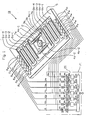
- Fig. 1 which illustrates an embodiment of the driver for driving an optical deflector according to the presently disclosed subject matter, an optical deflector 10 and its driver 20 are provided.
- the optical deflector 10 is constructed by a circular mirror 1 for reflecting an incident light, a movable frame 2 surrounding the mirror 1 for supporting the mirror 1 through a pair of torsion bars 3a and 3b, inner piezoelectric actuators 4a-1, 4a-2, 4b-1 and 4b-2 fixed between the movable frame 2 and the torsion bars 3a and 3b and serving as cantilevers for rocking the mirror 1 through the torsion bars 3a and 3b with respect to an X-axis of the mirror 1, a support body 5 surrounding the movable frame 2, outer piezoelectric actuators 6a-1, 6a-2, 6a-3 and 6a-4 and 6b-1, 6b-2, 6b-3 and 6b-4 fixed between the support body 5 and the movable frame 2 and serving as cantilevers for rocking the mirror 1 through the movable frame 2 with respect to a Y-axis of the mirror 1 perpendicular to the X-axis, and piezoelectric sensors 7a and 7b on the movable frame 2.
- the torsion bars 3a and 3b are arranged along the X-axis, and have ends coupled to the inner circumference of the movable frame 2 and other ends coupled to the outer circumference of the mirror 1. Therefore, the torsion bars 3a and 3b are twisted by the inner piezoelectric actuators 4a-1, 4a-2, 4b-1 and 4b-2 to rock the mirror 1 with respect to the X-axis.
- the inner piezoelectric actuators 4a-1 and 4b-1 oppose each other along the Y-axis and sandwich the torsion bar 3a.
- the inner piezoelectric actuators 4a-1 and 4b-1 have ends coupled to the inner circumference of the movable frame 2 and other ends coupled to the torsion bar 2a. In this case, the flexing direction of the inner piezoelectric actuator 4a-1 is opposite to that of the inner piezoelectric actuator 4b-1.
- the inner piezoelectric actuators 4a-2 and 4b-2 oppose each other along the Y-axis and sandwich the torsion bars 3b.
- the inner piezoelectric actuators 4a-2 and 4b-2 have ends coupled to the inner circumference of the movable frame 2 and other ends coupled to the torsion bar 2b. In this case, the flexing direction of the inner piezoelectric actuator 4a-2 is opposite to that of the inner piezoelectric actuator 4b-2.
- the support body 5 is rectangularly-framed to surround the movable frame 2.
- the outer piezoelectric actuators 6a-1, 6a-2, 6a-3 and 6a-4, 6b-1, 6b-2, 6b-3 and 6b-4 are coupled between the inner circumference of the support body 5 and the outer circumference of the movable frame 2, in order to rock the movable frame 2 associated with the mirror 1 with respect to the support body 5, i.e., to rock the mirror 1 with respect to the Y-axis.
- the outer piezoelectric actuators 6a-1, 6a-2, 6a-3 and 6a-4 are serially-coupled from the movable frame 2 to the support body 5. Also, each of the outer piezoelectric actuators 6a-1, 6a-2, 6a-3 and 6a-4 are in parallel with the X-axis of the mirror 1. Therefore, the outer piezoelectric actuators 6a-1, 6a-2, 6a-3 and 6a-4 are folded at every actuator or meandering from the support body 5 to the movable frame 2, so that the amplitudes of the outer piezoelectric actuators 6a-1, 6a-2, 6a-3 and 6a-4 can be changed along directions perpendicular to the Y-axis of the mirror 1.
- the outer piezoelectric actuators 6b-1, 6b-2, 6b-3 and 6b-4 are serially-coupled from the movable frame 2 to the support body 5. Also, each of the outer piezoelectric actuators 6b-1, 6b-2, 6b-3 and 6b-4 are in parallel with the X-axis of the mirror 1. Therefore, the outer piezoelectric actuators 6b-1, 6b-2, 6b-3 and 6b-4 are folded at every actuator or jetting from the support body 5 to the movable frame 2, so that the amplitudes of the outer piezoelectric actuators 6b-1, 6b-2, 6b-3 and 6b-4 can be changed along directions perpendicular to the Y-axis of the mirror 1.
- the piezoelectric sensors 7a and 7b sense a deflection angle A of the mirror 1 with respect to the Y-axis.
- pads P a1 , P a2 , P a3 , P a4 , P a5 and P a6 , P b1 , P b2 , P b3 ) P b4 , P b5 and P b6 which are connected to the driver 20.
- the pad P a1 is connected to the upper electrode layer 207 (see: Fig. 2 ) of each of the inner piezoelectric actuators 4a-1 and 4a-2, and the pad P a2 is connected to the lower electrode layer 205 (see: Fig. 2 ) of each of the inner piezoelectric actuators 4a-1 and 4a-2. Also, the pad P a3 is connected to the upper electrode layer 207 (see: Fig. 2 ) of each of the outer piezoelectric actuators 6a-1 and 6a-3, and the pad P a4 is connected to the upper electrode layer 207 (see: Fig. 2 ) of each of the outer piezoelectric actuators 6a-2 and 6a-4.
- the pad P a5 is connected to the lower electrode layer 205 (see: Fig. 2 ) of each of the outer piezoelectric actuators 6a-1, 6a-2, 6a-3 and 6a-4. Still further, the pad P a6 is connected to the upper electrode layer 207 (see: Fig. 2 ) of the piezoelectric sensor 7a.
- the pad P b1 is connected to the upper electrode layer 207 (see: Fig. 2 ) of each of the inner piezoelectric actuators 4b-1 and 4b-2
- the pad P b2 is connected to the lower electrode layer 205 (see: Fig. 2 ) of each of the inner piezoelectric actuators 4b-1 and 4b-2
- the pad P b3 is connected to the upper electrode layer 207 (see: Fig. 2 ) of each of the outer piezoelectric actuators 6b-1 and 6b-3
- the pad P b4 is connected to the upper electrode layer 207 (see: Fig. 2 ) of each of the outer piezoelectric actuators 6b-2 and 6b-4.
- the pad P b5 is connected to the lower electrode layer 205 (see: Fig. 2 ) of each of the outer piezoelectric actuators 6b-1, 6b-2, 6b-3 and 6b-4. Still further, the pad P b6 is connected to the upper electrode layer 207 of the piezoelectric sensor 7b.
- the driver 20 is constructed by a control circuit 21 such as a microcomputer including a central processing unit (CPU), a read-only memory (ROM), a random access memory (RAM), an input/output (I/O) interface and the like.
- a control circuit 21 such as a microcomputer including a central processing unit (CPU), a read-only memory (ROM), a random access memory (RAM), an input/output (I/O) interface and the like.
- the driver 20 further includes a nonvolatile memory 221 for storing drive data Xa for driving the upper electrode layers of the inner piezoelectric actuators 4a-1 and 4a-2, a digital-to-analog converter (DAC) 231 for converting the drive data Xa into a drive voltage V Xa , and a drive circuit 241 for applying the drive voltage V Xa to the pad P a1 .
- DAC digital-to-analog converter
- the driver 20 further includes a nonvolatile memory 222 for storing drive data Xb for driving the upper electrode layers of the inner piezoelectric actuators 4b-1 and 4b-2, a digital-to-analog converter (DAC) 232 for converting the drive data Xb into a drive voltage V Xb , and a drive circuit 242 for applying the drive voltage V Xb to the pad P b1 .
- DAC digital-to-analog converter
- the driver 20 further includes a nonvolatile memory 223 for storing reference data Xr for driving the lower electrode layers of the inner piezoelectric actuators 4a-1, 4a-2, 4b-1 and 4b-2, a digital-to-analog converter (DAC) 233 for converting the reference data Xr into a reference voltage V Xr , and a drive circuit 243 for applying the reference voltage V Xr to the pads P a2 and P b2 .
- DAC digital-to-analog converter
- the driver 20 further includes a nonvolatile memory 224 for storing drive data Y1 for driving the upper electrode layers of the outer piezoelectric actuators 6a-1, 6a-3, 6b-1 and 6b-3, a digital-to-analog converter (DAC) 234 for converting the drive data Y1 into a drive voltage V Y1 , and a drive circuit 244 for applying the drive voltage V Y1 to the pads P a3 and P b3 .
- DAC digital-to-analog converter
- the driver 20 further includes a nonvolatile memory 225 for storing drive data Y2 for driving the upper electrode layers of the outer piezoelectric actuators 6a-2, 6a-4, 6b-2 and 6b-4, a digital-to-analog converter (DAC) 235 for converting the drive data Y2 into a drive voltage V Y2 , and a drive circuit 245 for applying the drive voltage V Y2 to the pads P a4 and P b4 .
- DAC digital-to-analog converter
- the driver 20 further includes a nonvolatile memory 226 for storing reference data Yr for driving the lower electrode layers of the outer piezoelectric actuators 6a-1, 6a-2, 6a-3, 6a-4, 6b-1, 6b-2, 6b-3 and 6b-4, a digital-to-analog converter (DAC) 236 for converting the reference data Yr into a reference voltage V Yr , and a drive circuit 246 for applying the reference voltage V Yr to the pads P a5 and P b5 .
- DAC digital-to-analog converter
- the driver 20 further includes an amplifier 251 for amplifying an analog deflection angle A of the mirror 1 from the pads P a6 and P b6 and an analog-to-digital converter (ADC) 252 for converting the analog deflection angle A into a digital deflection angle data.
- ADC analog-to-digital converter
- the number of the outer piezoelectric actuators 6a-1, 6a-2, 6a-3 and 6a-4 and the number of the outer piezoelectric actuators 6b-1, 6b-2, 6b-3 and 6b-4 can be other values such as 2, 6, 8, ⁇ .
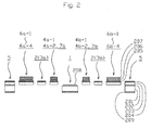
- a monocrystalline silicon support layer 201, an intermediate silicon oxide layer 202 and a monocrystalline silicon active layer 203 are formed by a silicon-on-insulator (SOI) substrate.
- reference numeral 204 designates a silicon oxide layer
- 205 designates a lower electrode layer made of Pt, Au or the like
- 206 designates a lead titanate zirconate (PZT) layer
- 207 designates an upper electrode layer made of Pt, Au or the like
- 208 designates a metal layer made of Al, Ag or the like
- 209 designates a hard mask layer made of silicon oxide or the like.
- the mirror 1 is constructed by the monocrystalline silicon support layer 201 serving as a vibration plate, the metal layer 208 serving as a reflector and the hard mask layer 209.
- the movable frame 2 as well as the torsion bars 3a and 3b are constructed by the monocrystalline silicon active layer 203 and the silicon oxide layer 204.
- the inner piezoelectric actuators 4a-1, 4a-2, 4b-1 and 4b-2 and the outer piezoelectric actuators 6a-1 to 6a-4 and 6b-1 to 6b-4 and the piezoelectric sensors 7a and 7b are constructed by the monocrystalline silicon active layer 203, the silicon oxide layer 204, the lower electrode layer 205, the PZT layer 206 and the upper electrode layer 207.
- the support body 5 is constructed by the monocrystalline silicon layer 201, the intermediate silicon layer 202, the monocrystalline silicon active layer 203, the silicon oxide layer 204 and the hard mask layer 209.
- the pads P a1 , P a2 , P a3 , P a4 , P a5 and P a6 , P b1 , P b2 , P b3 ) P b4 , P b5 and P b6 are constructed by the lower electrode layer 205.
- the drive voltage V Xa based upon the drive data Xa stored in advance in the nonvolatile memory 221 and the drive voltage V Xb based upon the drive data Xb stored in advance in the nonvolatile memory 222 are sinusoidal at a predetermined frequency such as 15 kHz and symmetrical or opposite in phase to each other with the reference voltage V Xr based upon the reference data Xr stored in advance in the nonvolatile memory 223.
- the inner piezoelectric actuators 4a-1 and 4a-2 and the inner piezoelectric actuators 4b-1 and 4b-2 carry out flexing operations in opposite directions to each other, so that the torsion bars 3a and 3b are twisted to rock the mirror 1 with respect to the X-axis.
- the rising and falling timings of the drive voltage V Xa coincide with the falling and rising timings, respectively, of the drive voltage V Xb , so the drive voltages V Xa and V Xb can be said to be synchronous with each other.
- the outer piezoelectric actuators 6a-1, 6a-2, 6a-3, 6a-4, 6b-1, 6b-2, 6b-3 and 6b-4 are divided into an odd-numbered group of the outer piezoelectric actuators 6a-1 and 6a-3; 6b-1 and 6b-3, and an even-numbered group of the outer piezoelectric actuators 6a-2 and 6a-4; 6b-2 and 6b-4 alternating with the odd-numbered group of the outer piezoelectric actuators 6a-1 and 6a-3; 6b-1 and 6b-3.
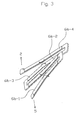
- Fig. 3 which illustrates only the outer piezoelectric actuators 6b-1, 6b-2, 6b-3 and 6b-4
- the odd-numbered group of the outer piezoelectric actuators 6a-1, 6a-3, 6b-1 and 6b-3 are flexed in one direction, for example, in a downward direction
- the even-numbered group of the outer piezoelectric actuators 6a-2, 6a-4, 6b-2 and 6b-4 are flexed in the other direction, i. e. , in an upward direction.
- the even-numbered group of the outer piezoelectric actuators 6a-2, 6a-4, 6b-2 and 6b-4 are flexed in the downward direction.
- the mirror 1 is rocked with respect to the Y-axis.
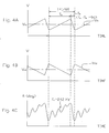
- modified synchronous saw-tooth drive voltages V Y1 and V Y2 are used instead of the synchronous saw-tooth drive voltages V Y1 and V Y2 of Figs. 4A and 4B , so that the high harmonic components caused by the resonance of the drive voltages V Y1 and V Y2 with the natural frequency f c can be compensated for. Also, the amplitudes of the drive voltages V Y1 and V Y2 are adjusted, so that the above-mentioned high harmonic components can be more completely compensated for.
- Fig. 7 is a flowchart for explaining an example of setting the drive data V Y1 and V Y2 of the outer piezoelectric actuators as an operation of the control circuit 21 of Fig. 1 .
- a period T of the drive voltages V Y1 and V Y2 is set in accordance with the customer's request and so on. For example, if the vertical deflection is carried out at a frequency of 60 Hz, T ⁇ 1 / 60 where T is a period.
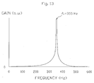
- the CPU of the control circuit 21 calculates a natural frequency f c of the mechanically-vibrating system of the mirror 1 with respect to the Y-axis depending upon the structure of the outer piezoelectric actuators 6a-1, 6a-2, 6a-3 and 6a-4, 6b-1, 6b-2, 6b-3 and 6b-4.
- E is a modulus of direct elasticity of the piezoelectric actuators 6a-1, 6a-2, 6a-3 and 6a-4, 6b-1, 6b-2, 6b-3 and 6b-4;
- t is a thickness of the piezoelectric actuators 6a-1, 6a-2, 6a-3 and 6a-4, 6b-1, 6b-2, 6b-3 and 6b-4;
- ⁇ is
- a first original saw-tooth drive data Y11 is selected by designating a ratio of T 0a to T 0b .
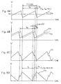
- the saw-tooth drive voltage V Y1 for the first original saw-tooth drive data Y11 as illustrated in Fig. 8A is selected.
- the first original drive data Y11 is shifted by a half phase ⁇ ⁇ of the resonance frequency (natural frequency) f c to obtain second original drive data Y12 as illustrated in Fig. 8B .
- step 705 the first and second original saw-tooth drive data Y11 and Y12 are combined into saw-tooth drive data Y1 for a drive voltage V Y1 as illustrated in Fig. 8C .
- Y ⁇ 1 t ⁇ ⁇ Y ⁇ 11 t + Y ⁇ 12 t + ⁇
- t is a time
- ⁇ is a positive value such as 1/2
- ⁇ is an offset value.
- the offset value ⁇ is determined in such a way that the minimum value of the saw-tooth drive data Y1 is zero.
- the saw-tooth drive data Y1 has the frequency f 0 , i.e., the period T and the definite amplitude.
- T a T 0 ⁇ a - ⁇ ⁇ ⁇ / 360 ⁇ 1 / f 0
- T b T 0 ⁇ b + ⁇ ⁇ ⁇ / 360 ⁇ 1 / f 0
- T a > T b T a • T 0 ⁇ a > 1 / 2 + ⁇ ⁇ ⁇ / 360 or f 0 • T 0 ⁇ b ⁇ 1 / 2 + ⁇ ⁇ ⁇ / 360
- the drive data Y1 is inverted with respect to the reference data Yr into drive data Y2. That is, the drive voltage V Y1 as illustrated in Fig. 8C is inverted with respect to the reference voltage V Yr into a T b :T a saw-tooth drive voltage V Y2 , as illustrated in Fig. 8D .
- step 707 the amplitudes of the drive voltages V Y1 and V Y2 , i. e. , the drive data Y1 and Y2 are adjusted for the reason that will be discussed later.
- step 708 the drive data Y1 for the drive voltage V Y1 and the drive data Y2 for the drive voltage V Y2 are stored in the nonvolatile memories 224 and 225, respectively.
- step 709 the routine of Fig. 7 is completed by step 709.
- steps 703, 704, 705 and 706 the two synchronous drive data Y1 and Y2 for the synchronous drive voltages V Y1 and V Y2 are obtained.
- a deflection angle A1 of the mirror 1 indicated by a solid line in Fig. 9 would be obtained.
- the natural frequency f c included in the deflection angle A1 and the high frequency component, i.e., the natural frequency f c included in the deflection angle A2 are compensated for by each other.
- the amplitude of the high frequency component f c included in the deflection angle A1 is different from the amplitude of the high frequency component f c included in the deflection angle A2 due to the length of connections and the loads of the outer piezoelectric actuators 6a-1, 6a-2, 6a-3 and 6a-4; 6b-1, 6b-2, 6b-3 and 6b-4 and so on.
- the amplitude of the drive voltage V Y1 and/or the amplitude of the drive voltage V Y2 i.e., the drive data Y1 and/or Y2 are adjusted in such a way that the amplitude of the deflection angle A1 when only the drive voltage V Y1 is applied without applying the drive voltage V Y2 is equal to the amplitude of the deflection angle A2 when only the drive voltage V Y2 is applied without applying the drive voltage V Y1 .
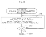
- Fig. 10 is a flowchart for explaining the driving of the outer piezoelectric actuators as an operation of the control circuit 21 of Fig. 1 in accordance with the drive data Y1, Y2 and Yr stored in the nonvolatile memories 224, 225 and 226 by the routine of Fig. 7 .
- the drive data Y1 and Y2 are sequentially read out of the nonvolatile memories 224 and 225, so that the drive voltage V Y1 as illustrated in Fig. 8C is applied to the odd-numbered group of the outer piezoelectric actuators 6a-1, 6a-3, 6b-1 and 6b-3, and the drive voltage V Y2 as illustrated in Fig. 8D is applied to the even-numbered group of the outer piezoelectric actuators 6a-2, 6a-4, 6b-2 and 6b-4.
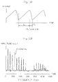
- a deflection angle A of the mirror 1 as illustrated in Fig. 11A is read from the pads P a6 and P b6 .
- the deflection angle A includes no resonance frequency component f c .
- step 1001 of Fig. 10 is repeated by step 1002 until a stop message is input or generated.
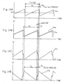
- modified synchronous saw-tooth drive voltages V Y1 and V Y2 generated by the flowchart of Fig. 7 are used instead of the synchronous saw-tooth drive voltages V Y1 and V Y2 of Figs. 12A and 12B , so that the high harmonic components caused by the resonance of the drive voltages V Y1 and V Y2 with the natural frequency f c can be compensated for. Also, the amplitudes of the drive voltages V Y1 and V Y2 are adjusted, so that the above-mentioned high harmonic components can be more completely compensated for.
- a first original saw-tooth drive data Y11 is selected by designating a ratio of T 0a to T0 b .
- the saw-tooth drive voltage V Y1 for the first original saw-tooth drive data Y11 as illustrated in Fig. 14A is selected.
- the first and second original saw-tooth drive data Y11 and Y12 are combined into saw-tooth drive data Y1 for a drive voltage V Y1 as illustrated in Fig. 14C .
- the drive data Y1 is inverted with respect to the reference data Yr into drive data Y2. That is, the drive voltage V Y1 as illustrated in Fig. 14C is inverted with respect to the reference voltage V Y1 into a T b :T a saw-tooth drive voltage V Y2 , as illustrated in Fig. 14D .
- step 1001 note that the drive voltage V Y1 as illustrated in Fig. 8C can be applied to the even-numbered group of the outer piezoelectric actuators 6a-2, 6a-4, 6b-2 and 6b-4, and the drive voltage V Y2 as illustrated in Fig. 8D can be applied to the odd-numbered group of the outer piezoelectric actuators 6a-1, 6a-3, 6b-1 and 6b-3.
- the deflection angle can be linearly changed for a longer period so that the optical deflector according to the presently disclosed subject matter can be applied to an image display apparatus such as a projector.
- the resonation of the harmonic frequency components of the drive voltage V Y1 and V Y2 with the natural frequency components of the mechanically-vibrating system of the mirror 1 can be suppressed.
- routines of Figs. 7 and 10 are stored as programs in the ROM or the like of the control circuit 21.
- the two-dimensional optical deflector of Fig. 1 has the same inner piezoelectric actuators without the torsion bars as the outer piezoelectric actuators, the presently disclosed subject matter can also be applied to such an optical deflector.
- the presently disclosed subject matter can be applied to a one-dimensional optical deflector which is constructed by a mirror; a movable frame for supporting the mirror; a support body surrounding the movable frame; and piezoelectric actuators fixed between the support body and the movable frame and serving as cantilevers for rocking the mirror through the movable frame with respect to an axis of the mirror.
- the movable frame may be a movable frame.
Landscapes
- Physics & Mathematics (AREA)
- General Physics & Mathematics (AREA)
- Optics & Photonics (AREA)
- Mechanical Optical Scanning Systems (AREA)
- Mechanical Light Control Or Optical Switches (AREA)
- General Electrical Machinery Utilizing Piezoelectricity, Electrostriction Or Magnetostriction (AREA)
- Micromachines (AREA)
Applications Claiming Priority (1)
| Application Number | Priority Date | Filing Date | Title |
|---|---|---|---|
| JP2011062919A JP5659056B2 (ja) | 2011-03-22 | 2011-03-22 | 光偏向器の駆動装置 |
Publications (3)
| Publication Number | Publication Date |
|---|---|
| EP2503375A2 true EP2503375A2 (de) | 2012-09-26 |
| EP2503375A3 EP2503375A3 (de) | 2017-06-14 |
| EP2503375B1 EP2503375B1 (de) | 2020-02-26 |
Family
ID=45999518
Family Applications (1)
| Application Number | Title | Priority Date | Filing Date |
|---|---|---|---|
| EP12001941.9A Active EP2503375B1 (de) | 2011-03-22 | 2012-03-20 | Treiber für optischen Deflektor unter Verwendung zweier veränderter asynchroner Sägezahn-Treiberspannungen und Verfahren zu dessen Einstellung |
Country Status (4)
| Country | Link |
|---|---|
| US (1) | US8841821B2 (de) |
| EP (1) | EP2503375B1 (de) |
| JP (1) | JP5659056B2 (de) |
| CN (1) | CN102692704B (de) |
Cited By (2)
| Publication number | Priority date | Publication date | Assignee | Title |
|---|---|---|---|---|
| EP2818909A4 (de) * | 2012-02-22 | 2015-11-11 | Funai Electric Co | Bildanzeigevorrichtung und spiegelantriebsverfahren dafür |
| EP3109685A1 (de) * | 2015-06-22 | 2016-12-28 | Ricoh Company, Ltd. | Optische deflektorvorrichtung, bilderzeugungsvorrichtung, bildanzeigevorrichtung, objektvorrichtung und einstellungsverfahren einer optischen deflektorvorrichtung |
Families Citing this family (29)
| Publication number | Priority date | Publication date | Assignee | Title |
|---|---|---|---|---|
| US8593764B1 (en) * | 2011-06-14 | 2013-11-26 | Western Digital Technologies, Inc. | Method for fine actuation of a head during operation of a disk drive |
| US8446694B1 (en) | 2011-06-14 | 2013-05-21 | Western Digital Technologies, Inc. | Disk drive head suspension assembly with embedded in-plane actuator at flexure tongue |
| US9287488B2 (en) * | 2012-01-31 | 2016-03-15 | Panasonic Intellectual Property Management Co., Ltd. | Piezoelectric actuator device and method for manufacturing same |
| JP2014087169A (ja) * | 2012-10-24 | 2014-05-12 | Seiko Epson Corp | 駆動装置、駆動回路、ロボットハンド、ロボット、電子部品搬送装置、電子部品検査装置、送液ポンプ、印刷装置、電子時計、投影装置 |
| JP6092589B2 (ja) * | 2012-11-19 | 2017-03-08 | スタンレー電気株式会社 | 光偏向器 |
| JP2014102355A (ja) * | 2012-11-19 | 2014-06-05 | Stanley Electric Co Ltd | 光偏向器 |
| JP2014130257A (ja) * | 2012-12-28 | 2014-07-10 | Jvc Kenwood Corp | 画像表示装置、画像表示方法及びプログラム |
| US8982513B1 (en) | 2013-05-21 | 2015-03-17 | Western Digital Technologies, Inc. | Disk drive head suspension with dual piezoelectric elements adhered to rotary-actuated and non-actuated portions of a structural layer of a tongue of a laminated flexure |
| JP6149516B2 (ja) * | 2013-06-03 | 2017-06-21 | ミツミ電機株式会社 | 光走査装置、光走査制御装置及び光走査ユニット |
| JP6189137B2 (ja) * | 2013-08-23 | 2017-08-30 | スタンレー電気株式会社 | 光スキャナ |
| JP6168353B2 (ja) | 2013-09-13 | 2017-07-26 | 株式会社リコー | 光偏向装置、画像形成装置、車両、光偏向装置の制御方法、及び光偏向装置の調整方法 |
| JP6311314B2 (ja) * | 2014-01-06 | 2018-04-18 | 株式会社リコー | 光偏向装置、光走査装置、画像表示装置及び画像形成装置 |
| JP6641709B2 (ja) * | 2014-07-03 | 2020-02-05 | 株式会社リコー | 光偏向装置、画像形成装置、画像表示装置、移動体装置、及び光偏向装置の調整方法 |
| JP2016148763A (ja) * | 2015-02-12 | 2016-08-18 | スタンレー電気株式会社 | 映像投射装置 |
| JP6891402B2 (ja) * | 2015-06-22 | 2021-06-18 | 株式会社リコー | 光偏向装置、画像形成装置、画像表示装置、物体装置、及び光偏向装置の調整方法 |
| JP6808506B2 (ja) * | 2017-01-25 | 2021-01-06 | スタンレー電気株式会社 | 光走査装置 |
| JP7011164B2 (ja) * | 2018-03-15 | 2022-02-10 | ミツミ電機株式会社 | アクチュエータ及び光走査装置 |
| JP7011165B2 (ja) * | 2018-03-22 | 2022-01-26 | ミツミ電機株式会社 | アクチュエータ及び光走査装置 |
| JP7021435B2 (ja) | 2018-04-18 | 2022-02-17 | ミツミ電機株式会社 | ミラー駆動装置、光走査制御装置及びミラー駆動方法 |
| JP7161094B2 (ja) * | 2018-04-18 | 2022-10-26 | ミツミ電機株式会社 | 走査駆動装置、光走査制御装置及び駆動波形生成方法 |
| CN110764251B (zh) * | 2018-07-25 | 2021-11-09 | 中国科学院苏州纳米技术与纳米仿生研究所 | 驱动扫描微镜进行转动的方法及其装置 |
| JP7157332B2 (ja) * | 2018-12-28 | 2022-10-20 | ミツミ電機株式会社 | 光走査装置及びその制御方法 |
| JP7177351B2 (ja) | 2019-02-25 | 2022-11-24 | ミツミ電機株式会社 | 光走査装置及びその制御方法 |
| JP7263918B2 (ja) * | 2019-05-21 | 2023-04-25 | 株式会社リコー | 光偏向装置、画像投影装置、車両、及び調整方法 |
| JP7315827B2 (ja) | 2019-07-01 | 2023-07-27 | ミツミ電機株式会社 | 光走査装置及びその制御方法 |
| CN112782845B (zh) * | 2020-12-31 | 2023-02-21 | 歌尔股份有限公司 | Mems扫描镜及激光投影仪 |
| CN112817141B (zh) * | 2020-12-31 | 2023-03-24 | 歌尔股份有限公司 | Mems扫描镜及其驱动方法、激光投影仪 |
| JP2022185637A (ja) * | 2021-06-03 | 2022-12-15 | スタンレー電気株式会社 | 光偏向器 |
| EP4715445A1 (de) | 2024-03-01 | 2026-03-25 | Yitoa Aurora Micro Technology Corporation | Antriebsvorrichtung für einen beweglichen körper und vorrichtung zur ablenkung eines beweglichen körpers |
Citations (2)
| Publication number | Priority date | Publication date | Assignee | Title |
|---|---|---|---|---|
| JP2009223165A (ja) | 2008-03-18 | 2009-10-01 | Stanley Electric Co Ltd | 光偏向器 |
| JP2011062919A (ja) | 2009-09-17 | 2011-03-31 | Sekisui Chem Co Ltd | 多層離型フィルム |
Family Cites Families (8)
| Publication number | Priority date | Publication date | Assignee | Title |
|---|---|---|---|---|
| JP4881073B2 (ja) * | 2006-05-30 | 2012-02-22 | キヤノン株式会社 | 光偏向器、及びそれを用いた光学機器 |
| JP2007322466A (ja) * | 2006-05-30 | 2007-12-13 | Canon Inc | 光偏向器、及びそれを用いた光学機器 |
| CN101598852A (zh) * | 2006-06-07 | 2009-12-09 | 佳能株式会社 | 振荡器装置、光偏转器以及使用光偏转器的光学器械 |
| JP2009223115A (ja) * | 2008-03-18 | 2009-10-01 | Panasonic Corp | 光学反射素子 |
| JP5446122B2 (ja) * | 2008-04-25 | 2014-03-19 | パナソニック株式会社 | ミアンダ形振動子およびこれを用いた光学反射素子 |
| JP5181892B2 (ja) * | 2008-07-16 | 2013-04-10 | ブラザー工業株式会社 | 駆動信号発生器及びそれを備えた光走査装置並びに画像表示装置 |
| JP5493735B2 (ja) * | 2009-01-30 | 2014-05-14 | 株式会社リコー | 偏向ミラー、光走査装置、画像形成装置、および画像投影装置 |
| JP5152075B2 (ja) * | 2009-03-31 | 2013-02-27 | ブラザー工業株式会社 | 駆動信号発生器及びそれを備えた光走査装置並びに画像表示装置 |
-
2011
- 2011-03-22 JP JP2011062919A patent/JP5659056B2/ja active Active
-
2012
- 2012-03-20 EP EP12001941.9A patent/EP2503375B1/de active Active
- 2012-03-21 US US13/426,276 patent/US8841821B2/en active Active
- 2012-03-22 CN CN201210077887.5A patent/CN102692704B/zh active Active
Patent Citations (2)
| Publication number | Priority date | Publication date | Assignee | Title |
|---|---|---|---|---|
| JP2009223165A (ja) | 2008-03-18 | 2009-10-01 | Stanley Electric Co Ltd | 光偏向器 |
| JP2011062919A (ja) | 2009-09-17 | 2011-03-31 | Sekisui Chem Co Ltd | 多層離型フィルム |
Cited By (2)
| Publication number | Priority date | Publication date | Assignee | Title |
|---|---|---|---|---|
| EP2818909A4 (de) * | 2012-02-22 | 2015-11-11 | Funai Electric Co | Bildanzeigevorrichtung und spiegelantriebsverfahren dafür |
| EP3109685A1 (de) * | 2015-06-22 | 2016-12-28 | Ricoh Company, Ltd. | Optische deflektorvorrichtung, bilderzeugungsvorrichtung, bildanzeigevorrichtung, objektvorrichtung und einstellungsverfahren einer optischen deflektorvorrichtung |
Also Published As
| Publication number | Publication date |
|---|---|
| US8841821B2 (en) | 2014-09-23 |
| EP2503375B1 (de) | 2020-02-26 |
| JP5659056B2 (ja) | 2015-01-28 |
| JP2012198415A (ja) | 2012-10-18 |
| US20120242191A1 (en) | 2012-09-27 |
| CN102692704B (zh) | 2016-02-10 |
| CN102692704A (zh) | 2012-09-26 |
| EP2503375A3 (de) | 2017-06-14 |
Similar Documents
| Publication | Publication Date | Title |
|---|---|---|
| EP2503375B1 (de) | Treiber für optischen Deflektor unter Verwendung zweier veränderter asynchroner Sägezahn-Treiberspannungen und Verfahren zu dessen Einstellung | |
| EP2495601A1 (de) | Treiber für optischen Deflektor unter Verwendung zwei asynchroner Sägezahn-Treiberspannungen und Verfahren zu dessen Einstellung | |
| US8649078B2 (en) | Driver for optical deflector using complex-sinusoidal-wave drive voltages and method for setting the same | |
| US8922861B2 (en) | Two-dimensional optical deflector apparatus using curved-type saw-tooth drive voltages | |
| JP6333079B2 (ja) | 光スキャナ | |
| JP6220561B2 (ja) | 光偏向器 | |
| JP5157857B2 (ja) | 振動ミラー素子 | |
| JP2013205818A (ja) | 光偏向器 | |
| JP5967145B2 (ja) | 光走査装置 | |
| US8649080B2 (en) | Two-dimensional optical deflector including only one pair of meander-type piezoelectric actuators and its driver | |
| EP2953125A1 (de) | Treiber für optischen deflektor unter verwendung einer kombinierten sägezahn-treiberspannung und verfahren zur steuerung davon | |
| JP2014232176A (ja) | 光偏向器の製造方法及び光偏向器 | |
| JP2011069954A (ja) | 光スキャナ | |
| CN112817141B (zh) | Mems扫描镜及其驱动方法、激光投影仪 | |
| JP2014102355A (ja) | 光偏向器 | |
| JP5434541B2 (ja) | 2次元光走査装置 | |
| JP5299489B2 (ja) | アクチュエータ、光スキャナ、および画像形成装置 | |
| JP5299482B2 (ja) | アクチュエータ、光スキャナ、および画像形成装置 | |
| JP5344071B2 (ja) | アクチュエータ、光スキャナ、および画像形成装置 | |
| JP2014102354A (ja) | 光偏向器 | |
| JP5246367B2 (ja) | アクチュエータ、光スキャナ、および画像形成装置 | |
| JP2014164101A (ja) | 光偏向器 | |
| JP5664711B2 (ja) | アクチュエータ、光スキャナ、および画像形成装置 | |
| JP2013015834A (ja) | アクチュエータ、光スキャナ、および画像形成装置 |
Legal Events
| Date | Code | Title | Description |
|---|---|---|---|
| PUAI | Public reference made under article 153(3) epc to a published international application that has entered the european phase |
Free format text: ORIGINAL CODE: 0009012 |
|
| AK | Designated contracting states |
Kind code of ref document: A2 Designated state(s): AL AT BE BG CH CY CZ DE DK EE ES FI FR GB GR HR HU IE IS IT LI LT LU LV MC MK MT NL NO PL PT RO RS SE SI SK SM TR |
|
| AX | Request for extension of the european patent |
Extension state: BA ME |
|
| PUAL | Search report despatched |
Free format text: ORIGINAL CODE: 0009013 |
|
| AK | Designated contracting states |
Kind code of ref document: A3 Designated state(s): AL AT BE BG CH CY CZ DE DK EE ES FI FR GB GR HR HU IE IS IT LI LT LU LV MC MK MT NL NO PL PT RO RS SE SI SK SM TR |
|
| AX | Request for extension of the european patent |
Extension state: BA ME |
|
| RIC1 | Information provided on ipc code assigned before grant |
Ipc: G02B 26/08 20060101AFI20170509BHEP Ipc: H02N 2/00 20060101ALN20170509BHEP Ipc: G02B 26/10 20060101ALN20170509BHEP |
|
| STAA | Information on the status of an ep patent application or granted ep patent |
Free format text: STATUS: REQUEST FOR EXAMINATION WAS MADE |
|
| 17P | Request for examination filed |
Effective date: 20171214 |
|
| RBV | Designated contracting states (corrected) |
Designated state(s): AL AT BE BG CH CY CZ DE DK EE ES FI FR GB GR HR HU IE IS IT LI LT LU LV MC MK MT NL NO PL PT RO RS SE SI SK SM TR |
|
| GRAP | Despatch of communication of intention to grant a patent |
Free format text: ORIGINAL CODE: EPIDOSNIGR1 |
|
| STAA | Information on the status of an ep patent application or granted ep patent |
Free format text: STATUS: GRANT OF PATENT IS INTENDED |
|
| RIC1 | Information provided on ipc code assigned before grant |
Ipc: G02B 26/08 20060101AFI20190912BHEP Ipc: H02N 2/00 20060101ALN20190912BHEP Ipc: G02B 26/10 20060101ALN20190912BHEP |
|
| RIC1 | Information provided on ipc code assigned before grant |
Ipc: G02B 26/08 20060101AFI20190916BHEP Ipc: H02N 2/00 20060101ALN20190916BHEP Ipc: G02B 26/10 20060101ALN20190916BHEP |
|
| INTG | Intention to grant announced |
Effective date: 20191004 |
|
| RIN1 | Information on inventor provided before grant (corrected) |
Inventor name: AIMONO, TAKANORI |
|
| GRAS | Grant fee paid |
Free format text: ORIGINAL CODE: EPIDOSNIGR3 |
|
| GRAA | (expected) grant |
Free format text: ORIGINAL CODE: 0009210 |
|
| STAA | Information on the status of an ep patent application or granted ep patent |
Free format text: STATUS: THE PATENT HAS BEEN GRANTED |
|
| AK | Designated contracting states |
Kind code of ref document: B1 Designated state(s): AL AT BE BG CH CY CZ DE DK EE ES FI FR GB GR HR HU IE IS IT LI LT LU LV MC MK MT NL NO PL PT RO RS SE SI SK SM TR |
|
| REG | Reference to a national code |
Ref country code: GB Ref legal event code: FG4D |
|
| REG | Reference to a national code |
Ref country code: CH Ref legal event code: EP |
|
| REG | Reference to a national code |
Ref country code: DE Ref legal event code: R096 Ref document number: 602012068002 Country of ref document: DE |
|
| REG | Reference to a national code |
Ref country code: AT Ref legal event code: REF Ref document number: 1238354 Country of ref document: AT Kind code of ref document: T Effective date: 20200315 |
|
| REG | Reference to a national code |
Ref country code: IE Ref legal event code: FG4D |
|
| PG25 | Lapsed in a contracting state [announced via postgrant information from national office to epo] |
Ref country code: FI Free format text: LAPSE BECAUSE OF FAILURE TO SUBMIT A TRANSLATION OF THE DESCRIPTION OR TO PAY THE FEE WITHIN THE PRESCRIBED TIME-LIMIT Effective date: 20200226 Ref country code: NO Free format text: LAPSE BECAUSE OF FAILURE TO SUBMIT A TRANSLATION OF THE DESCRIPTION OR TO PAY THE FEE WITHIN THE PRESCRIBED TIME-LIMIT Effective date: 20200526 Ref country code: RS Free format text: LAPSE BECAUSE OF FAILURE TO SUBMIT A TRANSLATION OF THE DESCRIPTION OR TO PAY THE FEE WITHIN THE PRESCRIBED TIME-LIMIT Effective date: 20200226 |
|
| REG | Reference to a national code |
Ref country code: NL Ref legal event code: MP Effective date: 20200226 |
|
| REG | Reference to a national code |
Ref country code: LT Ref legal event code: MG4D |
|
| PG25 | Lapsed in a contracting state [announced via postgrant information from national office to epo] |
Ref country code: BG Free format text: LAPSE BECAUSE OF FAILURE TO SUBMIT A TRANSLATION OF THE DESCRIPTION OR TO PAY THE FEE WITHIN THE PRESCRIBED TIME-LIMIT Effective date: 20200526 Ref country code: GR Free format text: LAPSE BECAUSE OF FAILURE TO SUBMIT A TRANSLATION OF THE DESCRIPTION OR TO PAY THE FEE WITHIN THE PRESCRIBED TIME-LIMIT Effective date: 20200527 Ref country code: IS Free format text: LAPSE BECAUSE OF FAILURE TO SUBMIT A TRANSLATION OF THE DESCRIPTION OR TO PAY THE FEE WITHIN THE PRESCRIBED TIME-LIMIT Effective date: 20200626 Ref country code: LV Free format text: LAPSE BECAUSE OF FAILURE TO SUBMIT A TRANSLATION OF THE DESCRIPTION OR TO PAY THE FEE WITHIN THE PRESCRIBED TIME-LIMIT Effective date: 20200226 Ref country code: SE Free format text: LAPSE BECAUSE OF FAILURE TO SUBMIT A TRANSLATION OF THE DESCRIPTION OR TO PAY THE FEE WITHIN THE PRESCRIBED TIME-LIMIT Effective date: 20200226 Ref country code: HR Free format text: LAPSE BECAUSE OF FAILURE TO SUBMIT A TRANSLATION OF THE DESCRIPTION OR TO PAY THE FEE WITHIN THE PRESCRIBED TIME-LIMIT Effective date: 20200226 |
|
| PG25 | Lapsed in a contracting state [announced via postgrant information from national office to epo] |
Ref country code: NL Free format text: LAPSE BECAUSE OF FAILURE TO SUBMIT A TRANSLATION OF THE DESCRIPTION OR TO PAY THE FEE WITHIN THE PRESCRIBED TIME-LIMIT Effective date: 20200226 |
|
| PG25 | Lapsed in a contracting state [announced via postgrant information from national office to epo] |
Ref country code: ES Free format text: LAPSE BECAUSE OF FAILURE TO SUBMIT A TRANSLATION OF THE DESCRIPTION OR TO PAY THE FEE WITHIN THE PRESCRIBED TIME-LIMIT Effective date: 20200226 Ref country code: DK Free format text: LAPSE BECAUSE OF FAILURE TO SUBMIT A TRANSLATION OF THE DESCRIPTION OR TO PAY THE FEE WITHIN THE PRESCRIBED TIME-LIMIT Effective date: 20200226 Ref country code: SK Free format text: LAPSE BECAUSE OF FAILURE TO SUBMIT A TRANSLATION OF THE DESCRIPTION OR TO PAY THE FEE WITHIN THE PRESCRIBED TIME-LIMIT Effective date: 20200226 Ref country code: SM Free format text: LAPSE BECAUSE OF FAILURE TO SUBMIT A TRANSLATION OF THE DESCRIPTION OR TO PAY THE FEE WITHIN THE PRESCRIBED TIME-LIMIT Effective date: 20200226 Ref country code: EE Free format text: LAPSE BECAUSE OF FAILURE TO SUBMIT A TRANSLATION OF THE DESCRIPTION OR TO PAY THE FEE WITHIN THE PRESCRIBED TIME-LIMIT Effective date: 20200226 Ref country code: CZ Free format text: LAPSE BECAUSE OF FAILURE TO SUBMIT A TRANSLATION OF THE DESCRIPTION OR TO PAY THE FEE WITHIN THE PRESCRIBED TIME-LIMIT Effective date: 20200226 Ref country code: PT Free format text: LAPSE BECAUSE OF FAILURE TO SUBMIT A TRANSLATION OF THE DESCRIPTION OR TO PAY THE FEE WITHIN THE PRESCRIBED TIME-LIMIT Effective date: 20200719 Ref country code: RO Free format text: LAPSE BECAUSE OF FAILURE TO SUBMIT A TRANSLATION OF THE DESCRIPTION OR TO PAY THE FEE WITHIN THE PRESCRIBED TIME-LIMIT Effective date: 20200226 Ref country code: LT Free format text: LAPSE BECAUSE OF FAILURE TO SUBMIT A TRANSLATION OF THE DESCRIPTION OR TO PAY THE FEE WITHIN THE PRESCRIBED TIME-LIMIT Effective date: 20200226 |
|
| REG | Reference to a national code |
Ref country code: CH Ref legal event code: PL |
|
| REG | Reference to a national code |
Ref country code: AT Ref legal event code: MK05 Ref document number: 1238354 Country of ref document: AT Kind code of ref document: T Effective date: 20200226 |
|
| REG | Reference to a national code |
Ref country code: DE Ref legal event code: R097 Ref document number: 602012068002 Country of ref document: DE |
|
| PG25 | Lapsed in a contracting state [announced via postgrant information from national office to epo] |
Ref country code: MC Free format text: LAPSE BECAUSE OF FAILURE TO SUBMIT A TRANSLATION OF THE DESCRIPTION OR TO PAY THE FEE WITHIN THE PRESCRIBED TIME-LIMIT Effective date: 20200226 |
|
| REG | Reference to a national code |
Ref country code: BE Ref legal event code: MM Effective date: 20200331 |
|
| PG25 | Lapsed in a contracting state [announced via postgrant information from national office to epo] |
Ref country code: LU Free format text: LAPSE BECAUSE OF NON-PAYMENT OF DUE FEES Effective date: 20200320 |
|
| PLBE | No opposition filed within time limit |
Free format text: ORIGINAL CODE: 0009261 |
|
| STAA | Information on the status of an ep patent application or granted ep patent |
Free format text: STATUS: NO OPPOSITION FILED WITHIN TIME LIMIT |
|
| PG25 | Lapsed in a contracting state [announced via postgrant information from national office to epo] |
Ref country code: IE Free format text: LAPSE BECAUSE OF NON-PAYMENT OF DUE FEES Effective date: 20200320 Ref country code: AT Free format text: LAPSE BECAUSE OF FAILURE TO SUBMIT A TRANSLATION OF THE DESCRIPTION OR TO PAY THE FEE WITHIN THE PRESCRIBED TIME-LIMIT Effective date: 20200226 Ref country code: IT Free format text: LAPSE BECAUSE OF FAILURE TO SUBMIT A TRANSLATION OF THE DESCRIPTION OR TO PAY THE FEE WITHIN THE PRESCRIBED TIME-LIMIT Effective date: 20200226 Ref country code: LI Free format text: LAPSE BECAUSE OF NON-PAYMENT OF DUE FEES Effective date: 20200331 Ref country code: CH Free format text: LAPSE BECAUSE OF NON-PAYMENT OF DUE FEES Effective date: 20200331 |
|
| 26N | No opposition filed |
Effective date: 20201127 |
|
| PG25 | Lapsed in a contracting state [announced via postgrant information from national office to epo] |
Ref country code: PL Free format text: LAPSE BECAUSE OF FAILURE TO SUBMIT A TRANSLATION OF THE DESCRIPTION OR TO PAY THE FEE WITHIN THE PRESCRIBED TIME-LIMIT Effective date: 20200226 Ref country code: BE Free format text: LAPSE BECAUSE OF NON-PAYMENT OF DUE FEES Effective date: 20200331 Ref country code: SI Free format text: LAPSE BECAUSE OF FAILURE TO SUBMIT A TRANSLATION OF THE DESCRIPTION OR TO PAY THE FEE WITHIN THE PRESCRIBED TIME-LIMIT Effective date: 20200226 |
|
| PG25 | Lapsed in a contracting state [announced via postgrant information from national office to epo] |
Ref country code: TR Free format text: LAPSE BECAUSE OF FAILURE TO SUBMIT A TRANSLATION OF THE DESCRIPTION OR TO PAY THE FEE WITHIN THE PRESCRIBED TIME-LIMIT Effective date: 20200226 Ref country code: MT Free format text: LAPSE BECAUSE OF FAILURE TO SUBMIT A TRANSLATION OF THE DESCRIPTION OR TO PAY THE FEE WITHIN THE PRESCRIBED TIME-LIMIT Effective date: 20200226 Ref country code: CY Free format text: LAPSE BECAUSE OF FAILURE TO SUBMIT A TRANSLATION OF THE DESCRIPTION OR TO PAY THE FEE WITHIN THE PRESCRIBED TIME-LIMIT Effective date: 20200226 |
|
| PG25 | Lapsed in a contracting state [announced via postgrant information from national office to epo] |
Ref country code: MK Free format text: LAPSE BECAUSE OF FAILURE TO SUBMIT A TRANSLATION OF THE DESCRIPTION OR TO PAY THE FEE WITHIN THE PRESCRIBED TIME-LIMIT Effective date: 20200226 Ref country code: AL Free format text: LAPSE BECAUSE OF FAILURE TO SUBMIT A TRANSLATION OF THE DESCRIPTION OR TO PAY THE FEE WITHIN THE PRESCRIBED TIME-LIMIT Effective date: 20200226 |
|
| PGFP | Annual fee paid to national office [announced via postgrant information from national office to epo] |
Ref country code: FR Payment date: 20250210 Year of fee payment: 14 |
|
| PGFP | Annual fee paid to national office [announced via postgrant information from national office to epo] |
Ref country code: GB Payment date: 20250130 Year of fee payment: 14 |
|
| PGFP | Annual fee paid to national office [announced via postgrant information from national office to epo] |
Ref country code: DE Payment date: 20260128 Year of fee payment: 15 |