EP2506324A2 - Hochtemperatursupraleitendes Band - Google Patents
Hochtemperatursupraleitendes Band Download PDFInfo
- Publication number
- EP2506324A2 EP2506324A2 EP11183039A EP11183039A EP2506324A2 EP 2506324 A2 EP2506324 A2 EP 2506324A2 EP 11183039 A EP11183039 A EP 11183039A EP 11183039 A EP11183039 A EP 11183039A EP 2506324 A2 EP2506324 A2 EP 2506324A2
- Authority
- EP
- European Patent Office
- Prior art keywords
- substrate
- temperature superconducting
- superconducting tape
- buffer layer
- stainless steel
- Prior art date
- Legal status (The legal status is an assumption and is not a legal conclusion. Google has not performed a legal analysis and makes no representation as to the accuracy of the status listed.)
- Granted
Links
- 239000000758 substrate Substances 0.000 claims abstract description 95
- 239000010935 stainless steel Substances 0.000 claims abstract description 34
- 229910001220 stainless steel Inorganic materials 0.000 claims abstract description 34
- 229910052751 metal Inorganic materials 0.000 claims abstract description 27
- 239000002184 metal Substances 0.000 claims abstract description 27
- 239000013078 crystal Substances 0.000 claims abstract description 14
- XUIMIQQOPSSXEZ-UHFFFAOYSA-N Silicon Chemical compound [Si] XUIMIQQOPSSXEZ-UHFFFAOYSA-N 0.000 claims abstract description 9
- 229910052710 silicon Inorganic materials 0.000 claims abstract description 9
- 239000010703 silicon Substances 0.000 claims abstract description 9
- ZOKXTWBITQBERF-UHFFFAOYSA-N Molybdenum Chemical compound [Mo] ZOKXTWBITQBERF-UHFFFAOYSA-N 0.000 claims abstract description 7
- 229910052750 molybdenum Inorganic materials 0.000 claims abstract description 7
- 239000011733 molybdenum Substances 0.000 claims abstract description 7
- 229910052692 Dysprosium Inorganic materials 0.000 claims abstract description 4
- 229910052693 Europium Inorganic materials 0.000 claims abstract description 4
- 229910052688 Gadolinium Inorganic materials 0.000 claims abstract description 4
- 229910052689 Holmium Inorganic materials 0.000 claims abstract description 4
- 229910052779 Neodymium Inorganic materials 0.000 claims abstract description 4
- 229910052772 Samarium Inorganic materials 0.000 claims abstract description 4
- 239000000463 material Substances 0.000 claims abstract description 4
- 229910052727 yttrium Inorganic materials 0.000 claims abstract description 4
- SIWVEOZUMHYXCS-UHFFFAOYSA-N oxo(oxoyttriooxy)yttrium Chemical compound O=[Y]O[Y]=O SIWVEOZUMHYXCS-UHFFFAOYSA-N 0.000 claims description 14
- CETPSERCERDGAM-UHFFFAOYSA-N ceric oxide Chemical compound O=[Ce]=O CETPSERCERDGAM-UHFFFAOYSA-N 0.000 claims description 8
- 229910000422 cerium(IV) oxide Inorganic materials 0.000 claims description 8
- CPLXHLVBOLITMK-UHFFFAOYSA-N Magnesium oxide Chemical compound [Mg]=O CPLXHLVBOLITMK-UHFFFAOYSA-N 0.000 claims description 7
- PNEYBMLMFCGWSK-UHFFFAOYSA-N aluminium oxide Inorganic materials [O-2].[O-2].[O-2].[Al+3].[Al+3] PNEYBMLMFCGWSK-UHFFFAOYSA-N 0.000 claims description 6
- 229910002328 LaMnO3 Inorganic materials 0.000 claims description 3
- HBAGRTDVSXKKDO-UHFFFAOYSA-N dioxido(dioxo)manganese lanthanum(3+) Chemical compound [La+3].[La+3].[O-][Mn]([O-])(=O)=O.[O-][Mn]([O-])(=O)=O.[O-][Mn]([O-])(=O)=O HBAGRTDVSXKKDO-UHFFFAOYSA-N 0.000 claims description 2
- 230000003746 surface roughness Effects 0.000 abstract description 14
- 239000010410 layer Substances 0.000 description 58
- PXHVJJICTQNCMI-UHFFFAOYSA-N Nickel Chemical compound [Ni] PXHVJJICTQNCMI-UHFFFAOYSA-N 0.000 description 15
- 229910000856 hastalloy Inorganic materials 0.000 description 15
- 229910021521 yttrium barium copper oxide Inorganic materials 0.000 description 10
- 238000009792 diffusion process Methods 0.000 description 8
- 239000010949 copper Substances 0.000 description 6
- 230000004888 barrier function Effects 0.000 description 5
- 229910052759 nickel Inorganic materials 0.000 description 5
- 239000011651 chromium Substances 0.000 description 4
- 238000000151 deposition Methods 0.000 description 4
- 239000011572 manganese Substances 0.000 description 4
- 238000004519 manufacturing process Methods 0.000 description 4
- 239000000203 mixture Substances 0.000 description 4
- 229910017060 Fe Cr Inorganic materials 0.000 description 3
- 229910002544 Fe-Cr Inorganic materials 0.000 description 3
- -1 Fe-Cr compound Chemical class 0.000 description 3
- BQCADISMDOOEFD-UHFFFAOYSA-N Silver Chemical compound [Ag] BQCADISMDOOEFD-UHFFFAOYSA-N 0.000 description 3
- CAJPVKIHAHESPE-UHFFFAOYSA-N barium;gadolinium;oxocopper Chemical compound [Ba].[Gd].[Cu]=O CAJPVKIHAHESPE-UHFFFAOYSA-N 0.000 description 3
- 230000000704 physical effect Effects 0.000 description 3
- 229910052709 silver Inorganic materials 0.000 description 3
- 239000004332 silver Substances 0.000 description 3
- OKTJSMMVPCPJKN-UHFFFAOYSA-N Carbon Chemical compound [C] OKTJSMMVPCPJKN-UHFFFAOYSA-N 0.000 description 2
- VYZAMTAEIAYCRO-UHFFFAOYSA-N Chromium Chemical compound [Cr] VYZAMTAEIAYCRO-UHFFFAOYSA-N 0.000 description 2
- XEEYBQQBJWHFJM-UHFFFAOYSA-N Iron Chemical compound [Fe] XEEYBQQBJWHFJM-UHFFFAOYSA-N 0.000 description 2
- PWHULOQIROXLJO-UHFFFAOYSA-N Manganese Chemical compound [Mn] PWHULOQIROXLJO-UHFFFAOYSA-N 0.000 description 2
- 229910052799 carbon Inorganic materials 0.000 description 2
- 229910052804 chromium Inorganic materials 0.000 description 2
- 230000003247 decreasing effect Effects 0.000 description 2
- 230000002542 deteriorative effect Effects 0.000 description 2
- 229910052748 manganese Inorganic materials 0.000 description 2
- 238000000034 method Methods 0.000 description 2
- 230000008569 process Effects 0.000 description 2
- 239000011241 protective layer Substances 0.000 description 2
- 239000002887 superconductor Substances 0.000 description 2
- 229910000990 Ni alloy Inorganic materials 0.000 description 1
- LGVUVWSTEGWVKM-UHFFFAOYSA-N [Cu]=O.[Ba].[Sm] Chemical compound [Cu]=O.[Ba].[Sm] LGVUVWSTEGWVKM-UHFFFAOYSA-N 0.000 description 1
- 238000007792 addition Methods 0.000 description 1
- 230000015572 biosynthetic process Effects 0.000 description 1
- 230000008021 deposition Effects 0.000 description 1
- 238000001017 electron-beam sputter deposition Methods 0.000 description 1
- 238000000313 electron-beam-induced deposition Methods 0.000 description 1
- 238000010438 heat treatment Methods 0.000 description 1
- 238000007735 ion beam assisted deposition Methods 0.000 description 1
- 229910052746 lanthanum Inorganic materials 0.000 description 1
- FZLIPJUXYLNCLC-UHFFFAOYSA-N lanthanum atom Chemical compound [La] FZLIPJUXYLNCLC-UHFFFAOYSA-N 0.000 description 1
- LBSANEJBGMCTBH-UHFFFAOYSA-N manganate Chemical compound [O-][Mn]([O-])(=O)=O LBSANEJBGMCTBH-UHFFFAOYSA-N 0.000 description 1
- 238000012986 modification Methods 0.000 description 1
- 230000004048 modification Effects 0.000 description 1
- 238000005096 rolling process Methods 0.000 description 1
- 238000006467 substitution reaction Methods 0.000 description 1
- 238000007736 thin film deposition technique Methods 0.000 description 1
Images


Classifications
-
- H—ELECTRICITY
- H10—SEMICONDUCTOR DEVICES; ELECTRIC SOLID-STATE DEVICES NOT OTHERWISE PROVIDED FOR
- H10N—ELECTRIC SOLID-STATE DEVICES NOT OTHERWISE PROVIDED FOR
- H10N60/00—Superconducting devices
- H10N60/01—Manufacture or treatment
- H10N60/0268—Manufacture or treatment of devices comprising copper oxide
- H10N60/0296—Processes for depositing or forming copper oxide superconductor layers
- H10N60/0576—Processes for depositing or forming copper oxide superconductor layers characterised by the substrate
- H10N60/0632—Intermediate layers, e.g. for growth control
-
- H—ELECTRICITY
- H01—ELECTRIC ELEMENTS
- H01B—CABLES; CONDUCTORS; INSULATORS; SELECTION OF MATERIALS FOR THEIR CONDUCTIVE, INSULATING OR DIELECTRIC PROPERTIES
- H01B12/00—Superconductive or hyperconductive conductors, cables, or transmission lines
- H01B12/02—Superconductive or hyperconductive conductors, cables, or transmission lines characterised by their form
- H01B12/06—Films or wires on bases or cores
-
- H—ELECTRICITY
- H10—SEMICONDUCTOR DEVICES; ELECTRIC SOLID-STATE DEVICES NOT OTHERWISE PROVIDED FOR
- H10N—ELECTRIC SOLID-STATE DEVICES NOT OTHERWISE PROVIDED FOR
- H10N60/00—Superconducting devices
- H10N60/01—Manufacture or treatment
- H10N60/0268—Manufacture or treatment of devices comprising copper oxide
- H10N60/0296—Processes for depositing or forming copper oxide superconductor layers
- H10N60/0576—Processes for depositing or forming copper oxide superconductor layers characterised by the substrate
Definitions
- the present invention relates to a high-temperature superconducting tape, and, more particularly, to a high-temperature superconducting tape, the critical current characteristics of which are improved because a stainless steel substrate, which is advantageous to electropolishing, is used and because of adjusting the composition ratio and crystal grain size of the stainless steel substrate.
- a high-temperature superconducting tape is manufactured by depositing a superconducting layer, such as YBCO, on a flexible metal substrate.
- a superconducting layer such as YBCO
- YBCO a superconducting layer
- the superconducting critical temperature and critical current density of YBCO tend to decrease, so that it is required to form a buffer layer, serving as a diffusion barrier, between the YBCO superconducting layer and the metal substrate.
- Ni nickel (Ni), which is contained in the metal substrate in large quantity, is diffused into YBCO lattices, the superconducting characteristics of YBCO are rapidly deteriorated, so that it is required to prevent nickel (Ni) from being diffused into the YBCO superconducting layer using the buffer layer formed between the metal substrate and the YBCO superconducting layer.
- the buffer layer is formed between a metal substrate and a superconducting layer to chemically separate the superconducting layer from the metal substrate.
- the buffer layer is formed of a plurality of layers (diffusion barrier layer /seed layer / IBAD template / homogeneous epitaxial buffer layer / lattice-matched buffer layer) which are used to induce YBCO to be biaxially oriented.
- a diffusion barrier layer has been made of alumina (Al 2 O 3 ).
- alumina Al 2 O 3
- Such a diffusion barrier layer made of alumina is problematic in that, although the diffusion of metal components of a metal substrate into a superconducting layer can be prevented to some degree, the diffusion of the metal components into the superconducting layer with crystal grains cannot be completely prevented. Further, this diffusion barrier layer is problematic in that, since its surface roughness is not good, it is required to make a template relatively thick in order to deposit a high-grade superconducting layer on a metal substrate, and thus it takes a lot of time to manufacture a superconducting tape.
- stainless steel substrates are advantageous compared to conventional hastelloy substrates in that they are cheaper than the hastelloy stubstrates by 1 /10 or less and they exhibit nonmagnetic properties, and in that they are easily electropolished to have low surface roughness, thus decreasing the thickness of a buffer layer (template) necessary for depositing a high-grade superconducting layer on a metal substrate. Therefore, recently, the research into stainless steel substrates ( US6541121 B2 , EP0312015 ) has been actively done.
- an object of the present invention is to provide a high-temperature superconducting tape, the critical current characteristics of which are improved because a stainless steel substrate, which is easily electropolished, is used and because of adjusting the composition ratio and crystal grain size of the stainless steel substrate.
- the buffer layer may be made of yttrium oxide (Y 2 O 3 ) / magnesia (MgO) /lanthanum manganate (LaMnO 3 ) or alumina (Al 2 O 3 ) / yttrium oxide (Y 2 O 3 ) / magnesia (MgO) / ceria (CeO 2 ).
- the present invention provides a high-temperature superconducting tape, including a substrate, a buffer layer formed on the substrate, and a high-temperature superconducting layer formed on the buffer layer.
- the substrate is made of SUS310s or stainless steel containing 0.01 - 1% of silicon (Si) and 1 - 5% of molybdenum (Mo) and has an average metal crystal grain size of 12 ⁇ m or less
- the substrate exhibits nonmagnetic properties and is inexpensive compared to a conventional hastelloy substrate, and is easily electroplished compared to a conventional stainless steel substrate, so that the surface roughness thereof is low and thus the thickness of a buffer layer can be reduced, with the result that a high-grade superconducting layer can be deposited on the thin buffer layer and thus the critical current density of the high-temperature superconducting tape can be improved, thereby remarkably improving the characteristics of the high-temperature superconducting tape.
- a SUS310s substrate or a stainless steel substrate including or silicon (Si) 0.5%, molybdenum (Mo) 1%, iron (Fe) 50%, nickel (Ni) 18%, chromium (Cr) 24%, manganese (Mn) 1.5% and residual carbon (C), and having an average metal crystal grain size of 8 ⁇ m was used.
- the amount of silicon is 0.01 - 1 % by weight based on the total amount of the stainless steel substrate.
- the amount of silicon is less than 0.01%, there is a problem in that a Fe-Cr compound for improving the strength of stainless steel is scarcely precipitated.
- the amount thereof is more than 1%, the Fe-Cr compound is excessively precipitated, there is a problem in that the substrate is difficult to be electropolished, and becomes brittle. Therefore, it is preferred that the amount of silicon be 0.01 - 1 %, because the strength and electropolishing ability of the substrate are improved within this range.
- 1 - 5% of molybdenum is added, the formation rate of the Fe-Cr compound is adjusted, thus improving both the strength and electropolishing ability of the substrate.
- the average metal crystal grain size of the substrate must be 12 ⁇ m or less.
- the average metal crystal grain size thereof is more than 12 ⁇ m, there is a problem in that the diffusion rate of the metal components of the substrate excessively increases. Therefore, the average metal crystal grain size thereof must be 12 ⁇ m or less. In this case, the average metal crystal grain size thereof can be adjusted by rolling and heat treatment. Further, when the average metal crystal grain size thereof is more than 12 ⁇ m, there are problems in that the high-temperature strength of the substrate is lowered, and in that the substrate is overetched during the electropolishing process.
- the buffer layer which is formed on the stainless steel substrate, is made of yttrium oxide (Y 2 O 3 ) / magnesia (MgO) / lanthanum manganate (LaMnO 3 ) or alumina (Al 2 O 3 ) / yttrium oxide (Y 2 O 3 ) / magnesia (MgO) / ceria (CeO 2 ).
- the buffer layer made of alumina (Al 2 O 3 ) / yttrium oxide (Y 2 O 3 ) /magnesia (MgO) / ceria (CeO 2 ) was used, and this buffer layer can be formed by commonly-known thin-film deposition methods.
- the buffer layer is formed to a thickness of 100 nm by electron beam deposition and sputtering.
- the high-temperature superconducting layer is formed on the buffer layer, and is made of gadolinium barium copper oxide superconductor (GdBa 2 Cu 3 O 7 , GBCO) or samarium barium copper oxide superconductor (SmBa 2 Cu 3 O 7 , SmBCO).
- the high-temperature superconducting layer is formed to a thickness of 1 - 2 ⁇ m using coevaporation.
- FIG. 1 shows electron microscope photographs of a substrate before and after electropolishing according to an embodiment of the present invention.
- the substrate of the present invention is advantageous to electropolishing, the surface roughness of the substrate is improved, so that the thickness of the buffer layer and high-temperature superconducting layer sequentially formed on the substrate can be decreased, and the characteristics of the superconducting tape can be improved by improving the critical current density thereof.
- FIG. 2 is an electron microscope photograph showing the surface roughness of the substrate according to an embodiment of the present invention. As shown in FIG. 2 , it can be ascertained that the average surface roughness of the substrate in the area of 10 ⁇ m x 10 ⁇ m is 2.0 nm or less, and thus the substrate is advantageous to electropolishing. Most of conventional hastelloy substrates have a surface roughness of 2.0 nm due to grain-boundary products produced during electropolishing.
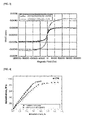
- FIG. 3 is a graph showing the data about the magnetic properties of the substrate according to an embodiment of the present invention. As shown in FIG. 3 , it can be seen that the substrate nearly exhibit nonmagnetic properties at a temperature of 77K.
- FIG. 4 is a graph showing the data about the physical properties of a high-temperature superconducting tape when a conventional hastelloy substrate was used and when the substrate according to an embodiment of the present invention was used (in this case, a high-temperature superconducting layer made of gadolinium barium copper oxide (GdBa 2 Cu 3 O 7 , GBCO) was used). As shown in FIG.
- the elastic modulus of the high-temperature superconducting tape using the stainless steel substrate of the present invention at 77K is 143.6 GPa
- the elastic modulus of the high-temperature superconducting tape using the conventional hastelloy substrate at 77K is 114.3 GPa
- both the yield strength of the substrate of the present invention and the yield strength of the conventional hastelloy substrate are 800 MPa or more.
- FIG. 5 is a graph showing the data about the critical current density of the high-temperature superconducting tape of the present invention (high-temperature superconducting tape of FIG. 4 ). From FIG. 5 , it can be observed that the critical current density of the high-temperature superconducting tape using the stainless steel substrate of the present invention is similar to or higher than that of the high-temperature superconducting tape using the conventional hastelloy substrate. That is, when the conventional hastelloy substrate was used, the critical current density thereof was 450A.
- the critical current density thereof was 575A (a SUS310S substrate was used as the substrate, SUS 1) or 475A (a stainless steel substrate including silicon (Si) 0.5%, molybdenum (Mo) 1%, iron (Fe) 50%, nickel (Ni) 18%, chromium (Cr) 24%, manganese (Mn) 1.5% and residual carbon (C), SUS 2). Consequently, it can be ascertained that the critical current density of the high-temperature superconducting tape using the stainless steel substrate of the present invention is superior to that of the high-temperature superconducting tape using the conventional hastelloy substrate.
- FIG. 6 is a photograph showing the state of the conventional high-temperature superconducting tape which was manufactured by sequentially forming a buffer layer and a superconducting layer on a conventional stainless steel substrate disclosed in US6541121 B2 in the same manner as an embodiment of the present invention and then applying silver (Ag) thereonto to form a protective layer.
- the surface roughness of this conventional high-temperature superconducting tape is higher than that of the high-temperature superconducting tape of the present invention, and, in this case, the silver (Ag) protective layer is easily damaged, thus deteriorating the overall characteristics of the high-temperature superconducting tape.
- the stainless steel substrate is advantageous to electropolishing, the surface roughness thereof is lowered, so that the thickness of the buffer layer or superconducting layer can be reduced and the critical current density of the high-temperature superconducting tape can be improved, thereby improving the overall characteristics of the high-temperature superconducting tape and reducing the manufacturing cost of the high-temperature superconducting tape.
- the high-temperature superconducting tape according to the present invention is advantageous in that a stainless steel substrate obtained by adjusting the composition ratio and metal grain size of the substrate exhibits nonmagnetic properties and is inexpensive compared to a conventional hastelloy substrate, and is easily electroplished compared to a conventional stainless steel substrate, so that the surface roughness thereof is low and thus the thickness of a buffer layer can be reduced, with the result that a high-grade superconducting layer can be deposited on the thin buffer layer and thus the critical current density of the high-temperature superconducting tape can be improved, thereby remarkably improving the characteristics of the high-temperature superconducting tape.
Landscapes
- Engineering & Computer Science (AREA)
- Manufacturing & Machinery (AREA)
- Superconductors And Manufacturing Methods Therefor (AREA)
- Inorganic Compounds Of Heavy Metals (AREA)
Applications Claiming Priority (1)
| Application Number | Priority Date | Filing Date | Title |
|---|---|---|---|
| KR1020110029468A KR20120111137A (ko) | 2011-03-31 | 2011-03-31 | 고온 초전도 선재 |
Publications (3)
| Publication Number | Publication Date |
|---|---|
| EP2506324A2 true EP2506324A2 (de) | 2012-10-03 |
| EP2506324A3 EP2506324A3 (de) | 2014-01-15 |
| EP2506324B1 EP2506324B1 (de) | 2015-04-22 |
Family
ID=45562079
Family Applications (1)
| Application Number | Title | Priority Date | Filing Date |
|---|---|---|---|
| EP20110183039 Active EP2506324B1 (de) | 2011-03-31 | 2011-09-28 | Hochtemperatursupraleitendes Band |
Country Status (5)
| Country | Link |
|---|---|
| US (1) | US8633137B2 (de) |
| EP (1) | EP2506324B1 (de) |
| JP (1) | JP5492159B2 (de) |
| KR (1) | KR20120111137A (de) |
| ES (1) | ES2537443T3 (de) |
Cited By (1)
| Publication number | Priority date | Publication date | Assignee | Title |
|---|---|---|---|---|
| EP3282493A1 (de) * | 2016-08-10 | 2018-02-14 | Theva Dünnschichttechnik GmbH | Hochtemperatur-supraleiter-bandleiter mit edelstahl-substrat |
Families Citing this family (4)
| Publication number | Priority date | Publication date | Assignee | Title |
|---|---|---|---|---|
| WO2016183190A1 (en) | 2015-05-11 | 2016-11-17 | University Of Houston System | Ultra-thin film superconducting tapes |
| CN108963067B (zh) * | 2018-07-27 | 2022-04-29 | 武汉工程大学 | 一种ReBa2Cu3O7-x超导薄膜上制备钉扎层的方法 |
| CN113013318B (zh) * | 2021-03-09 | 2023-07-11 | 傲普(上海)新能源有限公司 | 一种储能用高温超导材料性能提高方法 |
| CN117854829B (zh) * | 2024-02-01 | 2024-11-01 | 中国科学院赣江创新研究院 | 一种中高熵超导材料及其制备方法与应用 |
Citations (2)
| Publication number | Priority date | Publication date | Assignee | Title |
|---|---|---|---|---|
| EP0312015A2 (de) | 1987-10-16 | 1989-04-19 | The Furukawa Electric Co., Ltd. | Körper mit supraleitendem Oxid und dessen Herstellungsverfahren |
| US6541121B2 (en) | 2000-02-01 | 2003-04-01 | Zentrum Fuer Funktionswerkstoffe Gemeinnuetzige Gesellschaft Mbh | Superconducting element |
Family Cites Families (16)
| Publication number | Priority date | Publication date | Assignee | Title |
|---|---|---|---|---|
| US5019555A (en) * | 1988-08-10 | 1991-05-28 | General Atomics | High purity superconducting compositions and methods for their fabrication |
| JP3383799B2 (ja) * | 1993-09-02 | 2003-03-04 | 独立行政法人物質・材料研究機構 | 超電導複合体及びその製造法 |
| JPH087674A (ja) * | 1994-06-20 | 1996-01-12 | Hitachi Chem Co Ltd | 酸化物超電導複合体の製造法 |
| WO1997005669A1 (en) * | 1995-07-26 | 1997-02-13 | Illinois Superconductor Corporation | Method for producing highly textured yttrium barium cuprate for use in waveguides and transmission lines |
| US5964966A (en) * | 1997-09-19 | 1999-10-12 | Lockheed Martin Energy Research Corporation | Method of forming biaxially textured alloy substrates and devices thereon |
| JP4316070B2 (ja) * | 1999-10-07 | 2009-08-19 | 古河電気工業株式会社 | 高強度配向多結晶金属基板および酸化物超電導線材 |
| US20030036483A1 (en) * | 2000-12-06 | 2003-02-20 | Arendt Paul N. | High temperature superconducting thick films |
| JP4716324B2 (ja) * | 2005-12-26 | 2011-07-06 | 古河電気工業株式会社 | 超電導体用基材およびその製造方法 |
| JP2007200870A (ja) * | 2006-01-26 | 2007-08-09 | Ls Cable Ltd | 超伝導ケーブル用基板の製造方法 |
| JP5252792B2 (ja) * | 2006-08-25 | 2013-07-31 | 日本ミクロコーティング株式会社 | 酸化物超伝導体用テープ基材の研磨方法並びに酸化物超伝導体及び酸化物超伝導体用基材 |
| US7879763B2 (en) * | 2006-11-10 | 2011-02-01 | Superpower, Inc. | Superconducting article and method of making |
| JP5049611B2 (ja) * | 2007-02-16 | 2012-10-17 | 日本ミクロコーティング株式会社 | 超電導体用テープ基材の製造方法及びテープ基材 |
| US8195260B2 (en) * | 2008-07-23 | 2012-06-05 | American Superconductor Corporation | Two-sided splice for high temperature superconductor laminated wires |
| JP5227722B2 (ja) * | 2008-09-30 | 2013-07-03 | 株式会社フジクラ | 多結晶薄膜とその製造方法及び酸化物超電導導体 |
| JP5382911B2 (ja) * | 2008-11-12 | 2014-01-08 | 東洋鋼鈑株式会社 | 酸化物超電導線材用金属積層基板の製造方法及び該基板を用いた酸化物超電導線材 |
| JP5448425B2 (ja) * | 2008-11-21 | 2014-03-19 | 公益財団法人国際超電導産業技術研究センター | 超電導膜成膜用基板、超電導線材及びそれらの製造方法 |
-
2011
- 2011-03-31 KR KR1020110029468A patent/KR20120111137A/ko not_active Ceased
- 2011-08-26 JP JP2011184603A patent/JP5492159B2/ja not_active Expired - Fee Related
- 2011-09-07 US US13/226,678 patent/US8633137B2/en active Active
- 2011-09-28 ES ES11183039.4T patent/ES2537443T3/es active Active
- 2011-09-28 EP EP20110183039 patent/EP2506324B1/de active Active
Patent Citations (2)
| Publication number | Priority date | Publication date | Assignee | Title |
|---|---|---|---|---|
| EP0312015A2 (de) | 1987-10-16 | 1989-04-19 | The Furukawa Electric Co., Ltd. | Körper mit supraleitendem Oxid und dessen Herstellungsverfahren |
| US6541121B2 (en) | 2000-02-01 | 2003-04-01 | Zentrum Fuer Funktionswerkstoffe Gemeinnuetzige Gesellschaft Mbh | Superconducting element |
Cited By (1)
| Publication number | Priority date | Publication date | Assignee | Title |
|---|---|---|---|---|
| EP3282493A1 (de) * | 2016-08-10 | 2018-02-14 | Theva Dünnschichttechnik GmbH | Hochtemperatur-supraleiter-bandleiter mit edelstahl-substrat |
Also Published As
| Publication number | Publication date |
|---|---|
| EP2506324B1 (de) | 2015-04-22 |
| US8633137B2 (en) | 2014-01-21 |
| US20120252680A1 (en) | 2012-10-04 |
| ES2537443T3 (es) | 2015-06-08 |
| EP2506324A3 (de) | 2014-01-15 |
| JP5492159B2 (ja) | 2014-05-14 |
| KR20120111137A (ko) | 2012-10-10 |
| JP2012216487A (ja) | 2012-11-08 |
Similar Documents
| Publication | Publication Date | Title |
|---|---|---|
| US7879161B2 (en) | Strong, non-magnetic, cube textured alloy substrates | |
| CN102414764B (zh) | 用于超导线材的基板、超导线材及其制造方法 | |
| JP2002203439A (ja) | テープ状酸化物超電導体 | |
| EP2506324B1 (de) | Hochtemperatursupraleitendes Band | |
| EP1388899A2 (de) | Oxidsupraleiterdraht | |
| JP4316070B2 (ja) | 高強度配向多結晶金属基板および酸化物超電導線材 | |
| JP5757587B2 (ja) | 鉄系超電導材料、及びこれからなる鉄系超電導層、鉄系超電導テープ線材、鉄系超電導線材 | |
| EP0977283B1 (de) | Substratmaterialien für Oxidsupraleiter | |
| Bhattacharjee et al. | Nickel base substrate tapes for coated superconductor applications | |
| CN104662212B (zh) | 用于外延生长的基材、其制造方法、及用于超导线材的基材 | |
| JP4602911B2 (ja) | 希土類系テープ状酸化物超電導体 | |
| US6743533B1 (en) | Oxide superconductor, manufacturing method thereof, and base substrate therefor | |
| JP5950826B2 (ja) | 超電導線材及び超電導線材の製造方法 | |
| JP5330725B2 (ja) | 超電導線材用基板およびその製造方法 | |
| Khlebnikova et al. | Textured tape substrates from binary copper alloys with vanadium and yttrium for the epitaxial deposition of buffer and superconducting layers | |
| JP5939995B2 (ja) | 超電導線材及び超電導線材の製造方法 | |
| PETRISOR | Ni-Cu-Co biaxially textured substrates for YBCO tape fabrication | |
| JP2012018829A (ja) | 超電導線材およびその製造方法 | |
| Rodionov et al. | Institute of Metal Physics, Russian Academy of Sciences | |
| JP2000299026A (ja) | 酸化物超電導導体とその製造方法および酸化物超電導導体用ベース基材 |
Legal Events
| Date | Code | Title | Description |
|---|---|---|---|
| PUAI | Public reference made under article 153(3) epc to a published international application that has entered the european phase |
Free format text: ORIGINAL CODE: 0009012 |
|
| 17P | Request for examination filed |
Effective date: 20110930 |
|
| AK | Designated contracting states |
Kind code of ref document: A2 Designated state(s): AL AT BE BG CH CY CZ DE DK EE ES FI FR GB GR HR HU IE IS IT LI LT LU LV MC MK MT NL NO PL PT RO RS SE SI SK SM TR |
|
| AX | Request for extension of the european patent |
Extension state: BA ME |
|
| PUAL | Search report despatched |
Free format text: ORIGINAL CODE: 0009013 |
|
| AK | Designated contracting states |
Kind code of ref document: A3 Designated state(s): AL AT BE BG CH CY CZ DE DK EE ES FI FR GB GR HR HU IE IS IT LI LT LU LV MC MK MT NL NO PL PT RO RS SE SI SK SM TR |
|
| AX | Request for extension of the european patent |
Extension state: BA ME |
|
| RIC1 | Information provided on ipc code assigned before grant |
Ipc: H01L 39/14 20060101AFI20131212BHEP Ipc: H01L 39/24 20060101ALI20131212BHEP Ipc: H01B 12/06 20060101ALI20131212BHEP |
|
| RBV | Designated contracting states (corrected) |
Designated state(s): AL AT BE BG CH CY CZ DE DK EE ES FI FR GB GR HR HU IE IS IT LI LT LU LV MC MK MT NL NO PL PT RO RS SE SI SK SM TR |
|
| GRAP | Despatch of communication of intention to grant a patent |
Free format text: ORIGINAL CODE: EPIDOSNIGR1 |
|
| INTG | Intention to grant announced |
Effective date: 20141210 |
|
| GRAS | Grant fee paid |
Free format text: ORIGINAL CODE: EPIDOSNIGR3 |
|
| GRAA | (expected) grant |
Free format text: ORIGINAL CODE: 0009210 |
|
| AK | Designated contracting states |
Kind code of ref document: B1 Designated state(s): AL AT BE BG CH CY CZ DE DK EE ES FI FR GB GR HR HU IE IS IT LI LT LU LV MC MK MT NL NO PL PT RO RS SE SI SK SM TR |
|
| REG | Reference to a national code |
Ref country code: GB Ref legal event code: FG4D |
|
| REG | Reference to a national code |
Ref country code: CH Ref legal event code: EP |
|
| REG | Reference to a national code |
Ref country code: AT Ref legal event code: REF Ref document number: 723704 Country of ref document: AT Kind code of ref document: T Effective date: 20150515 |
|
| REG | Reference to a national code |
Ref country code: IE Ref legal event code: FG4D |
|
| REG | Reference to a national code |
Ref country code: DE Ref legal event code: R096 Ref document number: 602011015844 Country of ref document: DE Effective date: 20150528 |
|
| REG | Reference to a national code |
Ref country code: ES Ref legal event code: FG2A Ref document number: 2537443 Country of ref document: ES Kind code of ref document: T3 Effective date: 20150608 |
|
| REG | Reference to a national code |
Ref country code: NL Ref legal event code: VDEP Effective date: 20150422 |
|
| REG | Reference to a national code |
Ref country code: AT Ref legal event code: MK05 Ref document number: 723704 Country of ref document: AT Kind code of ref document: T Effective date: 20150422 |
|
| REG | Reference to a national code |
Ref country code: LT Ref legal event code: MG4D |
|
| PG25 | Lapsed in a contracting state [announced via postgrant information from national office to epo] |
Ref country code: NL Free format text: LAPSE BECAUSE OF FAILURE TO SUBMIT A TRANSLATION OF THE DESCRIPTION OR TO PAY THE FEE WITHIN THE PRESCRIBED TIME-LIMIT Effective date: 20150422 |
|
| PG25 | Lapsed in a contracting state [announced via postgrant information from national office to epo] |
Ref country code: LT Free format text: LAPSE BECAUSE OF FAILURE TO SUBMIT A TRANSLATION OF THE DESCRIPTION OR TO PAY THE FEE WITHIN THE PRESCRIBED TIME-LIMIT Effective date: 20150422 Ref country code: HR Free format text: LAPSE BECAUSE OF FAILURE TO SUBMIT A TRANSLATION OF THE DESCRIPTION OR TO PAY THE FEE WITHIN THE PRESCRIBED TIME-LIMIT Effective date: 20150422 Ref country code: PT Free format text: LAPSE BECAUSE OF FAILURE TO SUBMIT A TRANSLATION OF THE DESCRIPTION OR TO PAY THE FEE WITHIN THE PRESCRIBED TIME-LIMIT Effective date: 20150824 Ref country code: NO Free format text: LAPSE BECAUSE OF FAILURE TO SUBMIT A TRANSLATION OF THE DESCRIPTION OR TO PAY THE FEE WITHIN THE PRESCRIBED TIME-LIMIT Effective date: 20150722 Ref country code: FI Free format text: LAPSE BECAUSE OF FAILURE TO SUBMIT A TRANSLATION OF THE DESCRIPTION OR TO PAY THE FEE WITHIN THE PRESCRIBED TIME-LIMIT Effective date: 20150422 |
|
| PG25 | Lapsed in a contracting state [announced via postgrant information from national office to epo] |
Ref country code: GR Free format text: LAPSE BECAUSE OF FAILURE TO SUBMIT A TRANSLATION OF THE DESCRIPTION OR TO PAY THE FEE WITHIN THE PRESCRIBED TIME-LIMIT Effective date: 20150723 Ref country code: IS Free format text: LAPSE BECAUSE OF FAILURE TO SUBMIT A TRANSLATION OF THE DESCRIPTION OR TO PAY THE FEE WITHIN THE PRESCRIBED TIME-LIMIT Effective date: 20150822 Ref country code: RS Free format text: LAPSE BECAUSE OF FAILURE TO SUBMIT A TRANSLATION OF THE DESCRIPTION OR TO PAY THE FEE WITHIN THE PRESCRIBED TIME-LIMIT Effective date: 20150422 Ref country code: LV Free format text: LAPSE BECAUSE OF FAILURE TO SUBMIT A TRANSLATION OF THE DESCRIPTION OR TO PAY THE FEE WITHIN THE PRESCRIBED TIME-LIMIT Effective date: 20150422 Ref country code: AT Free format text: LAPSE BECAUSE OF FAILURE TO SUBMIT A TRANSLATION OF THE DESCRIPTION OR TO PAY THE FEE WITHIN THE PRESCRIBED TIME-LIMIT Effective date: 20150422 |
|
| REG | Reference to a national code |
Ref country code: DE Ref legal event code: R097 Ref document number: 602011015844 Country of ref document: DE |
|
| PG25 | Lapsed in a contracting state [announced via postgrant information from national office to epo] |
Ref country code: DK Free format text: LAPSE BECAUSE OF FAILURE TO SUBMIT A TRANSLATION OF THE DESCRIPTION OR TO PAY THE FEE WITHIN THE PRESCRIBED TIME-LIMIT Effective date: 20150422 Ref country code: EE Free format text: LAPSE BECAUSE OF FAILURE TO SUBMIT A TRANSLATION OF THE DESCRIPTION OR TO PAY THE FEE WITHIN THE PRESCRIBED TIME-LIMIT Effective date: 20150422 |
|
| PLBE | No opposition filed within time limit |
Free format text: ORIGINAL CODE: 0009261 |
|
| STAA | Information on the status of an ep patent application or granted ep patent |
Free format text: STATUS: NO OPPOSITION FILED WITHIN TIME LIMIT |
|
| PG25 | Lapsed in a contracting state [announced via postgrant information from national office to epo] |
Ref country code: SK Free format text: LAPSE BECAUSE OF FAILURE TO SUBMIT A TRANSLATION OF THE DESCRIPTION OR TO PAY THE FEE WITHIN THE PRESCRIBED TIME-LIMIT Effective date: 20150422 Ref country code: RO Free format text: LAPSE BECAUSE OF NON-PAYMENT OF DUE FEES Effective date: 20150422 Ref country code: PL Free format text: LAPSE BECAUSE OF FAILURE TO SUBMIT A TRANSLATION OF THE DESCRIPTION OR TO PAY THE FEE WITHIN THE PRESCRIBED TIME-LIMIT Effective date: 20150422 Ref country code: CZ Free format text: LAPSE BECAUSE OF FAILURE TO SUBMIT A TRANSLATION OF THE DESCRIPTION OR TO PAY THE FEE WITHIN THE PRESCRIBED TIME-LIMIT Effective date: 20150422 |
|
| 26N | No opposition filed |
Effective date: 20160125 |
|
| PG25 | Lapsed in a contracting state [announced via postgrant information from national office to epo] |
Ref country code: LU Free format text: LAPSE BECAUSE OF FAILURE TO SUBMIT A TRANSLATION OF THE DESCRIPTION OR TO PAY THE FEE WITHIN THE PRESCRIBED TIME-LIMIT Effective date: 20150928 Ref country code: MC Free format text: LAPSE BECAUSE OF FAILURE TO SUBMIT A TRANSLATION OF THE DESCRIPTION OR TO PAY THE FEE WITHIN THE PRESCRIBED TIME-LIMIT Effective date: 20150422 |
|
| REG | Reference to a national code |
Ref country code: CH Ref legal event code: PL |
|
| PG25 | Lapsed in a contracting state [announced via postgrant information from national office to epo] |
Ref country code: SI Free format text: LAPSE BECAUSE OF FAILURE TO SUBMIT A TRANSLATION OF THE DESCRIPTION OR TO PAY THE FEE WITHIN THE PRESCRIBED TIME-LIMIT Effective date: 20150422 |
|
| REG | Reference to a national code |
Ref country code: IE Ref legal event code: MM4A |
|
| PG25 | Lapsed in a contracting state [announced via postgrant information from national office to epo] |
Ref country code: CH Free format text: LAPSE BECAUSE OF NON-PAYMENT OF DUE FEES Effective date: 20150930 Ref country code: LI Free format text: LAPSE BECAUSE OF NON-PAYMENT OF DUE FEES Effective date: 20150930 Ref country code: IE Free format text: LAPSE BECAUSE OF NON-PAYMENT OF DUE FEES Effective date: 20150928 |
|
| PG25 | Lapsed in a contracting state [announced via postgrant information from national office to epo] |
Ref country code: BE Free format text: LAPSE BECAUSE OF FAILURE TO SUBMIT A TRANSLATION OF THE DESCRIPTION OR TO PAY THE FEE WITHIN THE PRESCRIBED TIME-LIMIT Effective date: 20150422 |
|
| REG | Reference to a national code |
Ref country code: FR Ref legal event code: PLFP Year of fee payment: 6 |
|
| PG25 | Lapsed in a contracting state [announced via postgrant information from national office to epo] |
Ref country code: MT Free format text: LAPSE BECAUSE OF FAILURE TO SUBMIT A TRANSLATION OF THE DESCRIPTION OR TO PAY THE FEE WITHIN THE PRESCRIBED TIME-LIMIT Effective date: 20150422 |
|
| PG25 | Lapsed in a contracting state [announced via postgrant information from national office to epo] |
Ref country code: SM Free format text: LAPSE BECAUSE OF FAILURE TO SUBMIT A TRANSLATION OF THE DESCRIPTION OR TO PAY THE FEE WITHIN THE PRESCRIBED TIME-LIMIT Effective date: 20150422 Ref country code: BG Free format text: LAPSE BECAUSE OF FAILURE TO SUBMIT A TRANSLATION OF THE DESCRIPTION OR TO PAY THE FEE WITHIN THE PRESCRIBED TIME-LIMIT Effective date: 20150422 Ref country code: HU Free format text: LAPSE BECAUSE OF FAILURE TO SUBMIT A TRANSLATION OF THE DESCRIPTION OR TO PAY THE FEE WITHIN THE PRESCRIBED TIME-LIMIT; INVALID AB INITIO Effective date: 20110928 |
|
| PG25 | Lapsed in a contracting state [announced via postgrant information from national office to epo] |
Ref country code: CY Free format text: LAPSE BECAUSE OF FAILURE TO SUBMIT A TRANSLATION OF THE DESCRIPTION OR TO PAY THE FEE WITHIN THE PRESCRIBED TIME-LIMIT Effective date: 20150422 Ref country code: SE Free format text: LAPSE BECAUSE OF FAILURE TO SUBMIT A TRANSLATION OF THE DESCRIPTION OR TO PAY THE FEE WITHIN THE PRESCRIBED TIME-LIMIT Effective date: 20150422 |
|
| PG25 | Lapsed in a contracting state [announced via postgrant information from national office to epo] |
Ref country code: TR Free format text: LAPSE BECAUSE OF FAILURE TO SUBMIT A TRANSLATION OF THE DESCRIPTION OR TO PAY THE FEE WITHIN THE PRESCRIBED TIME-LIMIT Effective date: 20150422 |
|
| REG | Reference to a national code |
Ref country code: FR Ref legal event code: PLFP Year of fee payment: 7 |
|
| PG25 | Lapsed in a contracting state [announced via postgrant information from national office to epo] |
Ref country code: MK Free format text: LAPSE BECAUSE OF FAILURE TO SUBMIT A TRANSLATION OF THE DESCRIPTION OR TO PAY THE FEE WITHIN THE PRESCRIBED TIME-LIMIT Effective date: 20150422 |
|
| REG | Reference to a national code |
Ref country code: FR Ref legal event code: PLFP Year of fee payment: 8 |
|
| PG25 | Lapsed in a contracting state [announced via postgrant information from national office to epo] |
Ref country code: AL Free format text: LAPSE BECAUSE OF FAILURE TO SUBMIT A TRANSLATION OF THE DESCRIPTION OR TO PAY THE FEE WITHIN THE PRESCRIBED TIME-LIMIT Effective date: 20150422 |
|
| REG | Reference to a national code |
Ref country code: DE Ref legal event code: R079 Ref document number: 602011015844 Country of ref document: DE Free format text: PREVIOUS MAIN CLASS: H01L0039140000 Ipc: H10N0060200000 |
|
| PGFP | Annual fee paid to national office [announced via postgrant information from national office to epo] |
Ref country code: DE Payment date: 20240918 Year of fee payment: 14 |
|
| PGFP | Annual fee paid to national office [announced via postgrant information from national office to epo] |
Ref country code: GB Payment date: 20240912 Year of fee payment: 14 |
|
| PGFP | Annual fee paid to national office [announced via postgrant information from national office to epo] |
Ref country code: FR Payment date: 20240924 Year of fee payment: 14 |
|
| PGFP | Annual fee paid to national office [announced via postgrant information from national office to epo] |
Ref country code: IT Payment date: 20240913 Year of fee payment: 14 |
|
| PGFP | Annual fee paid to national office [announced via postgrant information from national office to epo] |
Ref country code: ES Payment date: 20241001 Year of fee payment: 14 |