EP2506436B1 - Circuit d'entrée pour un composant d'entrée et procédé de fonctionnement d'un circuit d'entrée - Google Patents
Circuit d'entrée pour un composant d'entrée et procédé de fonctionnement d'un circuit d'entrée Download PDFInfo
- Publication number
- EP2506436B1 EP2506436B1 EP12002230.6A EP12002230A EP2506436B1 EP 2506436 B1 EP2506436 B1 EP 2506436B1 EP 12002230 A EP12002230 A EP 12002230A EP 2506436 B1 EP2506436 B1 EP 2506436B1
- Authority
- EP
- European Patent Office
- Prior art keywords
- circuit
- input
- signal
- reference voltage
- input circuit
- Prior art date
- Legal status (The legal status is an assumption and is not a legal conclusion. Google has not performed a legal analysis and makes no representation as to the accuracy of the status listed.)
- Active
Links
Images



Classifications
-
- H—ELECTRICITY
- H03—ELECTRONIC CIRCUITRY
- H03K—PULSE TECHNIQUE
- H03K19/00—Logic circuits, i.e. having at least two inputs acting on one output; Inverting circuits
- H03K19/0175—Coupling arrangements; Interface arrangements
- H03K19/017545—Coupling arrangements; Impedance matching circuits
- H03K19/017572—Coupling arrangements; Impedance matching circuits using opto-electronic devices
Definitions
- the technical field of the invention relates to an input circuit for an input module for safe reading of an input signal applied to the input module and a method for operating such an input circuit.
- the detection of the zero state is derived from the input voltage by comparing the voltage of the input signal applied from the periphery with an internal reference voltage.
- Such a safe input circuit with a single-channel peripheral connection for the input of a bus subscriber is in the DE 10 2006 030 114 A1 described.
- the in the DE 10 2006 030 114 A1 described input circuit for an input module in particular a bus input module for safe reading of input signals applied to the input module, in particular according to standards Kat.4 DIN EN 954 and SIL 3 IEC 61508, has at least one signal input circuit with a single-channel peripheral connection for connecting at least one signal generator, an evaluation circuit electrically connectable to the signal input circuit via a coupling element and a comparison circuit electrically connected to the signal input circuit for setting a reference voltage for activating and deactivating the coupling element.
- EP 0 393 282 A2 describes an input circuit with an optocoupler to galvanically isolate a control signal from a microprocessor.
- the input circuit comprises a transistor and a zener diode. Once the zener voltage of the zener diode is reached, the zener diode controls a constant current through the transistor. This is possible due to a nearly constant voltage across a resistor connected between an emitter of the transistor and a diode of the optocoupler.
- DE 199 06 932 A1 describes a binary input device 1 with one or more binary input channels, each input channel having a comparator.
- the comparator is set up for a comparison of an input signal which can be applied to a signal input with a reference voltage which can be applied to a reference voltage input.
- GB 2 241 126 A describes input circuits for galvanic isolation of an input signal from an output signal that can be fed to a controller.
- the input circuit includes a rectification circuit, a constant current circuit, and a separation circuit.
- the constant current circuit and a light emitting diode of an opto-coupler of the separation circuit are connected in series at the output of the rectification circuit.
- the constant current circuit has a first resistor, a second resistor, a Zener diode, and a transistor. In this case, the current from the emitter to the collector of the transistor is controlled by a constant voltage at the second resistor and remains constant.
- the input circuit comprises a signal input circuit, a coupling element, an evaluation circuit, a reference voltage circuit and a comparison circuit.
- the signal input circuit has a single-channel peripheral terminal for connecting at least one signal generator, which provides the input signal.
- the evaluation circuit can be coupled to the signal input circuit via a coupling element.
- the reference voltage circuit is electrically connected to the signal input circuit and provides a reference voltage.
- the comparison circuit is coupled between the signal input circuit and the coupling element. The comparison circuit activates and deactivates the coupling element in response to the current of the input signal applied to the signal input circuit and the provided reference voltage.
- an input circuit in which a safe zero state can be detected via both the current of the input signal and the voltage of the input signal. With this input circuit, it is thus ensured that these properties are not lost, even under defined errors, and thus meet the requirements of DIN EN ISO 13849 and DIN EN 61508.
- the comparison circuit has an npn transistor with an adjustable switching threshold determined for the current of the input signal. Further, the comparison circuit comprises a second resistor coupled between the base of the npn transistor and a first resistor of the signal input circuit and a third resistor coupled between the emitter of the npn transistor and ground, the switching threshold passing through 1 R 3 U re f - U BE where R 3 is the third resistor, U Ref is the reference voltage, and U BE is the base-emitter voltage of the npn transistor.
- the transistor activates the coupling element, if the current of the input signal is greater than the switching threshold.
- the transistor deactivates the coupling element if the current of the input signal is less than the switching threshold.
- the triggering or reaching of the adjustable switching threshold determined for the current of the input signal is consequently determined via the current of the input signal.
- a method for operating an input circuit for an input module for safe reading of an input module applied to the input module, wherein the input circuit comprises a signal input circuit having a single-channel peripheral connection for connecting at least one signal generator for providing the input signal and an evaluation circuit which can be coupled to the signal input circuit via a coupling element having.
- the method has a step of providing a reference voltage. Further, the method has a step of activating and deactivating the coupling element in response to the current of the input signal applied to the signal input circuit and the provided reference voltage.
- the comparison circuit is configured to compare the provided reference voltage with a voltage proportional to the current of the input signal for activating and deactivating the coupling element.
- the comparison circuit can activate or deactivate the coupling element.
- the input circuit may comprise means which are suitable for setting the switching threshold. These means can be designed as programmable means.
- the evaluation circuit provides on the output side a digital zero state for the input signal, if the transistor deactivates the coupling element.
- the evaluation circuit can provide on the output side a digital one-state for the input signal.
- the current through the input circuit can be driven exclusively by the input signal applied to the signal input circuit.
- the structure of the input circuit ensures that the current through the input circuit can only be operated by the input signal applied to the signal input circuit.
- the reference voltage circuit is adapted to the Setting threshold by adjusting the reference voltage.
- the voltage for setting the switching threshold for safe detection of the zero state at the input of the input circuit is set via the reference or reference voltage circuit. Only when a voltage V 2 at the emitter of the npn transistor is greater than or equal to a voltage of U Ref - U BE , the transistor blocks and a current can flow through the input of the coupling element.
- the triggering or reaching of the adjustable switching threshold which is determined for the current of the input signal, is consequently determined in turn via the current of the input signal.
- the reference voltage circuit has a zener diode.
- the coupling element is an optocoupler.
- a first test circuit electrically connected to the signal input circuit is provided for testing the comparison circuit and the coupling element.
- the use of the first test circuit makes it possible to check the function of the comparison circuit and the function of the coupling element in order to be able to diagnose possible component failures.
- the test is performed as a dynamic test.
- a limiting unit for limiting the current of the input signal is arranged between the signal input circuit and the comparison circuit.
- the limiting unit is, for example, a current limiting unit which has a zener diode.
- the current limiting unit is in particular configured to reduce the power loss of the input circuit.
- a second test circuit which is electrically connected to the reference voltage circuit, is provided for testing the reference voltage provided by the reference voltage circuit.
- the test by the second test circuit or test unit is preferably performed as a dynamic test.
- the second test circuit is arranged to increase the self-diagnosis of the input circuit to allow the reference to determine the switching threshold determining reference.
- an input module which has at least one input circuit as explained above for the safe reading in of an input signal applied to the input module.
- the input module has a plurality of input circuits, a single reference voltage circuit for providing a reference voltage and a single second test circuit for testing the reference voltage circuit.
- a single reference voltage circuit suffices for the provision of reference voltages for the majority of the input circuits.
- a single second test circuit for testing the reference voltage circuit suffices here.
- FIG. 1 is a schematic block diagram of a first embodiment of an input circuit 100 for reading an applied input signal shown.
- the input circuit 100 has a signal input circuit 110, an evaluation circuit 120, a comparison circuit 130, a reference voltage circuit 140 and a coupling element IC1.
- the signal input circuit 110 has a single-channel peripheral terminal for connecting at least one signal generator for providing the input signal INO.
- the signal input circuit 110 has a first resistor R 1 .
- the coupling element IC1 couples the signal input circuit 110 to the evaluation circuit 120.
- the coupling element IC1 is designed, for example, as an opto-coupler.
- the reference voltage circuit 140 is electrically connected to provide a reference voltage U Ref .
- the reference voltage circuit 140 is formed, for example, by a zener diode.
- the comparison circuit 130 is coupled between the signal input circuit 110 and the coupling element IC1.
- the comparison circuit 130 may activate and deactivate the coupling element IC1 in response to the current of the input signal INO applied to the signal input circuit 110 and the provided reference voltage U Ref .
- the comparison circuit 130 compares the reference voltage U ref to meet at a rate proportional to the current of the input signal INO voltage, the decision on the activation or deactivation of the coupling element IC1.
- the comparison circuit 130 has, in particular, an npn transistor with an adjustable switching threshold determined for the current of the input signal INO.
- the triggering or reaching of the adjustable switching threshold is determined by the current of the input signal.
- the npn transistor 130 activates the coupling element IC1 when the current of the input signal INO is greater than the switching threshold.
- the npn transistor 130 deactivates the coupling element IC1 when the current of the input signal INO is smaller than the switching threshold.
- the switching threshold is determined by 1 R 3 U re f - U BE . where R 3 denotes the third resistor, U Ref the reference voltage and U BE the base-emitter voltage of the npn transistor 130.
- the structure of the input circuit 100 is shown in FIG. 1 such that the current through the input circuit 100 can be driven only by the input signal INO.
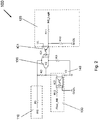
- FIG. 2 shows a schematic block diagram of a second embodiment of an input circuit 100 for safe reading of an applied input signal INO.
- the second embodiment of the FIG. 2 as well as the further embodiments of the Figures 3 and 4 are based on the first embodiment of the FIG. 1 and have all the features of the first embodiment. In order to avoid repetition, the matching characteristics with respect to the Figures 2 . 3 and 4 not explained again.
- the input circuit 100 of FIG. 2 has with respect to the input circuit 100 of FIG. 1 additionally a first test circuit 150 for testing the comparison circuit 130 and the coupling element IC1.
- the first test circuit 150 is electrically connected to the signal input circuit 110.
- the first test circuit 150 has a second coupling element IC2 and a resistor R 12 .
- the first test circuit 150 is configured to check for possible component failures of the comparison circuit 130 and of the coupling element IC1.
- the signal / Test_INO which is set in normal operation, is switched off for a short time. This causes transistor 130 to take over the current flow. As a result, no current can be driven through the coupling member IC1 more.
- the forced test-wise change of the signal INO_Logik at the output of the evaluation circuit 120 can be evaluated by a downstream logic unit.
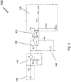
- FIG. 3 is a schematic block diagram of a third embodiment of an input circuit 100 for safe reading of an applied input signal INO mapped.
- the third embodiment of the input circuit 100 according to FIG. 3 has in addition to the first embodiment of FIG. 1 a limiting unit 160 for limiting the current of the input signal INO.
- the limiting unit 160 is coupled between the signal input circuit 110 and the comparison circuit 130.
- limiting unit 160 or current limiting unit of the input current of the input circuit 100 is limited from a voltage adjustable by the Zener diode V4 of the limiting unit 160 voltage. This leads to the reduction of the power loss.
- FIG. 4 is a schematic block diagram of a fourth embodiment of an input circuit 100 for safe reading of an applied input signal shown.
- the fourth embodiment of the input circuit 100 is compared to the first embodiment of FIG. 1 expanded so that a second test circuit 170 is provided.
- the second test circuit 170 is electrically connected to the reference voltage circuit 140 and is for testing that provided by the reference voltage circuit 140 Reference voltage U Ref set up.
- the signal Test_Ref is set from a preformed logic unit, whereby the voltage of the reference voltage circuit 140 is switched to a comparator of the second test circuit 170, in which it is compared with a further reference voltage.
- the result of this comparison is transmitted via a further coupling element IC21 of the logic unit and evaluated by this.
- the further coupling element IC21 can be designed as an opto-coupler.
- FIG. 2 shows a schematic block diagram of an input module 500 with two input circuits 101, 102.
- the input module 500 has a first input circuit 101 and a second input circuit 102.
- the input module may also have more than two input circuits.
- the first input circuit 101 and the second input circuit 102 are coupled to a single reference voltage circuit 140.
- This single reference voltage circuit provides a reference voltage for the first input circuit 101 and the second input circuit 102.
- a single second test circuit 170 is provided for testing the one reference voltage circuit 140.
- FIG. 6 is a schematic flow diagram of an embodiment of a method for operating an input circuit for safe reading of an adjacent Input signal shown. Examples of such an input circuit are in the Fig. 1 to 4 shown.
- the input circuit has a signal input circuit with a single-channel peripheral connection for connecting at least one signal generator for providing the input signal and an evaluation circuit which can be coupled to the signal input circuit via a coupling element.
- step 601 a reference voltage is provided.
- step 602 the coupling element is activated or deactivated in response to the current of the input signal applied to the signal input circuit and the provided reference voltage.
Landscapes
- Engineering & Computer Science (AREA)
- Computer Hardware Design (AREA)
- Physics & Mathematics (AREA)
- Computing Systems (AREA)
- General Engineering & Computer Science (AREA)
- Mathematical Physics (AREA)
- Logic Circuits (AREA)
Claims (13)
- Circuit d'entrée (100) destiné à un module d'entrée pour la lecture fiable d'un signal d'entrée (INO) s'appliquant contre le module d'entrée, comprenant :un circuit d'entrée de signal (110) comprenant un raccord périphérique à un canal pour le raccordement d'au moins un générateur de signaux destiné à fournir le signal d'entrée (INO),un circuit d'évaluation (120) pouvant être couplé au circuit d'entrée de signal (110) par un élément de couplage (IC1),un circuit de tension de référence (140) relié électriquement au circuit d'entrée de signal (110) et destiné à fournir une tension de référence (URef) etun circuit de comparaison (130) couplé entre le circuit d'entrée de signal (110) et l'élément de couplage (IC1) pour l'activation et la désactivation de l'élément de couplage (IC1) en fonction du courant du signal d'entrée (INO) s'appliquant contre le circuit d'entrée de signal (110) et de la tension de référence (URef),le circuit de comparaison (130) comprenant un transistor npn à seuil de commutation réglable déterminé pour le courant du signal d'entrée (INO), le transistor npn activant l'élément de couplage (IC1) au cas où le courant du signal d'entrée (INO) serait supérieur au seuil de commutation et le transistor npn désactivant l'élément de couplage (IC1) au cas où le courant du signal d'entrée (INO) serait inférieur au seuil de commutation etle circuit de comparaison (130) comprenant une deuxième résistance (R2) couplée entre la base du transistor npn et une première résistance (R1) du circuit d'entrée de signal (110), et le circuit de comparaison (130) comprend une troisième résistance (R3) couplée entre l'émetteur du transistor npn et la masse,de sorte que le seuil de commutation est égal à

- Circuit d'entrée (100) selon la revendication 1, caractérisé en ce que le circuit de comparaison (130) est conçu pour comparer la tension de référence (URef) fournie à une tension proportionnelle au courant du signal d'entrée (INO) pour l'activation et la désactivation de l'élément de couplage (IC1).
- Circuit d'entrée (100) selon la revendication 1 ou 2, caractérisé en ce que le circuit d'évaluation (120) fournit côté sortie un état zéro numérique pour le signal d'entrée (INO) au cas où le transistor npn désactiverait l'élément de couplage (IC1).
- Circuit d'entrée (100) selon l'une quelconque des revendications précédentes, caractérisé en ce que le courant traversant le circuit d'entrée (100) peut être commandé exclusivement par le signal d'entrée (INO) s'appliquant contre le circuit d'entrée de signal (110).
- Circuit d'entrée (100) selon l'une quelconque des revendications précédentes, caractérisé en ce que le circuit de tension de référence (140) est conçu pour régler le seuil de commutation par réglage de la tension de référence.
- Circuit d'entrée (100) selon l'une quelconque des revendications précédentes, caractérisé en ce que le circuit de tension de référence (140) comprend une diode Zener.
- Circuit d'entrée (100) selon l'une quelconque des revendications précédentes, caractérisé en ce que l'élément de couplage (IC1) est un optocoupleur.
- Circuit d'entrée (100) selon l'une quelconque des revendications précédentes, caractérisé en ce qu'un premier circuit d'essai (150) relié électriquement au circuit d'entrée de signal (110) est destiné à tester le circuit de comparaison (130) et l'élément de couplage (IC1).
- Circuit d'entrée (100) selon l'une quelconque des revendications précédentes, caractérisé en ce qu'une unité de limitation (160) destinée à limiter le courant du signal d'entrée (INO) est agencée entre le circuit d'entrée de signal (110) et le circuit de comparaison (130).
- Circuit d'entrée (100) selon l'une quelconque des revendications précédentes, caractérisé en ce qu'un deuxième circuit d'essai (170) relié électriquement au circuit de tension de référence (140) et destiné à tester la tension de référence (URef) fournie par le circuit de tension de référence (140) est prévu.
- Module d'entrée (500), comprenant :au moins un circuit d'entrée (100, 101, 102) pour la lecture fiable d'un signal d'entrée s'appliquant contre le module d'entrée selon l'une quelconque des revendications précédentes.
- Module d'entrée (500) selon la revendication 11, caractérisé en ce qu'une pluralité de circuits d'entrée (100, 101, 102) selon l'une des revendications 1 à 11, un seul circuit de tension de référence (140) destiné à fournir une tension de référence (URef) et un seul deuxième circuit d'essai (170) destiné à tester le circuit de tension de référence (140) sont prévus.
- Procédé permettant de faire fonctionner un circuit d'entrée (100) destiné à un module d'entrée pour la lecture fiable d'un signal d'entrée (INO) s'appliquant contre le module d'entrée, le circuit d'entrée (100) comprenant un circuit d'entrée de signal (110) comprenant un raccord périphérique à un canal pour le raccordement d'au moins un générateur de signaux destiné à fournir le signal d'entrée (INO) et un circuit d'évaluation (120) pouvant être couplé au circuit d'entrée de signal (110) par un élément de couplage (IC1),
et le circuit d'entrée (100) comprenant un circuit de comparaison (130) pourvu d'un transistor npn à seuil de commutation réglable déterminé pour le courant du signal d'entrée (INO), une deuxième résistance (R2) couplée entre la base du transistor npn et une première résistance (R1) du circuit d'entrée de signal (110) et une troisième résistance (R3) couplée entre l'émetteur du transistor npn et la masse,
comprenant les étapes consistant à :fournir (601) une tension de référence (URef) dans un circuit de tension de référence (140) qui est relié électriquement au circuit d'entrée de signal (110), etactiver et désactiver (602) l'élément de couplage (IC1) en fonction du courant du signal d'entrée (INO) s'appliquant contre le circuit d'entrée de signal (110) et de la tension de référence (URef) fournie, de sorte que le seuil de commutation est égal à
Applications Claiming Priority (1)
| Application Number | Priority Date | Filing Date | Title |
|---|---|---|---|
| DE102011015498A DE102011015498B4 (de) | 2011-03-29 | 2011-03-29 | Eingangsschaltung für eine Eingangsbaugruppe und Verfahren zum Betreiben einer Eingangsschaltung |
Publications (3)
| Publication Number | Publication Date |
|---|---|
| EP2506436A2 EP2506436A2 (fr) | 2012-10-03 |
| EP2506436A3 EP2506436A3 (fr) | 2013-05-22 |
| EP2506436B1 true EP2506436B1 (fr) | 2018-04-18 |
Family
ID=46000615
Family Applications (1)
| Application Number | Title | Priority Date | Filing Date |
|---|---|---|---|
| EP12002230.6A Active EP2506436B1 (fr) | 2011-03-29 | 2012-03-28 | Circuit d'entrée pour un composant d'entrée et procédé de fonctionnement d'un circuit d'entrée |
Country Status (2)
| Country | Link |
|---|---|
| EP (1) | EP2506436B1 (fr) |
| DE (1) | DE102011015498B4 (fr) |
Families Citing this family (8)
| Publication number | Priority date | Publication date | Assignee | Title |
|---|---|---|---|---|
| EP2770637B1 (fr) * | 2013-02-22 | 2015-08-19 | Siemens Aktiengesellschaft | Agencement d'optocoupleur et groupe d'entrée et/ou sortie |
| DE102013106739A1 (de) | 2013-06-27 | 2014-12-31 | Pilz Gmbh & Co. Kg | Sicherheitsschaltvorrichtung mit fehlersicheren Eingängen |
| CN104716950B (zh) * | 2015-03-02 | 2018-05-22 | 苏州市职业大学 | 一种多功能信号输入隔离电路 |
| DE102017131200B4 (de) * | 2017-12-22 | 2019-09-05 | Pilz Gmbh & Co. Kg | Digitale Eingangsschaltung zum Empfangen digitaler Eingangssignale eines Signalgebers |
| DE102019114460A1 (de) * | 2019-05-29 | 2020-12-03 | Pilz Gmbh & Co. Kg | Digitale Eingangsschaltung zum Empfangen digitaler Eingangssignale zumindest eines Signalgebers |
| FR3103914A1 (fr) * | 2019-11-28 | 2021-06-04 | Schneider Electric Industries Sas | Dispositif de commande sécurisée, contacteur comportant un tel dispositif et procédé de traitement sécurisé d’un signal de commande |
| DE102020203653A1 (de) | 2020-03-20 | 2021-09-23 | Festo Se & Co. Kg | Eingangsvorrichtung, Steuerungsgerät und Verfahren zum Betrieb einer Eingangsvorrichtung |
| CN112311382B (zh) * | 2020-10-24 | 2024-08-16 | 浙江华博文化科技股份有限公司 | 一种多导信号耦合器 |
Citations (1)
| Publication number | Priority date | Publication date | Assignee | Title |
|---|---|---|---|---|
| US4788458A (en) * | 1987-07-15 | 1988-11-29 | Rockwell International Corporation | Two wire interface circuit |
Family Cites Families (5)
| Publication number | Priority date | Publication date | Assignee | Title |
|---|---|---|---|---|
| JPS57185725A (en) * | 1981-05-12 | 1982-11-16 | Fuji Electric Co Ltd | Signal input circuit |
| US5068545A (en) * | 1989-04-20 | 1991-11-26 | Elsag International B.V. | Digital/frequency input for industrial control applications |
| JPH03217904A (ja) * | 1990-01-23 | 1991-09-25 | Toshiba Mach Co Ltd | 入力モジュール |
| DE19906932B4 (de) * | 1999-02-19 | 2010-04-22 | Abb Ag | Binäreingabegerät |
| DE102006030114B4 (de) | 2006-06-28 | 2010-09-09 | Phoenix Contact Gmbh & Co. Kg | Sichere Eingangsschaltung mit einkanaligem Peripherieanschluss für den Eingang eines Busteilnehmers |
-
2011
- 2011-03-29 DE DE102011015498A patent/DE102011015498B4/de not_active Expired - Fee Related
-
2012
- 2012-03-28 EP EP12002230.6A patent/EP2506436B1/fr active Active
Patent Citations (1)
| Publication number | Priority date | Publication date | Assignee | Title |
|---|---|---|---|---|
| US4788458A (en) * | 1987-07-15 | 1988-11-29 | Rockwell International Corporation | Two wire interface circuit |
Also Published As
| Publication number | Publication date |
|---|---|
| EP2506436A3 (fr) | 2013-05-22 |
| DE102011015498B4 (de) | 2012-10-25 |
| DE102011015498A1 (de) | 2012-10-04 |
| EP2506436A2 (fr) | 2012-10-03 |
Similar Documents
| Publication | Publication Date | Title |
|---|---|---|
| DE102011015498B4 (de) | Eingangsschaltung für eine Eingangsbaugruppe und Verfahren zum Betreiben einer Eingangsschaltung | |
| DE102019121794A1 (de) | Intelligenter elektronischer schalter | |
| DE102007008097B4 (de) | Lastabnormitäts-Detektionssystem und -verfahren | |
| WO2014009207A1 (fr) | Dispositif de diagnostic d'une circuiterie | |
| WO2005062012A1 (fr) | Dispositif de mesure, en particulier convertisseur de mesure de temperature | |
| DE102020131060A1 (de) | Intelligenter elektronischer schalter | |
| EP1873915B1 (fr) | Circuit d'entrée sécurisé doté d'un raccordement périphérique sur un canal unique pour l'entrée d'un utilisateur de bus | |
| DE4307794C2 (de) | Einrichtung zur Überwachung symmetrischer Zweidraht-Busleitungen und -Busschnittstellen | |
| DE102016116426B4 (de) | Verfahren zum Verarbeiten eines Single-Edge-Nibble-Transmission-Signals, Datenempfangsvorrichtung und Datenübertragungseinrichtung | |
| DE112012006739T5 (de) | Ein-/Ausgangs-Multiplex-Port und Steuergerät | |
| DE102014219130B4 (de) | Diagnoseschaltung und Verfahren zum Betreiben einer Diagnoseschaltung | |
| WO2009097922A1 (fr) | Procédé pour contrôler au moins une bougie-crayon de préchauffage d'un moteur à combustion interne et dispositif correspondant | |
| WO2017076572A1 (fr) | Système de bus et procédé de diagnostic d'un court-circuit | |
| DE10127054A1 (de) | Verfahren zur Überwachung einer Spannungsversorgung eines Steuergeräts in einem Kraftfahrzeug | |
| DE102005016291A1 (de) | Differenzverstärkerschaltung | |
| DE102018206804A1 (de) | Erkennung von Unterbrechungen eines Stromkreises | |
| EP2713680B1 (fr) | Méthode pour la détermination de la disponibilité d'une ligne de bus et unité de contrôle de communication | |
| EP3665869A1 (fr) | Dispositif d'émission/réception pour systeme de bus et procédé de réduction de la tendance à osciller entre differents états binaires | |
| DE102020112985A1 (de) | IO-Link-Adapter | |
| DE102007036680B4 (de) | Schaltungsvorrichtung zur Erkennung einer unterbrochenen Masseleitung | |
| DE10111468B4 (de) | Verfahren und Vorrichtung zur Ermittlung von Eigenschaften gesteckter Module | |
| EP1285489A2 (fr) | Circuit avec disjoncteur | |
| DE102008018842B4 (de) | Verfahren und Schnittstelle zur Kommunikation eines Steuergeräts über eine bidirektionale Leitung | |
| WO2005101345A1 (fr) | Transducteur de mesure numerique a signal de courant | |
| DE102025128618A1 (de) | Versorgung von elektrischen Verbrauchern in einem Fahrzeug mit elektrischer Energie und Schutz der Verbraucher und/oder ihres Versorgungsleitungsnetzwerks vor Überlast |
Legal Events
| Date | Code | Title | Description |
|---|---|---|---|
| PUAI | Public reference made under article 153(3) epc to a published international application that has entered the european phase |
Free format text: ORIGINAL CODE: 0009012 |
|
| 17P | Request for examination filed |
Effective date: 20120405 |
|
| AK | Designated contracting states |
Kind code of ref document: A2 Designated state(s): AL AT BE BG CH CY CZ DE DK EE ES FI FR GB GR HR HU IE IS IT LI LT LU LV MC MK MT NL NO PL PT RO RS SE SI SK SM TR |
|
| AX | Request for extension of the european patent |
Extension state: BA ME |
|
| PUAL | Search report despatched |
Free format text: ORIGINAL CODE: 0009013 |
|
| AK | Designated contracting states |
Kind code of ref document: A3 Designated state(s): AL AT BE BG CH CY CZ DE DK EE ES FI FR GB GR HR HU IE IS IT LI LT LU LV MC MK MT NL NO PL PT RO RS SE SI SK SM TR |
|
| AX | Request for extension of the european patent |
Extension state: BA ME |
|
| RIC1 | Information provided on ipc code assigned before grant |
Ipc: H03K 19/0175 20060101AFI20130417BHEP |
|
| 17Q | First examination report despatched |
Effective date: 20131031 |
|
| RBV | Designated contracting states (corrected) |
Designated state(s): AL AT BE BG CH CY CZ DE DK EE ES FI FR GB GR HR HU IE IS IT LI LT LU LV MC MK MT NL NO PL PT RO RS SE SI SK SM TR |
|
| GRAP | Despatch of communication of intention to grant a patent |
Free format text: ORIGINAL CODE: EPIDOSNIGR1 |
|
| STAA | Information on the status of an ep patent application or granted ep patent |
Free format text: STATUS: GRANT OF PATENT IS INTENDED |
|
| INTG | Intention to grant announced |
Effective date: 20171120 |
|
| GRAS | Grant fee paid |
Free format text: ORIGINAL CODE: EPIDOSNIGR3 |
|
| GRAA | (expected) grant |
Free format text: ORIGINAL CODE: 0009210 |
|
| STAA | Information on the status of an ep patent application or granted ep patent |
Free format text: STATUS: THE PATENT HAS BEEN GRANTED |
|
| AK | Designated contracting states |
Kind code of ref document: B1 Designated state(s): AL AT BE BG CH CY CZ DE DK EE ES FI FR GB GR HR HU IE IS IT LI LT LU LV MC MK MT NL NO PL PT RO RS SE SI SK SM TR |
|
| REG | Reference to a national code |
Ref country code: GB Ref legal event code: FG4D Free format text: NOT ENGLISH |
|
| REG | Reference to a national code |
Ref country code: CH Ref legal event code: EP |
|
| REG | Reference to a national code |
Ref country code: DE Ref legal event code: R096 Ref document number: 502012012533 Country of ref document: DE |
|
| REG | Reference to a national code |
Ref country code: AT Ref legal event code: REF Ref document number: 991496 Country of ref document: AT Kind code of ref document: T Effective date: 20180515 |
|
| REG | Reference to a national code |
Ref country code: IE Ref legal event code: FG4D Free format text: LANGUAGE OF EP DOCUMENT: GERMAN |
|
| REG | Reference to a national code |
Ref country code: NL Ref legal event code: MP Effective date: 20180418 |
|
| REG | Reference to a national code |
Ref country code: LT Ref legal event code: MG4D |
|
| PG25 | Lapsed in a contracting state [announced via postgrant information from national office to epo] |
Ref country code: NL Free format text: LAPSE BECAUSE OF FAILURE TO SUBMIT A TRANSLATION OF THE DESCRIPTION OR TO PAY THE FEE WITHIN THE PRESCRIBED TIME-LIMIT Effective date: 20180418 |
|
| PG25 | Lapsed in a contracting state [announced via postgrant information from national office to epo] |
Ref country code: PL Free format text: LAPSE BECAUSE OF FAILURE TO SUBMIT A TRANSLATION OF THE DESCRIPTION OR TO PAY THE FEE WITHIN THE PRESCRIBED TIME-LIMIT Effective date: 20180418 Ref country code: NO Free format text: LAPSE BECAUSE OF FAILURE TO SUBMIT A TRANSLATION OF THE DESCRIPTION OR TO PAY THE FEE WITHIN THE PRESCRIBED TIME-LIMIT Effective date: 20180718 Ref country code: LT Free format text: LAPSE BECAUSE OF FAILURE TO SUBMIT A TRANSLATION OF THE DESCRIPTION OR TO PAY THE FEE WITHIN THE PRESCRIBED TIME-LIMIT Effective date: 20180418 Ref country code: ES Free format text: LAPSE BECAUSE OF FAILURE TO SUBMIT A TRANSLATION OF THE DESCRIPTION OR TO PAY THE FEE WITHIN THE PRESCRIBED TIME-LIMIT Effective date: 20180418 Ref country code: AL Free format text: LAPSE BECAUSE OF FAILURE TO SUBMIT A TRANSLATION OF THE DESCRIPTION OR TO PAY THE FEE WITHIN THE PRESCRIBED TIME-LIMIT Effective date: 20180418 Ref country code: SE Free format text: LAPSE BECAUSE OF FAILURE TO SUBMIT A TRANSLATION OF THE DESCRIPTION OR TO PAY THE FEE WITHIN THE PRESCRIBED TIME-LIMIT Effective date: 20180418 Ref country code: BG Free format text: LAPSE BECAUSE OF FAILURE TO SUBMIT A TRANSLATION OF THE DESCRIPTION OR TO PAY THE FEE WITHIN THE PRESCRIBED TIME-LIMIT Effective date: 20180718 Ref country code: FI Free format text: LAPSE BECAUSE OF FAILURE TO SUBMIT A TRANSLATION OF THE DESCRIPTION OR TO PAY THE FEE WITHIN THE PRESCRIBED TIME-LIMIT Effective date: 20180418 |
|
| PG25 | Lapsed in a contracting state [announced via postgrant information from national office to epo] |
Ref country code: LV Free format text: LAPSE BECAUSE OF FAILURE TO SUBMIT A TRANSLATION OF THE DESCRIPTION OR TO PAY THE FEE WITHIN THE PRESCRIBED TIME-LIMIT Effective date: 20180418 Ref country code: RS Free format text: LAPSE BECAUSE OF FAILURE TO SUBMIT A TRANSLATION OF THE DESCRIPTION OR TO PAY THE FEE WITHIN THE PRESCRIBED TIME-LIMIT Effective date: 20180418 Ref country code: GR Free format text: LAPSE BECAUSE OF FAILURE TO SUBMIT A TRANSLATION OF THE DESCRIPTION OR TO PAY THE FEE WITHIN THE PRESCRIBED TIME-LIMIT Effective date: 20180719 Ref country code: HR Free format text: LAPSE BECAUSE OF FAILURE TO SUBMIT A TRANSLATION OF THE DESCRIPTION OR TO PAY THE FEE WITHIN THE PRESCRIBED TIME-LIMIT Effective date: 20180418 |
|
| PG25 | Lapsed in a contracting state [announced via postgrant information from national office to epo] |
Ref country code: PT Free format text: LAPSE BECAUSE OF FAILURE TO SUBMIT A TRANSLATION OF THE DESCRIPTION OR TO PAY THE FEE WITHIN THE PRESCRIBED TIME-LIMIT Effective date: 20180820 |
|
| REG | Reference to a national code |
Ref country code: DE Ref legal event code: R097 Ref document number: 502012012533 Country of ref document: DE |
|
| PG25 | Lapsed in a contracting state [announced via postgrant information from national office to epo] |
Ref country code: DK Free format text: LAPSE BECAUSE OF FAILURE TO SUBMIT A TRANSLATION OF THE DESCRIPTION OR TO PAY THE FEE WITHIN THE PRESCRIBED TIME-LIMIT Effective date: 20180418 Ref country code: EE Free format text: LAPSE BECAUSE OF FAILURE TO SUBMIT A TRANSLATION OF THE DESCRIPTION OR TO PAY THE FEE WITHIN THE PRESCRIBED TIME-LIMIT Effective date: 20180418 Ref country code: SK Free format text: LAPSE BECAUSE OF FAILURE TO SUBMIT A TRANSLATION OF THE DESCRIPTION OR TO PAY THE FEE WITHIN THE PRESCRIBED TIME-LIMIT Effective date: 20180418 Ref country code: CZ Free format text: LAPSE BECAUSE OF FAILURE TO SUBMIT A TRANSLATION OF THE DESCRIPTION OR TO PAY THE FEE WITHIN THE PRESCRIBED TIME-LIMIT Effective date: 20180418 Ref country code: RO Free format text: LAPSE BECAUSE OF FAILURE TO SUBMIT A TRANSLATION OF THE DESCRIPTION OR TO PAY THE FEE WITHIN THE PRESCRIBED TIME-LIMIT Effective date: 20180418 |
|
| PLBE | No opposition filed within time limit |
Free format text: ORIGINAL CODE: 0009261 |
|
| STAA | Information on the status of an ep patent application or granted ep patent |
Free format text: STATUS: NO OPPOSITION FILED WITHIN TIME LIMIT |
|
| PG25 | Lapsed in a contracting state [announced via postgrant information from national office to epo] |
Ref country code: SM Free format text: LAPSE BECAUSE OF FAILURE TO SUBMIT A TRANSLATION OF THE DESCRIPTION OR TO PAY THE FEE WITHIN THE PRESCRIBED TIME-LIMIT Effective date: 20180418 |
|
| 26N | No opposition filed |
Effective date: 20190121 |
|
| PG25 | Lapsed in a contracting state [announced via postgrant information from national office to epo] |
Ref country code: SI Free format text: LAPSE BECAUSE OF FAILURE TO SUBMIT A TRANSLATION OF THE DESCRIPTION OR TO PAY THE FEE WITHIN THE PRESCRIBED TIME-LIMIT Effective date: 20180418 |
|
| PG25 | Lapsed in a contracting state [announced via postgrant information from national office to epo] |
Ref country code: MC Free format text: LAPSE BECAUSE OF FAILURE TO SUBMIT A TRANSLATION OF THE DESCRIPTION OR TO PAY THE FEE WITHIN THE PRESCRIBED TIME-LIMIT Effective date: 20180418 |
|
| REG | Reference to a national code |
Ref country code: CH Ref legal event code: PL |
|
| GBPC | Gb: european patent ceased through non-payment of renewal fee |
Effective date: 20190328 |
|
| PG25 | Lapsed in a contracting state [announced via postgrant information from national office to epo] |
Ref country code: LU Free format text: LAPSE BECAUSE OF NON-PAYMENT OF DUE FEES Effective date: 20190328 |
|
| REG | Reference to a national code |
Ref country code: BE Ref legal event code: MM Effective date: 20190331 |
|
| PG25 | Lapsed in a contracting state [announced via postgrant information from national office to epo] |
Ref country code: CH Free format text: LAPSE BECAUSE OF NON-PAYMENT OF DUE FEES Effective date: 20190331 Ref country code: GB Free format text: LAPSE BECAUSE OF NON-PAYMENT OF DUE FEES Effective date: 20190328 Ref country code: IE Free format text: LAPSE BECAUSE OF NON-PAYMENT OF DUE FEES Effective date: 20190328 Ref country code: LI Free format text: LAPSE BECAUSE OF NON-PAYMENT OF DUE FEES Effective date: 20190331 |
|
| PG25 | Lapsed in a contracting state [announced via postgrant information from national office to epo] |
Ref country code: BE Free format text: LAPSE BECAUSE OF NON-PAYMENT OF DUE FEES Effective date: 20190331 |
|
| PG25 | Lapsed in a contracting state [announced via postgrant information from national office to epo] |
Ref country code: TR Free format text: LAPSE BECAUSE OF FAILURE TO SUBMIT A TRANSLATION OF THE DESCRIPTION OR TO PAY THE FEE WITHIN THE PRESCRIBED TIME-LIMIT Effective date: 20180418 |
|
| PG25 | Lapsed in a contracting state [announced via postgrant information from national office to epo] |
Ref country code: MT Free format text: LAPSE BECAUSE OF FAILURE TO SUBMIT A TRANSLATION OF THE DESCRIPTION OR TO PAY THE FEE WITHIN THE PRESCRIBED TIME-LIMIT Effective date: 20180418 |
|
| PG25 | Lapsed in a contracting state [announced via postgrant information from national office to epo] |
Ref country code: CY Free format text: LAPSE BECAUSE OF FAILURE TO SUBMIT A TRANSLATION OF THE DESCRIPTION OR TO PAY THE FEE WITHIN THE PRESCRIBED TIME-LIMIT Effective date: 20180418 |
|
| PG25 | Lapsed in a contracting state [announced via postgrant information from national office to epo] |
Ref country code: IS Free format text: LAPSE BECAUSE OF FAILURE TO SUBMIT A TRANSLATION OF THE DESCRIPTION OR TO PAY THE FEE WITHIN THE PRESCRIBED TIME-LIMIT Effective date: 20180818 |
|
| PG25 | Lapsed in a contracting state [announced via postgrant information from national office to epo] |
Ref country code: HU Free format text: LAPSE BECAUSE OF FAILURE TO SUBMIT A TRANSLATION OF THE DESCRIPTION OR TO PAY THE FEE WITHIN THE PRESCRIBED TIME-LIMIT; INVALID AB INITIO Effective date: 20120328 |
|
| PGFP | Annual fee paid to national office [announced via postgrant information from national office to epo] |
Ref country code: AT Payment date: 20220318 Year of fee payment: 11 |
|
| PG25 | Lapsed in a contracting state [announced via postgrant information from national office to epo] |
Ref country code: MK Free format text: LAPSE BECAUSE OF FAILURE TO SUBMIT A TRANSLATION OF THE DESCRIPTION OR TO PAY THE FEE WITHIN THE PRESCRIBED TIME-LIMIT Effective date: 20180418 |
|
| P01 | Opt-out of the competence of the unified patent court (upc) registered |
Effective date: 20230424 |
|
| REG | Reference to a national code |
Ref country code: AT Ref legal event code: MM01 Ref document number: 991496 Country of ref document: AT Kind code of ref document: T Effective date: 20230328 |
|
| PG25 | Lapsed in a contracting state [announced via postgrant information from national office to epo] |
Ref country code: AT Free format text: LAPSE BECAUSE OF NON-PAYMENT OF DUE FEES Effective date: 20230328 |
|
| PGFP | Annual fee paid to national office [announced via postgrant information from national office to epo] |
Ref country code: DE Payment date: 20250528 Year of fee payment: 14 |
|
| PGFP | Annual fee paid to national office [announced via postgrant information from national office to epo] |
Ref country code: IT Payment date: 20260320 Year of fee payment: 15 |
|
| PGFP | Annual fee paid to national office [announced via postgrant information from national office to epo] |
Ref country code: FR Payment date: 20260323 Year of fee payment: 15 |