EP2509207A2 - Système de conversion d'alimentation - Google Patents
Système de conversion d'alimentation Download PDFInfo
- Publication number
- EP2509207A2 EP2509207A2 EP12002421A EP12002421A EP2509207A2 EP 2509207 A2 EP2509207 A2 EP 2509207A2 EP 12002421 A EP12002421 A EP 12002421A EP 12002421 A EP12002421 A EP 12002421A EP 2509207 A2 EP2509207 A2 EP 2509207A2
- Authority
- EP
- European Patent Office
- Prior art keywords
- condensers
- power
- power converter
- conversion system
- power conversion
- Prior art date
- Legal status (The legal status is an assumption and is not a legal conclusion. Google has not performed a legal analysis and makes no representation as to the accuracy of the status listed.)
- Withdrawn
Links
- 238000006243 chemical reaction Methods 0.000 title claims abstract description 43
- 230000003071 parasitic effect Effects 0.000 claims abstract description 19
- 239000000919 ceramic Substances 0.000 claims description 15
- 238000000034 method Methods 0.000 claims description 13
- 238000010586 diagram Methods 0.000 description 14
- 239000004065 semiconductor Substances 0.000 description 4
- 238000009499 grossing Methods 0.000 description 3
- 238000010438 heat treatment Methods 0.000 description 3
- 239000002131 composite material Substances 0.000 description 2
- 239000000470 constituent Substances 0.000 description 2
- 239000003989 dielectric material Substances 0.000 description 2
- 230000005669 field effect Effects 0.000 description 2
- 229910044991 metal oxide Inorganic materials 0.000 description 2
- 150000004706 metal oxides Chemical class 0.000 description 2
- VYPSYNLAJGMNEJ-UHFFFAOYSA-N Silicium dioxide Chemical group O=[Si]=O VYPSYNLAJGMNEJ-UHFFFAOYSA-N 0.000 description 1
- 229910010272 inorganic material Inorganic materials 0.000 description 1
- 239000011147 inorganic material Substances 0.000 description 1
- 238000012986 modification Methods 0.000 description 1
- 230000004048 modification Effects 0.000 description 1
Images


Classifications
-
- H—ELECTRICITY
- H02—GENERATION; CONVERSION OR DISTRIBUTION OF ELECTRIC POWER
- H02M—APPARATUS FOR CONVERSION BETWEEN AC AND AC, BETWEEN AC AND DC, OR BETWEEN DC AND DC, AND FOR USE WITH MAINS OR SIMILAR POWER SUPPLY SYSTEMS; CONVERSION OF DC OR AC INPUT POWER INTO SURGE OUTPUT POWER; CONTROL OR REGULATION THEREOF
- H02M5/00—Conversion of AC power input into AC power output, e.g. for change of voltage, for change of frequency, for change of number of phases
- H02M5/40—Conversion of AC power input into AC power output, e.g. for change of voltage, for change of frequency, for change of number of phases with intermediate conversion into DC
- H02M5/42—Conversion of AC power input into AC power output, e.g. for change of voltage, for change of frequency, for change of number of phases with intermediate conversion into DC by static converters
- H02M5/44—Conversion of AC power input into AC power output, e.g. for change of voltage, for change of frequency, for change of number of phases with intermediate conversion into DC by static converters using discharge tubes or semiconductor devices to convert the intermediate DC into AC
- H02M5/453—Conversion of AC power input into AC power output, e.g. for change of voltage, for change of frequency, for change of number of phases with intermediate conversion into DC by static converters using discharge tubes or semiconductor devices to convert the intermediate DC into AC using devices of a triode or transistor type requiring continuous application of a control signal
- H02M5/458—Conversion of AC power input into AC power output, e.g. for change of voltage, for change of frequency, for change of number of phases with intermediate conversion into DC by static converters using discharge tubes or semiconductor devices to convert the intermediate DC into AC using devices of a triode or transistor type requiring continuous application of a control signal using semiconductor devices only
- H02M5/4585—Conversion of AC power input into AC power output, e.g. for change of voltage, for change of frequency, for change of number of phases with intermediate conversion into DC by static converters using discharge tubes or semiconductor devices to convert the intermediate DC into AC using devices of a triode or transistor type requiring continuous application of a control signal using semiconductor devices only having a rectifier with controlled elements
-
- H—ELECTRICITY
- H02—GENERATION; CONVERSION OR DISTRIBUTION OF ELECTRIC POWER
- H02M—APPARATUS FOR CONVERSION BETWEEN AC AND AC, BETWEEN AC AND DC, OR BETWEEN DC AND DC, AND FOR USE WITH MAINS OR SIMILAR POWER SUPPLY SYSTEMS; CONVERSION OF DC OR AC INPUT POWER INTO SURGE OUTPUT POWER; CONTROL OR REGULATION THEREOF
- H02M1/00—Details of apparatus for conversion
- H02M1/14—Arrangements for reducing ripples from DC input or output
-
- Y—GENERAL TAGGING OF NEW TECHNOLOGICAL DEVELOPMENTS; GENERAL TAGGING OF CROSS-SECTIONAL TECHNOLOGIES SPANNING OVER SEVERAL SECTIONS OF THE IPC; TECHNICAL SUBJECTS COVERED BY FORMER USPC CROSS-REFERENCE ART COLLECTIONS [XRACs] AND DIGESTS
- Y02—TECHNOLOGIES OR APPLICATIONS FOR MITIGATION OR ADAPTATION AGAINST CLIMATE CHANGE
- Y02B—CLIMATE CHANGE MITIGATION TECHNOLOGIES RELATED TO BUILDINGS, e.g. HOUSING, HOUSE APPLIANCES OR RELATED END-USER APPLICATIONS
- Y02B70/00—Technologies for an efficient end-user side electric power management and consumption
- Y02B70/10—Technologies improving the efficiency by using switched-mode power supplies [SMPS], i.e. efficient power electronics conversion e.g. power factor correction or reduction of losses in power supplies or efficient standby modes
Definitions
- the present invention relates to a power conversion system provided with smoothing condensers.
- condensers smoothing condensers
- ripple current is produced in response to switching operation of an inverter circuit, a switching circuit and the like constituting DC-AC converter circuit. Further, the larger the current flowing through the load is, the larger the ripple current is.
- the ripple current causes heating of the condensers.
- the ripple current is increased with rise in temperature of the condensers, it is apprehended that the condensers lead to thermal runaway. Accordingly, in order to avoid such a thermal runaway of the condensers, there is disclosed a technique that capacitance of the condensers is increased or the condensers having temperature dependence to change of capacitance are used.
- JP-A-2009-60691 for example, in an inverter device in which condensers are connected in parallel to a DC power source such as a battery and an inverter circuit provided on the output side thereof supplies AC power to a load such as a motor, thermal runaway of the condensers is avoided as follows. That is, in the technique described in JP-A-2009-60691 , in a series resonant circuit formed by capacitance of the condensers and inductance of wiring on the input side, a resonance frequency of the series resonant circuit is made higher or lower than a frequency of the ripple current, so that the ripple current of the condensers is reduced and thermal runaway of the condensers is avoided.
- the capacitance is changed by heating of the condensers caused by the ripple current and the resonance frequency by the condensers and the inductance is made higher or lower than the frequency of the ripple current, so that the ripple current is reduced and thermal runaway of the condensers is avoided.
- JP-A-2009-60691 The technique described in JP-A-2009-60691 is applied to, for example, an inverter device which converts DC power supplied from battery of an electric vehicle or a hybrid vehicle into AC power to supply desired AC power to a motor. Accordingly, it is supposed that inductance of wiring connected from the battery to the condensers is considerably large. Therefore, since impedance on the input side as viewed from the inverter side is considerably large, large ripple current is generally produced in the condensers on the input side. Accordingly, in the technique of JP-A-2009-60691 , the resonance frequency of the series resonant circuit by such large inductance and condensers is changed to thereby reduce the ripple current flowing through the condensers.
- the condensers connected in parallel to the DC side corresponds to battery as viewed from the inverter side and accordingly a large number of condensers are connected in parallel to one another in order to make the capacitance of the condensers larger. Accordingly, the resonance phenomenon caused by the ripple current of the condensers is produced by the parallel resonance circuit formed by all capacitance between the plural condensers connected in parallel and parasitic inductance between condensers.
- the parasitic inductance at this time is considerably small as compared with inductance of wiring connected from battery to condensers described in JP-A-2009-60691 .
- the resonance frequency f decided by parasitic inductance of condensers and capacitance of the condensers changed by use temperature of the condensers and/or DC voltage applied to the condensers is set to fall within the range given by: mfc + ⁇ f ⁇ f ⁇ m + 1 ⁇ fc - ⁇ f where fc is a carrier frequency for driving at least one of switching elements of a first power converter and switching elements of a second power converter, ⁇ f a predetermined frequency and m an positive integer.
- the power conversion system which can suppress thermal runaway of the condensers.
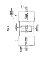
- Fig. 1 is a block diagram schematically illustrating a power conversion system and its input/output circuit according to the first embodiment of the present invention.
- a power conversion system 10 includes an AC power source 1 such as magnetic field AC generator and commercial power source, a first power converter 2 for converting first AC power supplied from the AC power source 1 into DC power, plural condensers 3 for smoothing DC voltage outputted from the first power converter 2, a second power converter 4 for converting the DC power outputted from the first power converter 2 into second AC power and a load 5 such as motor supplied with the second AC power outputted from the second power converter 4.
- parasitic inductance 6 is produced by connection routes between inner electrodes of the condensers 3 and external parallel wiring routes thereof.
- the plural condensers 3 (for example, ceramic condensers) having capacitance of temperature dependence (refer to Fig. 3 ) and the parasitic inductance 6 exist between the first and second power converters 2 and 4.
- a parallel resonance circuit is formed by the condensers 3 and parasitic inductance 6.
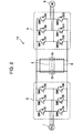
- Fig. 2 is a circuit diagram schematically illustrating the power conversion system and its input/output circuit according to the first embodiment of the present invention.
- the first power converter 2 is realized by a three-phase rectifier circuit, for example.
- the first power converter 2 includes switching elements SW1 to SW6 and backflow preventing rectifier elements D1 to D6 for the switching elements SW1 to SW6.
- the switching elements SW1 to SW6 are made of semiconductor switching elements such as, for example, IGBT (Insulated Gate Bipolar Transistor), MOSFET (Metal Oxide Semiconductor Field Effect Transistor) and GTO (Gate Turn Off Thyristor).
- the backflow preventing rectifier elements D1 to D6 are diodes, for example.
- the connection method of the switching elements SW1 to SW6 and the backflow preventing rectifier elements D1 to D6 is a general connection method of a rectifier circuit and description thereof is omitted.
- a gate signal (not shown) for controlling a conduction amount of the switching elements SW1 to SW6 is inputted externally so as to maintain an output-side voltage of the first power converter 2 to be a fixed value.
- the plural condensers 3 are provided to smooth DC voltage outputted from the first power converter 2 and are connected in parallel to the output side of the first power converter 2.
- the plural condensers 3 are composed of condensers C1 to Cn (n is an integer equal to or larger than 2) and plural condensers can be connected in parallel to one another to thereby increase its composite capacitance.
- the second power converter 4 is realized by a three-phase inverter, for example.
- the second power converter 4 includes switching elements SW7 to SW12 and backflow preventing rectifier elements D7 to D12 for the switching elements SW7 to SW12.
- the switching elements SW7 to SW12 are made of semiconductor switching elements such as, for example, IGBT (Insulated Gate Bipolar Transistor), MOSFET (Metal Oxide Semiconductor Field Effect Transistor) and GTO (Gate Turn Off Thyristor).
- the backflow preventing rectifier elements D7 to D12 are diodes, for example.
- the connection method of the switching elements SW7 to SW12 and the backflow preventing rectifier elements D7 to D12 is a general connection method of an inverter circuit and description thereof is omitted.
- Agate signal (not shown) for controlling a conduction amount of the switching elements SW7 to SW12 is inputted externally so as to supply AC power from the output side of the second power converter 4.
- AC power supplied from the AC power source 1 is converted into DC voltage by the first power converter 2.
- the DC voltage is smoothed by the plural condensers 3 to be supplied to the second power converter 4. Further, the DC voltage is converted into AC power by the second power converter 4 to be supplied to the load 5.
- the first power converter 2 shown in Fig. 2 constitutes a three-phase rectifier circuit and the second power converter 4 constitutes a three-phase inverter circuit, although if the AC power source 1 is, for example, a single-phase power source, the first power converter 2 of Fig. 1 is of single phase and is composed of two switching elements SW's (not shown). Furthermore, if the load 5 is a single-phase motor, the second power converter 4 of Fig. 1 is of single phase and is composed of two switching elements SW's (not shown).
- the circuit of the first power converter 2 can be configured properly in accordance with the number of phases of the AC power source 1 and the circuit of the second power converter 4 can be also configured properly in accordance with the number of phases of the load 5.
- Fig. 3 is a characteristic diagram showing the relation of temperature and capacitance of condensers applied to the first embodiment of the present invention.
- the horizontal axis represents temperature and the vertical axis represents capacitance.
- the capacitance of the condensers C1 to Cn shown in Fig. 2 has the temperature dependence as shown in Fig. 3 and is changed in accordance with temperature of the condensers. That is, the condensers has a so-called negative temperature dependence that the capacitance thereof is reduced with rise in temperature when a certain temperature is exceeded (for example, 0° C or more).
- the condensers having such a temperature dependence is, for example, ceramic condensers.
- the capacitance per unit volume of the ceramic condensers can be increased and accordingly the ceramic condensers are used by preference when plural condensers are connected in parallel to the DC input side of the power conversion system where large current flows.
- Figs. 4A and 4B are characteristic diagrams showing the relation between resonance frequency and carrier frequency applied to the embodiment.
- Fig. 4A shows the characteristic of carrier frequency, in which the horizontal axis represents frequency and the vertical axis represents input current (ripple current).
- Fig. 4B shows the characteristic of resonance frequency, in which the horizontal axis represents frequency and the vertical axis represents resonance response factor.
- fc represents carrier frequency
- 2fc represents double carrier frequency.
- the carrier frequency is a switching frequency or PWM (Pulse Width Modulation) frequency for driving the switching elements (SW1 to SW6) of the first power converter 2 or/and the switching elements (SW7 to SW12) of the second power converter 4.
- the input current of Fig. 4A represents current flowing through the plural condensers C1 to Cn.
- f1 of Fig. 4B represents resonance frequency at the lowest temperature within use temperature range and f2 represents resonance frequency at the highest temperature within the use temperature range.
- the resonance response factor is maximum when the carrier frequency is f1. That is, it is understood that f1 is the resonance frequency decided by parasitic inductance and all capacitance of the condensers C1 to Cn at the lowest temperature T1.
- the resonance response factor is maximum when the carrier frequency is f2. That is, it is understood that f2 is the resonance frequency decided by parasitic inductance and all capacitance of the condensers C1 to Cn at the highest temperature T2.
- the reason that the resonance characteristic of the condensers C1 to Cn is changed in accordance with use temperature is that the capacitance of the condensers C1 to Cn is changed in accordance with use temperature (refer to Fig. 3 ).
- the resonance frequency of the condensers C1 to Cn is made higher with rise in temperature and is coincident with the carrier frequency or an integral multiple of the carrier frequency, large current flows through the condensers C1 to Cn, so that it is apprehended that the condensers C1 to Cn break down.
- the resonance frequency f decided by inductance value L of parasitic inductance 6 formed among the plural condensers C1 to Cn connected in parallel to one another and all capacitance C of the condensers C1 to Cn within use temperature range is set to fall within the following range. That is, in the embodiment, the resonance frequency f falls within the range given by: mfc + ⁇ f ⁇ f ⁇ m + 1 ⁇ fc - ⁇ f where fc is a carrier frequency for driving at least one of switching elements SW1 to SW6 of the first power converter 2 and switching elements SW7 to SW12 of the second power converter 4 and m is an positive integer. This can be realized by adjusting the carrier frequency fc, all capacitance C of the condensers C1 to Cn and inductance value L of the parasitic inductance 6.
- fc is 600 Hz and ⁇ f is equal to or higher than 10 Hz and equal to or lower than 100 Hz, for example. Further, ⁇ f is selected so that the ripple current inputted in the condensers C1 to Cn is suppressed to be equal to or smaller than 200 Arms, for example, within the range of mfc+ ⁇ f ⁇ f ⁇ (m+1)fc- ⁇ f.
- the resonance characteristic of the condensers C1 to Cn is characteristic a and the resonance frequency thereof is f1. Further, at the highest temperature T2 within the use temperature range, the resonance characteristic of the condensers C1 to Cn is characteristic b and the resonance frequency thereof is f2. Consequently, the resonance frequency f decided by all capacitance C of the condensers C1 to Cn within the use temperature range is equal to or higher than f1 and equal to or lower than f2.
- the resonance frequency (f: f1 ⁇ f ⁇ f2) within the use temperature range shown in Fig. 4B falls within the range of fc+ ⁇ f ⁇ f ⁇ 2fc- ⁇ f as shown in Fig. 4A .
- fc is 600 Hz and ⁇ f is equal to or higher than 10 Hz and equal to or lower than 100 Hz, for example.
- the resonance frequency f may be set to fall within the range of 2fc+ ⁇ f ⁇ f ⁇ 3fc- ⁇ f or 3fc+ ⁇ f ⁇ f ⁇ 4fc- ⁇ f
- m is a positive integer and the resonance frequency f may be set to fall within the range of mfc+ ⁇ f ⁇ f ⁇ m+1)fc- ⁇ f This can be realized by adjusting the carrier frequency fc, all capacitance C of the condensers C1 to Cn and inductance value L of the parasitic inductance.
- the ripple current is produced or caused in synchronism with the frequency mfc equal to an integral multiple of the carrier frequency fc.
- the carrier frequency that is, the frequency of the ripple current is coincident with the resonance frequency of the circuit, large ripple current flows.
- the resonance frequency f(f1 ⁇ f ⁇ f2: refer to Fig. 4B ) within the use temperature range of the condensers is set to fall within the range of mfc+ ⁇ f ⁇ f ⁇ (m+1)fc- ⁇ f where m is a positive integer, so that the ripple current can be prevented from being increased.
- the carrier frequency and the resonance frequency decided by the composite capacitance of the condensers C1 to Cn within the use temperature range and the parasitic inductance 6 are not overlapped and accordingly it is not apprehended that large ripple current flows through the condensers. Consequently, temperature of the condensers can be converged to predetermined temperature level and thermal runaway caused by rise in temperature of the condensers C1 to Cn can be avoided. Accordingly, the reliability and safety of the power conversion system can be enhanced.
- the ceramic condensers when ceramic condensers are used as the plural condensers 3, the ceramic condensers have low ESR (Equivalent Series Resistance) and excellent thermal resistance and accordingly the merit that miniaturization is expedited can be utilized. Therefore, there can be provided the power conversion system capable of avoiding thermal runaway and having excellent reliability.
- ESR Equivalent Series Resistance
- the resonance frequency f within the use voltage range is set to fall within the range of mfc+ ⁇ f ⁇ f ⁇ (m+1)fc- ⁇ f where fc is carrier frequency and m is a positive integer, so that the ripple current can be reduced.
- Fig. 5 is a circuit diagram schematically illustrating a power conversion system and its input/output circuit according to the second embodiment of the present invention.
- the configuration of the power conversion system and its input/output circuit shown in Fig. 5 is the same as that of the power conversion system and its input/output circuit shown in Fig. 1 . Accordingly, description of constituent elements of the circuit thereof is omitted.
- Fig. 6 is a characteristic diagram showing the relation of DC voltage impressed to the condensers and capacitance thereof applied to the second embodiment of the present invention.
- the horizontal axis represents DC voltage and the vertical axis represents capacitance. That is, in the embodiment, the capacitance of the condensers C1 to Cn has the DC voltage dependence and as the DC voltage 11 (refer to Fig. 5 ) biased to the condensers C1 to Cn is made higher, the capacitance of the condensers is reduced.
- the relation of carrier frequency and input current is as shown in Fig. 4A and the relation of resonance frequency and resonance response factor is as shown in Fig. 4B . That is, in the power conversion system 10 of the embodiment, the resonance frequency f (refer to Fig.4B ) decided by inductance value L of the parasitic inductance 6 formed among the plural condensers 3 connected in parallel to one another and all capacitance C of the condensers 3 within the change range of the DC voltage 11 biased to the condensers 3 is set to fall within the following range. That is, in the embodiment, the resonance frequency f is set to fall within the range of mfc+ ⁇ f ⁇ f ⁇ (m+1)fc- ⁇ f where fc is carrier frequency and m is a positive integer.
- fc is 600 Hz and ⁇ f is equal to or higher than 10 Hz and equal to or lower than 100 Hz, for example. Further, ⁇ f is selected so that the ripple current inputted in the condensers C1 to Cn is suppressed to be equal to or smaller than 200 Arms, for example, within the range of mfc+ ⁇ f ⁇ f ⁇ (m+1)fc- ⁇ f
- the above setting can be realized by adjusting carrier frequency fc, all capacitance C of condensers C1 to Cn and inductance value L of parasitic inductance 6.
- the characteristic a represents the case where DC voltage 11 is lower and the characteristic b represents the case where DC voltage 11 is higher.
- the resonance characteristic of the condensers C1 to Cn is characteristic a and the resonance frequency thereof is f1 in the lowest voltage within the range of DC voltage 11 to be used. Further, the resonance characteristic of the condensers Cto Cn is characteristic b and the resonance frequency thereof is f2 in the highest voltage within the range of DC voltage 11 to be used. Consequently, the resonance frequency f decided by all capacitance C of the condensers C1 to Cn within the use range of DC voltage 11 is equal to or higher than f1 and equal to or lower than f2. Further, the reason that the resonance characteristic of the condensers C1 to Cn is changed in accordance with DC voltage 11 is that the capacitance of the condensers C1 to Cn is changed in accordance with DC voltage 11 as in Fig. 6 .
- the resonance frequency f decided by inductance value L of the parasitic inductance 6 formed among the plural condensers C1 to Cn connected in parallel to one another and all capacitance C of the condensers C1 to Cn within change range of DC voltage 11 impressed to the condensers C1 to Cn is set to fall within the following range. That is, as shown in Fig. 4A , the resonance frequency f is set to fall within the range of fC+ ⁇ f ⁇ f ⁇ 2fc- ⁇ f
- fc 600 Hz and ⁇ f is equal to or higher than 10 Hz and equal to or lower than 100 Hz, for example.
- the ripple current can be prevented from being increased and the reliability of the power converter 10 can be enhanced.
- the resonance frequency may be set to fall within the range of mfc+ ⁇ f ⁇ f ⁇ (m+1)fc- ⁇ f where m is a positive integer. Further, this can be realized by adjusting carrier frequency fc, all capacitance C of condensers C1 to Cn and inductance value L of parasitic inductance 6.
- the ceramic condensers when ceramic condensers are used as the condensers C1 to Cn, the ceramic condensers have low ESR and excellent thermal resistance and accordingly the merit that miniaturization is expedited can be utilized. Therefore, there can be provided the power conversion system capable of avoiding thermal runaway and having excellent reliability.
- thermal runaway of the condensers C1 to Cn can be suppressed as follows. That is, the resonance frequency f is set to fall within the range of mfc+ ⁇ f ⁇ f ⁇ (m+1)fc- ⁇ f, so that there can be realized the high-reliable power conversion system which can suppress the ripple current of condensers and avoid the thermal runaway of the condensers.
- the condensers used in the power conversion system of the present invention is made of dielectric material having temperature dependence and DC voltage dependence in capacitance. Ceramic condensers are mentioned as an example suitable for the condensers realized by such dielectric material. Since the ceramic condensers have large capacitance per unit volume, a large number of small ceramic condensers can be connected in parallel to one another between DC bus (DC input wiring). The power system including the power conversion system of a large-capacity type can be made still smaller.
- ceramic condensers are made of ceramic that is inorganic material, the ceramic condensers have excellent thermal resistance and ESR thereof can be made smaller. With such characteristics, the reliability of the power conversion system for high voltage and large current can be enhanced and the power system including the power conversion system can be made still smaller.
- the ripple current of condensers which are essential constituent elements in the power conversion system of AC-DC-AC conversion type can be made smaller so as to suppress rise in temperature of the condensers and the condensers can be made smaller. Accordingly, the power conversion system of the present invention can be utilized in large-power type power conversion system effectively.
Landscapes
- Engineering & Computer Science (AREA)
- Power Engineering (AREA)
- Inverter Devices (AREA)
- Power Conversion In General (AREA)
Applications Claiming Priority (1)
| Application Number | Priority Date | Filing Date | Title |
|---|---|---|---|
| JP2011084296A JP2012222892A (ja) | 2011-04-06 | 2011-04-06 | 電力変換装置 |
Publications (2)
| Publication Number | Publication Date |
|---|---|
| EP2509207A2 true EP2509207A2 (fr) | 2012-10-10 |
| EP2509207A3 EP2509207A3 (fr) | 2015-09-16 |
Family
ID=46000646
Family Applications (1)
| Application Number | Title | Priority Date | Filing Date |
|---|---|---|---|
| EP12002421.1A Withdrawn EP2509207A3 (fr) | 2011-04-06 | 2012-04-03 | Système de conversion d'alimentation |
Country Status (2)
| Country | Link |
|---|---|
| EP (1) | EP2509207A3 (fr) |
| JP (1) | JP2012222892A (fr) |
Cited By (1)
| Publication number | Priority date | Publication date | Assignee | Title |
|---|---|---|---|---|
| AT521100A1 (de) * | 2018-04-13 | 2019-10-15 | Ceracap Engel Kg | Wechselrichter mit Zwischenkreis |
Families Citing this family (7)
| Publication number | Priority date | Publication date | Assignee | Title |
|---|---|---|---|---|
| JP2015080370A (ja) * | 2013-10-18 | 2015-04-23 | ダイキン工業株式会社 | 電力変換装置 |
| JP6187197B2 (ja) * | 2013-11-29 | 2017-08-30 | ダイキン工業株式会社 | 電力変換装置 |
| JP6279158B2 (ja) * | 2015-07-24 | 2018-02-14 | 三菱電機株式会社 | 電力変換装置 |
| JP2017143647A (ja) * | 2016-02-10 | 2017-08-17 | 株式会社日立製作所 | 電力変換機装置 |
| JP7327036B2 (ja) * | 2019-09-20 | 2023-08-16 | 株式会社デンソー | 車両用の電力変換装置 |
| WO2024024023A1 (fr) | 2022-07-28 | 2024-02-01 | 東芝三菱電機産業システム株式会社 | Dispositif d'alimentation électrique |
| JP7531679B1 (ja) * | 2023-11-09 | 2024-08-09 | 日立ジョンソンコントロールズ空調株式会社 | 制御装置および空気調和装置 |
Citations (1)
| Publication number | Priority date | Publication date | Assignee | Title |
|---|---|---|---|---|
| JP2009060691A (ja) | 2007-08-30 | 2009-03-19 | Murata Mfg Co Ltd | インバータ装置及びその設計方法 |
Family Cites Families (9)
| Publication number | Priority date | Publication date | Assignee | Title |
|---|---|---|---|---|
| US3022A (en) * | 1843-03-30 | Machine for bending stibrups for paddle-wheels of steam and other | ||
| US9001A (en) * | 1852-06-08 | Keflector-lamp | ||
| US10022A (en) * | 1853-09-13 | Lard-lamp | ||
| JPH1118435A (ja) * | 1997-06-18 | 1999-01-22 | Mitsubishi Electric Corp | 直流リンク部の共振を抑制した高力率インバータ装置 |
| JP3637741B2 (ja) * | 1997-09-16 | 2005-04-13 | 富士電機システムズ株式会社 | 電力変換装置 |
| JP2003333859A (ja) * | 2002-05-14 | 2003-11-21 | Mitsubishi Electric Corp | 電力変換装置における平滑コンデンサ放電システム |
| JP5338154B2 (ja) * | 2007-07-06 | 2013-11-13 | 日産自動車株式会社 | 電力変換装置 |
| JP2009095202A (ja) * | 2007-10-12 | 2009-04-30 | Daikin Ind Ltd | インバータ |
| AT12748U1 (de) * | 2009-09-08 | 2012-10-15 | Siemens Ag | Frequenzumrichteranordnung |
-
2011
- 2011-04-06 JP JP2011084296A patent/JP2012222892A/ja active Pending
-
2012
- 2012-04-03 EP EP12002421.1A patent/EP2509207A3/fr not_active Withdrawn
Patent Citations (1)
| Publication number | Priority date | Publication date | Assignee | Title |
|---|---|---|---|---|
| JP2009060691A (ja) | 2007-08-30 | 2009-03-19 | Murata Mfg Co Ltd | インバータ装置及びその設計方法 |
Cited By (2)
| Publication number | Priority date | Publication date | Assignee | Title |
|---|---|---|---|---|
| AT521100A1 (de) * | 2018-04-13 | 2019-10-15 | Ceracap Engel Kg | Wechselrichter mit Zwischenkreis |
| WO2019195867A1 (fr) * | 2018-04-13 | 2019-10-17 | Ceracap Engel Kg | Onduleur à circuit intermédiaire |
Also Published As
| Publication number | Publication date |
|---|---|
| JP2012222892A (ja) | 2012-11-12 |
| EP2509207A3 (fr) | 2015-09-16 |
Similar Documents
| Publication | Publication Date | Title |
|---|---|---|
| EP2509207A2 (fr) | Système de conversion d'alimentation | |
| US8279639B2 (en) | Direct AC power converting apparatus | |
| EP2104218B1 (fr) | Convertisseur avec une multitude des convertisseurs alternatifs indirects à liaison en tension | |
| CN105191100B (zh) | 双向dc/dc转换器 | |
| US10411588B2 (en) | Power converter with trench and planar transistors to improve efficiency | |
| JP5369922B2 (ja) | 3レベル電力変換装置 | |
| US11267351B2 (en) | Power conversion device | |
| EP2590212A1 (fr) | Module semi-conducteur de puissance, transformateur électrique, et wagon | |
| US20130038140A1 (en) | Switching circuit | |
| JP2014533487A (ja) | Hブリッジに基づく電力変換器 | |
| CN105075102A (zh) | 电力转换装置、具备其的电动机驱动装置、具备其的鼓风机、压缩机、以及具备这些的空调机、冰箱和制冷机 | |
| US10027234B2 (en) | Power conversion device for performing power conversion between DC and DC by controlling switching of a semiconductor switching element | |
| EP3029821B1 (fr) | Dispositif semi-conducteur et dispositif de conversion d'énergie | |
| JP2014068428A (ja) | 電力変換装置 | |
| JPWO2015056491A1 (ja) | 電力変換装置及び電力変換方法 | |
| US11165359B2 (en) | Power conversion system configured to perform power conversion between direct current and three-phase alternating current | |
| JP2017143647A (ja) | 電力変換機装置 | |
| JP5930978B2 (ja) | Dc/dcコンバータ | |
| US8064232B2 (en) | Power conversion device and power conversion system | |
| JP5443289B2 (ja) | 電力変換装置 | |
| JP6513564B2 (ja) | 共振回避可能なインバータ装置 | |
| US20190245427A1 (en) | System and method for the conversion of dc electric power into three-phase ac electric power, with filtering means | |
| US20200321851A1 (en) | Main conversion circuit, power conversion device, and moving body | |
| CN112236930B (zh) | 电力转换装置 | |
| JP2018528753A (ja) | スイッチング過電圧を制限するために構成されるパワーコンバータ |
Legal Events
| Date | Code | Title | Description |
|---|---|---|---|
| PUAI | Public reference made under article 153(3) epc to a published international application that has entered the european phase |
Free format text: ORIGINAL CODE: 0009012 |
|
| 17P | Request for examination filed |
Effective date: 20120801 |
|
| AK | Designated contracting states |
Kind code of ref document: A2 Designated state(s): AL AT BE BG CH CY CZ DE DK EE ES FI FR GB GR HR HU IE IS IT LI LT LU LV MC MK MT NL NO PL PT RO RS SE SI SK SM TR |
|
| AX | Request for extension of the european patent |
Extension state: BA ME |
|
| RBV | Designated contracting states (corrected) |
Designated state(s): AL AT BE BG CH CY CZ DE DK EE ES FI FR GB GR HR HU IE IS IT LI LT LU LV MC MK MT NL NO PL PT RO RS SE SI SK SM TR |
|
| PUAL | Search report despatched |
Free format text: ORIGINAL CODE: 0009013 |
|
| STAA | Information on the status of an ep patent application or granted ep patent |
Free format text: STATUS: THE APPLICATION HAS BEEN WITHDRAWN |
|
| AK | Designated contracting states |
Kind code of ref document: A3 Designated state(s): AL AT BE BG CH CY CZ DE DK EE ES FI FR GB GR HR HU IE IS IT LI LT LU LV MC MK MT NL NO PL PT RO RS SE SI SK SM TR |
|
| AX | Request for extension of the european patent |
Extension state: BA ME |
|
| RIC1 | Information provided on ipc code assigned before grant |
Ipc: H02M 1/14 20060101ALI20150810BHEP Ipc: H02M 5/458 20060101AFI20150810BHEP |
|
| 18W | Application withdrawn |
Effective date: 20150903 |