EP2515444B1 - Transmetteur RF et procédé associé - Google Patents
Transmetteur RF et procédé associé Download PDFInfo
- Publication number
- EP2515444B1 EP2515444B1 EP12002263.7A EP12002263A EP2515444B1 EP 2515444 B1 EP2515444 B1 EP 2515444B1 EP 12002263 A EP12002263 A EP 12002263A EP 2515444 B1 EP2515444 B1 EP 2515444B1
- Authority
- EP
- European Patent Office
- Prior art keywords
- digital
- signal
- phase
- quadrature
- distortion
- Prior art date
- Legal status (The legal status is an assumption and is not a legal conclusion. Google has not performed a legal analysis and makes no representation as to the accuracy of the status listed.)
- Active
Links
Images


Classifications
-
- H—ELECTRICITY
- H04—ELECTRIC COMMUNICATION TECHNIQUE
- H04B—TRANSMISSION
- H04B1/00—Details of transmission systems, not covered by a single one of groups H04B3/00 - H04B13/00; Details of transmission systems not characterised by the medium used for transmission
- H04B1/02—Transmitters
- H04B1/04—Circuits
- H04B1/0475—Circuits with means for limiting noise, interference or distortion
-
- H—ELECTRICITY
- H03—ELECTRONIC CIRCUITRY
- H03F—AMPLIFIERS
- H03F1/00—Details of amplifiers with only discharge tubes, only semiconductor devices or only unspecified devices as amplifying elements
- H03F1/32—Modifications of amplifiers to reduce non-linear distortion
- H03F1/3241—Modifications of amplifiers to reduce non-linear distortion using predistortion circuits
-
- H—ELECTRICITY
- H04—ELECTRIC COMMUNICATION TECHNIQUE
- H04L—TRANSMISSION OF DIGITAL INFORMATION, e.g. TELEGRAPHIC COMMUNICATION
- H04L27/00—Modulated-carrier systems
- H04L27/32—Carrier systems characterised by combinations of two or more of the types covered by groups H04L27/02, H04L27/10, H04L27/18 or H04L27/26
- H04L27/34—Amplitude- and phase-modulated carrier systems, e.g. quadrature-amplitude modulated carrier systems
- H04L27/36—Modulator circuits; Transmitter circuits
- H04L27/366—Arrangements for compensating undesirable properties of the transmission path between the modulator and the demodulator
- H04L27/367—Arrangements for compensating undesirable properties of the transmission path between the modulator and the demodulator using predistortion
- H04L27/368—Arrangements for compensating undesirable properties of the transmission path between the modulator and the demodulator using predistortion adaptive predistortion
-
- H—ELECTRICITY
- H04—ELECTRIC COMMUNICATION TECHNIQUE
- H04B—TRANSMISSION
- H04B1/00—Details of transmission systems, not covered by a single one of groups H04B3/00 - H04B13/00; Details of transmission systems not characterised by the medium used for transmission
- H04B1/02—Transmitters
- H04B1/04—Circuits
- H04B1/0483—Transmitters with multiple parallel paths
-
- H—ELECTRICITY
- H04—ELECTRIC COMMUNICATION TECHNIQUE
- H04B—TRANSMISSION
- H04B1/00—Details of transmission systems, not covered by a single one of groups H04B3/00 - H04B13/00; Details of transmission systems not characterised by the medium used for transmission
- H04B1/02—Transmitters
- H04B1/04—Circuits
- H04B2001/0408—Circuits with power amplifiers
- H04B2001/0425—Circuits with power amplifiers with linearisation using predistortion
Definitions
- the present invention relates to a radio frequency transmitter and a method therefor according to the pre-characterizing clauses of claims 1 and 9.
- CMOS Complementary Metal-Oxide Semiconductor
- RF radio frequency
- a large number of conventional RF transmitters use linear power amplifiers (PAs).
- PAs linear power amplifiers
- JP 2007 049 621 A discloses a predistortion amplifier for use with such a linear power amplifier in order to compensate a non-linearity thereof under temperature change. Accordingly, the power efficiency of such conventional RF transmitters is usually very low, due to the low efficiency of the linear PAs used therein.
- Switch-mode PAs have very high efficiency in comparison, which make such switch-mode PAs an attractive alternative to conventional linear PAs within RF transmitters.
- an RF transmitter that is able to utilize switch-mode PAs through the assistance of digital processing algorithms in order to reduce a PA's size and improve a PA's power efficiency is highly desirable.
- switch-mode PAs normally exhibit a highly non-linear input-output relationship.
- noise shaping techniques are often required.
- Digital polar transmitters are a type of known transmitter design that utilizes switch-mode PAs, whilst also taking advantage of CMOS process technology. Accordingly, such digital polar transmitters are able to achieve high power efficiency, whilst requiring only a small silicon area.
- CMOS process technology complementary metal-oxide-semiconductor
- a problem with these known transmitter designs is that, due to the inherent bandwidth expansion characteristics of the AM (amplitude modulation) and PM (phase modulation) signals in a polar architecture, they are only suitable for narrowband modulated signals.
- Hybrid polar transmitter designs take advantage of two dimensional (in-phase/quadrature) modulation to enable wideband phase modulation to achieved.
- a problem with such hybrid polar transmitters is that they suffer from both amplitude and phase quantization noise, thus requiring significant noise shaping.
- I/Q RF DACs combine the functionalities of a DAC and a mixer, with the output of the I/Q RF DAC being combined in the analogue (RF) domain.
- RF analogue
- US 2009/051426 A1 discloses a predistorter for a PA in a WCDMA transmitter having such a transmitter design.
- Another known (predominantly narrowband) RF transmitter design utilizes adaptive pre-distortion using a delta-sigma modulator for automatic inversion of power amplifier non-linearity.
- Such a design is relatively simple and allows for a use of low-precision DACs.
- this design still comprises a generally conventional architecture, and so PA efficiency is low.
- Document US2010105338 discloses a method for performing amplitude modulation/phase modulation predistortion to linearize digitally controlled transmission amplifier in a communication transceiver. It is anticipated that digitally-assisted/ digitally-intensive RF transmitters will become increasingly desirable.
- digital algorithms are limited by the availability of circuit speed; therefore finding simple and effective digital algorithms is crucial from an implementation perspective.
- published literature currently available there are sometimes discussions on digital algorithms that operate at very high clock frequencies, such as four times the carrier frequency. However, such clock frequencies are, in a practical CMOS and/or subscriber communication unit sense, not implementable.
- the present invention aims at providing an RF transmitter and method therefor to mitigate, alleviate or eliminate one or more of the above mentioned disadvantages singly or in any combination.
- a radio frequency (RF) transmitter comprising at least one digital signal processing module comprising at least one digital pre-distortion component arranged to receive at least one complex input signal comprising information to be transmitted over an RF interface, perform two-dimensional non-uniform mapping of the at least one received complex input signal to a first, in-phase digital pre-distortion control word and at least one further, quadrature digital pre-distortion control word, and to output the in-phase and quadrature digital pre-distortion control words.
- RF radio frequency
- the RF transmitter further comprises at least one power amplifier module comprising a first, in-phase, array of switch-mode power cells and at least one further, quadrature array of switch-mode power cells, wherein the first, in-phase and further quadrature control words are arranged to drive the at least one power amplifier module to output an analogue RF signal that represents the at least one complex input signal and wherein two-dimensional non-uniform mapping comprises a pre-distortion profile that is at least partly based on an input/output relationship for the at least one power amplifier module.
- the at least one power amplifier module is arranged to receive the in-phase and quadrature digital pre-distortion control words output by the at least one digital signal processing module, and to generate an analogue RF signal for transmission over an RF interface based at least partly on the in-phase and quadrature digital pre-distortion control words.
- the RF transmitter comprises a complex signal based architecture, i.e. an IQ based architecture, and as such is suitable for both narrowband and wideband modulation input signals.
- a digital polar architecture which is only suitable for narrowband modulated signals due to the inherent bandwidth expansion characteristics of the AM (amplitude modulation) and PM (phase modulation) input signals of a polar architecture.
- the RF transmitter also extends the digital domain through to the power amplifier module, thereby benefiting from the scalability and efficiency of digital components to a greater extent than conventional RF architectures. Furthermore, the RF transmitter takes advantage of the efficiency of switch-mode power cells. Further still, the two-dimensional non-uniform mapping of the input signals provides pre-distortion of the input signals, thereby enabling the non-linearity of the switch-mode power cells to be compensated for, also within the digital domain.
- the at least one digital signal processing module may comprise at least one digital pre-distortion component arranged to receive the at least one complex input signal, perform two-dimensional non-uniform mapping of the at least one received complex input signal to a first, in-phase digital pre-distortion control word and at least one further, quadrature digital pre-distortion control word, and to output the in-phase and quadrature digital pre-distortion control words.
- at least one digital pre-distortion component arranged to receive the at least one complex input signal, perform two-dimensional non-uniform mapping of the at least one received complex input signal to a first, in-phase digital pre-distortion control word and at least one further, quadrature digital pre-distortion control word, and to output the in-phase and quadrature digital pre-distortion control words.
- the at least one digital pre-distortion component may be arranged to receive the at least one complex input signal, identify a closest matching predefined vector for the received at least one complex input signal within a two-dimensional pre-distortion profile, and map the identified predefined vector to a set of digital control words to be output.
- the two-dimensional pre-distortion profile may be at least partly based on an input/output relationship for the power amplifier module; in particular the two-dimensional pre-distortion profile may be at least partly based on an input/output relationship for the arrays of the switch-mode power cells of the power amplifier module.
- the at least one digital signal processing module may comprise at least one noise shaping component arranged to receive the at least one complex input signal and at least one feedback signal from the at least one digital pre-distortion component, apply noise shaping to the at least one complex input signal based at least partly on the at least one feedback signal, and output at least one noise shaped complex input signal.
- at least one noise shaping component arranged to receive the at least one complex input signal and at least one feedback signal from the at least one digital pre-distortion component, apply noise shaping to the at least one complex input signal based at least partly on the at least one feedback signal, and output at least one noise shaped complex input signal.
- the at least one digital pre-distortion component may be arranged to receive the at least one noise shaped complex input signal, perform two-dimensional non-uniform mapping of the at least one noise shaped complex input signal to a first, in-phase digital pre-distortion control word and at least one further, quadrature digital pre-distortion control word, and to output the in-phase and quadrature digital pre-distortion control words.
- the at least one noise shaping component and the at least one digital pre-distortion component may form at least part of a delta sigma modulator.
- the at least one digital signal processing module may comprise an up-sampling component arranged to perform up-sampling of the received at least one complex input signal to increase a sample rate of the received at least one complex input signal to an input data rate of the at least one power amplifier module.
- the first array of switch-mode power cells may be arranged to receive at least a part of the first, in-phase digital pre-distortion control word and to generate a first, in-phase component of the analogue RF signal based at least partly on the first, in-phase digital pre-distortion control word, and the at least one further, quadrature, array of switch-mode power cells may be arranged to receive the at least one further, quadrature digital pre-distortion control word and to generate at least one further quadrature, component of the analogue RF signal based at least partly on the at least one further, quadrature digital pre-distortion control word.
- the first, in-phase, array of switch-mode power cells and the at least one further, quadrature, array of switch-mode power cells may be further arranged to receive respective carrier frequency signals, and to generate the respective first, in-phase, component and at least one further, quadrature, component of the analogue RF signal further based at least partly on the received carrier frequency signals.
- the power amplifier module may comprises a first, in-phase, phase selector arranged to receive a carrier frequency signal and a first, in-phase, sign signal, and to output a first, in-phase, carrier frequency signal for the first, in-phase, array of switch-mode power cells; and at least one further, quadrature, phase selector arranged to receive a carrier frequency signal and at least one further, quadrature, sign signal, and to output at least one further, quadrature, carrier frequency signal for the at least one further, quadrature, array of switch-mode power cells.
- the at least one power amplifier module may comprise a magnitude and sign generator module arranged to receive the digital pre-distortion control words output by the at least one digital signal processing module; and generate from each digital pre-distortion control word a magnitude control word comprising a magnitude component of the respective digital control word, and a sign signal comprising a sign component of the respective digital control word.
- each array of switch-mode power cells may comprise a plurality of inverse Class D structure switch-mode power cells
- an integrated circuit device comprising a signal processing module comprising at least one digital pre-distortion component substantially according to the first aspect of the invention.
- a wireless communication unit comprising a radio frequency transmitter according to the first aspect of the invention.
- a method of generating a radio frequency signal for transmission over a radio frequency (RF) interface comprises receiving at least one complex (in-phase/quadrature) input signal comprising information to be transmitted over the RF interface; performing two-dimensional non-uniform mapping of the at least one received complex input signal to a first, in-phase, digital pre-distortion control word and at least one further, quadrature, digital pre-distortion control word; providing the in-phase and quadrature digital pre-distortion control words to at least one power amplifier module comprising a first, in-phase, array of switch-mode power cells and at least one further quadrature, array of switch-mode power cells, wherein the first, in-phase and further quadrature control words are arranged to drive the at least one power amplifier module to output an analogue RF signal that represents the at least one complex input signal and wherein two-dimensional non-uniform mapping comprises a pre-distortion profile that is at least partly
- RF radio frequency
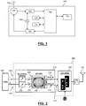
- the electronic device 100 in the context of the illustrated embodiment of the invention, is a wireless telecommunication handset.
- the electronic device 100 comprises an antenna 102 and contains a variety of well known radio frequency transceiver components or circuits operably coupled to the antenna 102.
- the antenna 102 is operably coupled to a duplex filter or antenna switch 104 that provides isolation between a receiver chain 106 and a transmitter chain 1 07.
- the receiver chain 106 typically includes radio frequency receiver circuitry for providing reception, filtering and intermediate or base-band frequency conversion.
- the transmitter chain 107 typically includes radio frequency transmitter circuitry for providing modulation and power amplification.
- An oscillator 130 is arranged to provide oscillation signals needed by the receiver chain 106 and the transmitter chain 107.
- the electronic device 100 further comprises signal processing logic 108.
- An output from the signal processing logic 108 may be provided to a suitable user interface (UI) 110 comprising, for example, a display, keypad, microphone, speaker, etc.
- UI user interface
- the signal processing logic 108 may also be coupled to a memory element 116 that stores operating regimes, such as decoding/encoding functions and the like and may be realised in a variety of technologies, such as random access memory (RAM) (volatile), (non-volatile) read only memory (ROM), Flash memory or any combination of these or other memory technologies.
- a timer 118 is typically coupled to the signal processing logic 108 to control the timing of operations within the electronic device 100.
- the transmitter chain 107 of such a wireless telecommunication handset comprises transmitter circuitry arranged to receive an input signal, for example from, in the illustrated example, the signal processing logic 108; the input signal comprising information to be transmitted over an RF interface.
- the transmitter chain 107 is further arranged to output an RF signal comprising the information to be transmitted to, in the illustrated example, the antenna 102 via the antenna switch 104.
- the transmitter chain 107 is typically required to perform digital to analogue conversion, mixing, noise shaping and amplification of the input signal in order to generate the RF signal output thereby.
- the RF transmitter 200 of FIG. 2 comprises a digital signal processing module 210 arranged to receive one or more complex input signals comprising information to be transmitted over an RF interface, for example via antenna 102 of FIG. 1 .
- the digital signal processing module 210 is arranged to receive from a digital baseband (DBB) component, such as the signal processing logic 108 of FIG.
- DBB digital baseband
- an IQ (In-phase/Quadrature) input signal comprising a first (In-phase) signal component (i.e., I) 222 and a second (Quadrature) signal component (i.e., Q) 224.
- the digital signal processing module 210 is further arranged to perform mapping of the received complex input signal(s) 222, 224 to a first, in-phase, digital control word (IDPA_W) 212 and a second, quadrature, digital control word (QDPA_W) 214, and to output the in-phase and quadrature digital control words to power amplifier module, such as a two-dimensional digital power amplifier (2D-DPA) 230.
- the power amplifier module 230 comprises a first (in-phase) array of switch-mode power cells and, in the illustrated example, a second (quadrature) array of switch-mode power cells, as described in greater detail below with reference to FIG. 5 .
- the power amplifier module 230 is arranged to receive the digital control words output by the digital signal processing module 210, and to generate an analogue RF signal for transmission over an RF interface, for example via antenna 102, based at least partly on the received in-phase and quadrature digital control words.
- the RF transmitter 200 comprises a complex signal based architecture, for example an IQ based architecture, and as such is suitable for both narrowband and wideband modulation input signals.
- a complex signal based architecture for example an IQ based architecture
- IQ based architecture avoids the need for implementing complex algorithms, such as the CORDIC (Coordinate rotation digital computer) algorithm typically required for digital polar architectures.
- the RF transmitter 200 also extends the digital domain through to the power amplifier module 230, thereby benefiting from the scalability and efficiency of digital components to a greater extent than conventional RF architectures. Furthermore, the RF transmitter 200 illustrated in FIG. 2 takes advantage of the efficiency of switch-mode power cells.
- Switch-mode power cells typically exhibit a highly non-linear input-output relationship, in particular when output power is high. Accordingly, the digital signal processing module 210 is arranged to perform two-dimensional non-uniform mapping of the input signals 222, 224 (as described in greater detail below) to the digital control words 212, 214. In this manner, the two-dimensional non-uniform mapping of the input signals 222, 224 provides pre-distortion of the input signals 222, 224, thereby enabling the non-linearity of the switch-mode power cells to be compensated for, also within the digital domain.
- digital pre-distortion is required to be performed with a sampling rate that is greater than that of the received complex input signal (for example in the region of three times that of the input signal) in order to preserve a certain spectrum at the output of the two-dimensional digital pre-distortion (2D DPD) component 250.
- the digital signal processing module 210 of the RF transmitter 200 of FIG. 2 comprises an up-sampling & filtering component 240 arranged to perform up-sampling of the received complex input signal 222, 224 to increase the sample rate thereof to, for example, an input data rate of the power amplifier module 230.
- the input to the power amplifier module 230 may comprise a 'sample and hold' operation.
- so-called DAC images may be seen at the output of the power amplifier module 230 that are spaced from each other by the sampling frequency at the input of the power amplifier module 230. Accordingly, up-sampling of the input signal components 222, 224 may enable the spacing of such images to be increased.
- the digital signal processing module 210 of the RF transmitter 200 of FIG. 2 further comprises a digital pre-distortion component 250 arranged to perform the non-uniform mapping of the up-sampled input signals (i.e., I_u and Q_u) 242, 244 to the digital control words 212, 214.
- the digital control words 21 2, 214 are output to one or more output ports 231 for coupling to one or more input ports of a power amplifier module 230.
- FIG. 2 is shown as comprising, say, a discrete integrated circuit comprising, at least, the signal processing module 210 that can be operably coupled to a distinct power amplifier module 230, it is envisaged in other examples that an integrated circuit may comprise the functionality of at least both the signal processing module 210 and the power amplifier module 230.
- the digital signal processing module 210 may comprise a digital pre-distortion component 250 arranged to receive the up-sampled in-phase and quadrature components 242, 244 of the complex input signal, identify a closest matching predefined vector for the received complex input signal within a pre-distortion profile 350, and map the identified predefined vector to a set of digital control words to be output.
- the digital pre-distortion component 250 of the illustrated example is arranged to perform quantization and to simultaneously apply pre-distortion to the received up-sampled in-phase and quadrature components 242, 244 of the complex input signal using the pre-distortion profile 350.
- the pre-distortion profile 350 may be at least partly based on an input/output relationship for the power amplifier module 230, and in particular the pre-distortion profile 350 may be at least partly based on an input/output relationship for the switch-mode power cell arrays of the power amplifier module 230. In this manner, pre-distortion may be applied to the up-sampled input signals 242, 244 that compensates for power amplifier module characteristics (and in particular the non-linear switch-mode power cell characteristics).
- the digital pre-distortion component 250 is implemented within a feed-forward path (as opposed to a feedback path). In this manner, the digital pre-distortion component 250 is able to directly compensate for the non-linearity of the power amplifier module 230 for each input sample. Such sample-by-sample digital pre-distortion is more accurate and responsive than digital pre-distortion that is averaged across multiple input samples within a feedback path.
- the digital pre-distortion module component 250 and power amplifier module 230 may be provided with a common clock signal 310.
- the digital signal processing module 210 is arranged to receive the complex (IQ) input signal 222, 224, up-sample and non-uniformly map the received signal to digital control words 212, 214 such that pre-distortion is applied to compensate for the non-linear characteristics of the power amplifier module 230, and to output digital control words 212, 214 to the power amplifier module 230, wherein the digital control words 212, 214 are arranged to drive the power amplifier module 230 to output an analogue RF signal that represents the up-sampled complex (IQ) input signal 242, 244.
- IQ complex
- a pre-distortion profile 350 used for mapping the up-sampled input signal components 242, 244 to the digital control words 212, 214 may be at least partly based on the input/output relationship for the switch-mode power cell arrays of the power amplifier module 230 to adaptively compensate for the non-linearities of the switch-mode power cell arrays.
- the digital signal processing module 210 of the illustrated example provides two dimensional (IQ) digital pre-distortion functionality within a feed-forward path of the RF transmitter 200.
- the RF transmitter 400 comprising an alternative example of a digital signal processing module 410 arranged to received from a digital baseband component, such as the signal processing logic 108 of FIG. 1 , a complex (IQ) input signal 222, 224, perform mapping of the received complex input signal 222, 224 to digital control words 212, 214, and to output the digital control words 21 2, 214 to the power amplifier module 230.
- the digital signal processing module 410 comprises an up-sampling component 240 arranged to perform up-sampling of the received complex input signal 222, 224 to increase the sample rate thereof to, for example, an input data rate of the power amplifier module 230.
- the digital processing module 410 further comprises a digital pre-distortion component 250 arranged to perform non-uniform mapping of the up-sampled input signals 242, 244 to the digital control words 21 2, 214.
- the digital signal processing module 410 of FIG. 4 further comprises a noise shaping component/noise shaper 420.
- the noise shaping component 420 is arranged to receive the complex input signal, which for the illustrated example comprises the first (In-phase) and second (Quadrature) up-sampled signal components 242, 244, and one or more feedback signals 422, 424 from the digital pre-distortion component 250.
- the noise shaping component 420 is further arranged to apply noise shaping to the received complex input signal components 242, 244 based at least partly on the received feedback signals 422, 424, and to output to the digital pre-distortion component 250 the noise shaped input signal components 442, 444.
- the digital pre-distortion component 250 is arranged to perform non-uniform mapping of the up-sampled noise shaped input signal components 442, 444 to the digital control words 212, 214.
- noise shaping of the complex input signal 222, 224 may be performed within the digital domain, and within the feed-forward path, prior to the non-uniform mapping to the digital control words 212, 214, enabling noise shaping to be maintained at the far-out region from the carrier, thus improving the spectrum at the desired far-out frequency band.
- noise shaping may be implemented through a configurable and/or programmable noise transfer function.
- the RF transmitter may be configured and/or programmed to perform required noise shaping to meet stringent co-existence requirements of a plurality of different wireless standards.
- the noise shaping component 420 and digital pre-distortion component 250 may be arranged to form a delta-sigma modulator, as illustrated at 450.
- the delta-sigma modulator 450 is arranged to receive the up-sampled complex (IQ) input signals 242, 244, and non-uniformly map the received signals to digital control words 212, 214 such that noise shaping and pre-distortion is applied to compensate for the non-linear characteristics of the power amplifier module 230, and to output digital control words 212, 214 to the power amplifier module 230, wherein the digital control words 212,214 are arranged to drive the power amplifier module 230 to output an analogue RF signal that represents the up-sampled complex (IQ) input signal 242, 244.
- IQ complex
- the aforementioned pre-distortion profile 350 used for mapping the up-sampled and noise shaped input signal components 242, 244 to the digital control words 212, 214 may be at least partly based on the input/output relationship for the switch-mode power cell arrays of the power amplifier module 230 to adaptively compensate for the non-linearities of the switch-mode power cell arrays.
- the implementation of quantization and two-dimensional digital pre-distortion within the delta-sigma modulator 450 in this manner may result in any quantization noise being relative to the pre-distortion profile, thereby enabling noise shaping to be achieved.
- the noise shaping effect would be at least partly washed-out by the non-linearity of the power amplifier module 230, and thus such noise shaping would not be seen at the output of the power amplifier module 230. This is due to the digital pre-distortion only being able to mitigate non-linearity at frequencies close to the signal; whereas noise shaping is often required at frequencies far away from the signal band.
- the power amplifier module 230 is arranged to receive the digital control words 212, 214 output by the digital signal processing module 210, and to output an analogue RF signal 530 for transmission over an RF interface, for example via the antenna 102 of FIG. 1 , based at least partly on the received digital control words 212, 214.
- the power amplifier module 230 comprises a first array of switch-mode power cells (I-PA) 510 and, in the illustrated example, a second array of switch-mode power cells (Q-PA) 520.
- the first array of switch-mode power cells 510 is arranged to receive at least a part of the first (e.g.
- the second array of switch-mode power cells 520 is arranged to receive at least a part of the second (e.g. quadrature) digital control word 214 and to generate a second (e.g. quadrature) component 534 of the analogue RF signal 530 based at least partly on the received digital control word 214.
- the separate components 532, 534 are subsequently combined to generate the complex analogue RF signal 530.
- a power amplifier module 230 is achieved that is capable of being digitally controlled to generate a multi-dimensional (e.g. IQ) amplified signal.
- each of the arrays of switch-mode power cells 510, 520 may be arranged to receive at least a part of the respective digital control word 212, 214 comprising, say, N control bits. Furthermore, each of the arrays of switch-mode power cells 510, 520 may comprise N switch-mode power cells; each of the switch-mode power cells being arranged to receive a respective control bit of the respective digital control word 212, 214.
- An example of such a switch-mode power cell is illustrated at 570, which for the illustrated example comprises a high efficiency inverse Class D structure.
- Each of the switch-mode power cells 570 is arranged to receive a respective control bit, illustrated at 575, and to selectively output a current signal (I out +/I out -) 574 based on the value of the received control bit 575.
- the outputs of the switch-mode power cells 570 within each array 510, 520 are operably coupled together such that the individual power cell output current signals (I out +/I out -) 574 are combined to provide the respective component 532, 534 of the analogue RF signal 530.
- the output current signal (I out +/I out -) 574 for the individual switch-mode power cells 570 within each array 510, 520 may be weighted in accordance with the significance of their respective control bits. In this manner, the combined output current signal of each array 510, 520 may be representative of the value of the digital control word received thereby.
- the power amplifier module 230 illustrated in FIG. 5 enables digital to analogue conversion functionality to be combined with power amplifier functionality, thereby simplifying the RF transmitter design. Furthermore, the provision of separate switch-mode power cell arrays 510, 520 to support the separate I and Q components of the complex IQ input signal enables the power amplifier module 230 to be suitable for both narrowband and wideband modulation input signals.
- the switch-mode power cell arrays 510, 520 of the power amplifier module 230 illustrated in FIG. 5 are further arranged to receive respective carrier frequency signals 540, 545, and to generate the respective components 532, 534 of the analogue RF signal 530 further based at least partly on the received carrier frequency signals 540, 545.
- the respective carrier frequency signal 540, 545 may be provided to each individual switch-mode power cell, such as illustrated at 540 within the illustrated power cell 570.
- the power amplifier module 230 illustrated in FIG. 5 enables mixing functionality to also be combined with the power amplifier functionality and digital to analogue conversion functionality.
- the power amplifier module 230 comprises a first (in-phase) phase selector 550 arranged to receive a first carrier frequency signal (LO_I) 552 and an in-phase sign signal 554, and to output an in-phase carrier frequency signal 540 for the first (in-phase) switch-mode power cell array 510 comprising a polarity based at least partly on the received in-phase sign signal 554.
- LO_I first carrier frequency signal
- LO_I carrier frequency signal
- the power amplifier module 230 comprises a first (in-phase) phase selector 550 arranged to receive a first carrier frequency signal (LO_I) 552 and an in-phase sign signal 554, and to output an in-phase carrier frequency signal 540 for the first (in-phase) switch-mode power cell array 510 comprising a polarity based at least partly on the received in-phase sign signal 554.
- the power amplifier module 230 further comprises, for the illustrated example, a second (quadrature) phase selector 555 arranged to receive a second carrier frequency signal (LO_Q) 557 and a quadrature sign signal 559, and to output a quadrature carrier frequency signal 545 for the second (quadrature) switch-mode power cell array 520 comprising a polarity based at least partly on the received quadrature sign signal 559.
- a second (quadrature) phase selector 555 arranged to receive a second carrier frequency signal (LO_Q) 557 and a quadrature sign signal 559, and to output a quadrature carrier frequency signal 545 for the second (quadrature) switch-mode power cell array 520 comprising a polarity based at least partly on the received quadrature sign signal 559.
- the power amplifier module 230 of the illustrated example further comprises a magnitude and sign generator module 560.
- the magnitude and sign generator module 560 is arranged to receive the digital control words 212, 214 output by the digital signal processing module 210, and from each of the digital control words 212, 214 generate a magnitude control word 512, 514, comprising a magnitude component of the respective digital control word 212, 214, and a sign signal 554, 559, comprising a sign component of the respective digital control word 212, 214.
- the magnitude control words 512, 514 are then provided to the respective switch-mode power cell arrays 510, 520, and the sign signals 554, 559 are provided to the respective phase selectors 550, 555. In this manner, the sign and magnitude of the in-phase and quadrature signal components may be separated to facilitate the use of switch-mode power cells.
- the digital domain extends through to the power amplifier module 230, there is no need for a linear pre-driver amplifier or baseband filter.
- the use of digitally controlled power cells enables the power consumption of the power amplifier module 230 to be scalable to substantially instantaneous RF output power.
- the output impedance of the power amplifier module 230 is a function of signal power level (i.e. compression). Accordingly, the effective load for each switch-mode power cell array 510, 520 will comprise a combination of the load present on the output signal 530 and the output impedance of the opposing switch-mode power cell array 510, 520.
- the effective load for the first (in-phase) power cell array 510 will comprise a combination of the load present on the output signal 530 and the output impedance of the second (quadrature) power cell array 520.
- the effective load of the first (in-phase) switch-mode power cell array 510 is a function of the Q-channel power level
- the effective load of the second (quadrature) switch-mode power cell array 520 is a function of the I-channel power level.
- the non-linear characteristics of the power amplifier module 230 for the illustrated example are not solely a function of the complex signal power (
- AM-AM and/or AM-PM correction is typically sufficient for a convention power amplifier arrangement with short memory
- two dimensional pre-distortion is required for compensating for the non-linear characteristics of such a digital power amplifier module 230, such as provided by the digital signal processing modules illustrated in FIG's 2 and 4.
- FIG. 6 there is illustrated a simplified flowchart 600 of an example of a method for generating an analogue RF signal for transmission over an RF interface.
- the method of FIG. 6 starts at step 605, and moves on to step 610 with the receipt of digital in-phase and quadrature input signals comprising information to be transmitted over the RF interface.
- the received input signals are up-sampled to an input data rate of a power amplifier module.
- Noise shaping is then applied to the up-sampled input signals, at 620, based on feedback from a subsequent digital pre-distortion stage (at step 625).
- Two dimensional digital pre-distortion of the noise shaped, up-sampled input signals is then performed based on a non-uniform pre-distortion profile for the power amplifier module to generate in-phase and quadrature digital control words, at step 625.
- magnitude and sign components of the in-phase and quadrature control words are then separated, and signed in-phase and quadrature carrier frequency signals are then generated, at step 635, based (at least partly) on the respective sign components of the in-phase and quadrature control words.
- the magnitude components of the in-phase and quadrature control words and the signed in-phase and quadrature carrier frequency signals are then provided to respective in-phase and quadrature switch-mode power cell arrays, at step 640, to generate in-phase and quadrature analogue RF component signals.
- the in-phase and quadrature analogue RF component signals are then combined at step 645 to generate a complex analogue RF signal comprising the information to be transmitted over the RF interface, and the method ends at step 650.
- connections as discussed herein may be any type of connection suitable to transfer signals from or to the respective nodes, units or devices, for example via intermediate devices. Accordingly, unless implied or stated otherwise, the connections may for example be direct connections or indirect connections.
- the connections may be illustrated or described in reference to being a single connection, a plurality of connections, unidirectional connections, or bidirectional connections. However, different embodiments may vary the implementation of the connections. For example, separate unidirectional connections may be used rather than bidirectional connections and vice versa. Also, a plurality of connections may be replaced with a single connection that transfers multiple signals serially or in a time multiplexed manner. Likewise, single connections carrying multiple signals may be separated out into various different connections carrying subsets of these signals. Therefore, many options exist for transferring signals.
- Each signal described herein may be designed as positive or negative logic.
- the signal In the case of a negative logic signal, the signal is active low where the logically true state corresponds to a logic level zero.
- the signal In the case of a positive logic signal, the signal is active high where the logically true state corresponds to a logic level one.
- any of the signals described herein can be designed as either negative or positive logic signals. Therefore, in alternate embodiments, those signals described as positive logic signals may be implemented as negative logic signals, and those signals described as negative logic signals may be implemented as positive logic signals.
- the terms 'assert' or 'set' and 'negate' are used herein when referring to the rendering of a signal, status bit, or similar apparatus into its logically true or logically false state, respectively. If the logically true state is a logic level one, the logically false state is a logic level zero. And if the logically true state is a logic level zero, the logically false state is a logic level one.
- logic blocks are merely illustrative and that alternative embodiments may merge logic blocks or circuit elements or impose an alternate decomposition of functionality upon various logic blocks or circuit elements.
- architectures depicted herein are merely exemplary, and that in fact many other architectures can be implemented which achieve the same functionality.
- any arrangement of components to achieve the same functionality is effectively 'associated' such that the desired functionality is achieved.
- any two components herein combined to achieve a particular functionality can be seen as 'associated with' each other such that the desired functionality is achieved, irrespective of architectures or intermediary components.
- any two components so associated can also be viewed as being 'operably connected', or 'operably coupled', to each other to achieve the desired functionality.
- any reference signs placed between parentheses shall not be construed as limiting the claim.
- the word 'comprising' does not exclude the presence of other elements or steps than those listed in a claim.
- the terms 'a' or 'an', as used herein, are defined as one or more than one.
Landscapes
- Engineering & Computer Science (AREA)
- Computer Networks & Wireless Communication (AREA)
- Signal Processing (AREA)
- Physics & Mathematics (AREA)
- Nonlinear Science (AREA)
- Power Engineering (AREA)
- Amplifiers (AREA)
- Transmitters (AREA)
Claims (15)
- Emetteur radiofréquence, RF, (200, 400), caractérisé par :au moins un module de traitement de signal numérique (210, 410) comprenant au moins un composant de pré-distorsion numérique (250) agencé pour :recevoir au moins un signal d'entrée complexe comprenant des informations à émettre sur une interface RF (102),effectuer un mappage non uniforme bidimensionnel dudit au moins un signal d'entrée complexe reçu vers un premier mot de commande de pré-distorsion numérique en phase et un autre mot de commande de pré-distorsion numérique en quadrature (212, 214), etsortir les mots de commande de pré-distorsion numérique en phase et en quadrature ; etau moins un module d'amplification de puissance (230) comprenant un premier réseau en phase de cellules de puissance en mode commuté (510) et au moins un autre réseau en quadrature de cellules de puissance en mode commuté (520), dans lequel le premier mot de commande en phase et l'autre mot de commande en quadrature (212, 214) sont agencés pour commander ledit au moins un module d'amplification de puissance (230) pour délivrer un signal RF analogique qui représente ledit au moins un signal d'entrée complexe, et dans lequel le mappage non uniforme bidimensionnel comprend un profil de pré-distorsion (350) qui est au moins partiellement basé sur une relation d'entrée/sortie pour ledit au moins un module d'amplification de puissance (230),ledit au moins un module d'amplification de puissance (230) étant agencé pour :recevoir les mots de commande de pré-distorsion numérique en phase et en quadrature délivrés par ledit au moins un module de traitement de signal numérique (210, 410), etgénérer un signal RF analogique pour une émission sur l'interface RF (102) sur la base au moins partiellement des mots de commande de pré-distorsion numérique en phase et en quadrature.
- Emetteur RF (200, 400) selon la revendication 1, caractérisé en ce que ledit au moins un composant de pré-distorsion numérique (250) est agencé pour :identifier un vecteur prédéfini de correspondance la plus proche pour le signal d'entrée complexe reçu dans le profil de pré-distorsion (350) ; etmapper le vecteur prédéfini de correspondance la plus proche identifié vers un ensemble de mots de commande numérique à délivrer.
- Emetteur RF (200, 400) selon la revendication 1, caractérisé en ce que le profil de pré-distorsion (350), qui est bidimensionnel, est au moins partiellement basé sur une relation d'entrée/sortie pour les réseaux des cellules de puissance en mode commuté (510, 520) dudit au moins un module d'amplification de puissance (230).
- Emetteur RF (400) selon la revendication 1, caractérisé en ce que ledit au moins un module de traitement de signal numérique (410) comprend :au moins un composant de mise en forme de bruit (420) agencé pour :recevoir ledit au moins un signal d'entrée complexe,recevoir au moins un signal de rétroaction dudit au moins un composant de pré-distorsion numérique (250),appliquer une mise en forme du bruit au dit au moins un signal d'entrée complexe au moins partiellement sur la base dudit au moins un signal de rétroaction, etsortir au moins un signal d'entrée complexe à bruit mis en forme ;et ledit au moins un composant de pré-distorsion numérique (250) est agencé pour :recevoir ledit au moins un signal d'entrée complexe à bruit mis en forme,effectuer un mappage non uniforme bidimensionnel dudit au moins un signal d'entrée complexe à bruit mis en forme vers un premier mot de commande numérique en phase et au moins un autre mot de commande numérique en quadrature, etsortir les mots de commande numérique en phase et en quadrature.
- Emetteur RF (400) selon la revendication 4, caractérisé en ce que ledit au moins un composant de mise en forme de bruit (420) et ledit au moins un composant de pré-distorsion numérique (250) forment au moins une partie d'un modulateur delta-sigma (450).
- Emetteur RF (200, 400) selon la revendication 1, caractérisé en ce que ledit au moins un module de traitement de signal numérique (210, 410) comprend un composant de sur-échantillonnage (240) agencé pour effectuer un sur-échantillonnage dudit au moins un signal d'entrée complexe reçu, augmentant de ce fait une fréquence d'échantillonnage dudit au moins un signal d'entrée complexe reçu à une fréquence des données d'entrée dudit au moins un module d'amplification de puissance (230).
- Emetteur RF (200, 400) selon la revendication 1, caractérisé en ce que :le premier réseau de cellules de puissance en mode commuté (510) est agencé pour recevoir au moins une partie du premier mot de commande numérique en phase et pour générer une première composante en phase du signal RF analogique au moins partiellement sur la base du premier mot de commande numérique en phase ; etledit au moins un autre réseau de cellules de puissance en mode commuté (520) est agencé pour recevoir ledit au moins un autre mot de commande numérique en quadrature et pour générer au moins une autre composante en quadrature du signal RF analogique au moins partiellement sur la base dudit au moins un autre mot de commande numérique en quadrature ;le premier réseau en phase de cellules de puissance en mode commuté (510) et au moins un autre réseau en quadrature de cellules de puissance en mode commuté (520) sont en outre agencés pour recevoir des signaux de fréquence de porteuse respectifs, et pour générer les composantes en phase et en quadrature respectives du signal RF analogique en outre au moins partiellement sur la base des signaux de fréquence de porteuse reçus ; etledit au moins un module d'amplification de puissance (230) comprend un premier sélecteur de phase en phase (550) agencé pour recevoir un signal de fréquence de porteuse et un premier signal de signe en phase, et pour délivrer un premier signal de fréquence de porteuse en phase pour le premier réseau en phase de cellules de puissance en mode commuté (510) ; etau moins un autre sélecteur de phase en quadrature (555) agencé pour recevoir le signal de fréquence de porteuse et au moins un autre signal de signe en quadrature, et pour délivrer au moins un autre signal de fréquence de porteuse en quadrature pour ledit au moins un autre réseau en quadrature de cellules de puissance en mode commuté (520).
- Emetteur RF (200, 400) selon la revendication 1, caractérisé en ce que ledit au moins un module d'amplification de puissance (230) comprend un module de génération d'amplitude et de signe (560) agencé pour :recevoir les mots de commande de pré-distorsion numérique délivrés par le module de traitement de signal numérique (210, 410) ; etgénérer, à partir de chaque mot de commande de pré-distorsion numérique, un mot de commande d'amplitude comprenant une composante d'amplitude du mot de commande de pré-distorsion numérique respectif, et un signal de signe comprenant une composante de signe du mot de commande de pré-distorsion numérique respectif.
- Procédé de génération d'un signal radiofréquence pour une émission sur une interface radiofréquence, RF, (102), le procédé comprenant :la réception d'au moins un signal d'entrée complexe comprenant des informations à émettre sur l'interface RF (102) ;caractérisé par :l'exécution d'un mappage non uniforme bidimensionnel dudit au moins un signal d'entrée complexe reçu vers un premier mot de commande de pré-distorsion numérique en phase et au moins un autre mot de commande de pré-distorsion numérique en quadrature ;la fourniture des mots de commande de pré-distorsion numérique en phase et en quadrature à au moins un module d'amplification de puissance (230) comprenant un premier réseau en phase de cellules de puissance en mode commuté (510) et au moins un autre réseau en quadrature de cellules de puissance en mode commuté (520) ; dans lequel les mots de commande de pré-distorsion numérique en phase et en quadrature (212, 214) sont agencés pour commander ledit au moins un module d'amplification de puissance (230) pour délivrer un signal RF analogique qui représente ledit au moins un signal d'entrée complexe reçu, et dans lequel un mappage non uniforme bidimensionnel comprend un profil de pré-distorsion (350) qui est au moins partiellement basé sur une relation d'entrée/sortie pour ledit au moins un module d'amplification de puissance (230), etla génération du signal RF analogique pour une émission sur l'interface RF (102) au moins partiellement sur la base des mots de commande numérique en phase et en quadrature.
- Procédé selon la revendication 9, caractérisé en ce que le procédé comprend en outre :l'identification d'un vecteur prédéfini de correspondance la plus proche pour le signal d'entrée complexe reçu dans le profil de pré-distorsion (350) ; etle mappage du vecteur prédéfini de correspondance la plus proche identifié vers un ensemble de mots de commande numérique à délivrer.
- Procédé selon la revendication 9, caractérisé en ce que le profil de pré-distorsion (350), qui est bidimensionnel, est au moins partiellement basé sur une relation d'entrée/sortie pour les réseaux des cellules de puissance en mode commuté (510, 520) dudit au moins un module d'amplification de puissance (230).
- Procédé selon la revendication 9, caractérisé en ce qu'il comprend en outre :la réception d'au moins un signal de rétroaction à partir d'au moins un composant de pré-distorsion numérique (250) ;l'application d'une mise en forme de bruit au dit au moins un signal d'entrée complexe au moins partiellement sur la base dudit au moins un signal de rétroaction avant d'effectuer le mappage non uniforme bidimensionnel dudit signal d'entrée complexe.
- Procédé selon la revendication 9, caractérisé en ce que le procédé comprend en outre :l'exécution d'un sur-échantillonnage dudit au moins un signal d'entrée complexe reçu, augmentant de ce fait une fréquence d'échantillonnage dudit au moins un signal d'entrée complexe reçu à une fréquence des données d'entrée dudit au moins un module d'amplification de puissance (230) avant d'effectuer le mappage non uniforme bidimensionnel dudit signal d'entrée complexe.
- Procédé selon la revendication 9, caractérisé en ce que l'étape de génération d'un signal RF analogique comprend :la réception, par le premier réseau de cellules de puissance en mode commuté (210), d'au moins une partie du premier mot de commande numérique en phase et la génération, par celui-ci, d'une première composante en phase du signal RF analogique au moins partiellement sur la base du premier mot de commande numérique en phase ; etla réception, par ledit au moins un autre réseau de cellules de puissance en mode commuté (520), dudit au moins un autre mot de commande numérique en quadrature et la génération, par celui-ci, d'au moins une autre composante en quadrature du signal RF analogique au moins partiellement sur la base dudit au moins un autre mot de commande numérique en quadrature.
- Procédé selon la revendication 9, caractérisé en ce que le procédé comprend en outre :la réception des mots de commande de pré-distorsion numérique ; etla génération, à partir de chaque mot de commande de pré-distorsion numérique, d'un mot de commande d'amplitude comprenant une composante d'amplitude du mot de commande de pré-distorsion numérique respectif, et d'un signal de signe comprenant une composante de signe du mot de commande de pré-distorsion numérique respectif.
Applications Claiming Priority (4)
| Application Number | Priority Date | Filing Date | Title |
|---|---|---|---|
| US201161477684P | 2011-04-21 | 2011-04-21 | |
| US201161500900P | 2011-06-24 | 2011-06-24 | |
| US13/298,282 US9647866B2 (en) | 2011-04-21 | 2011-11-16 | RF transmitter, integrated circuit device, wireless communication unit and method therefor |
| US13/351,209 US9379742B2 (en) | 2011-04-21 | 2012-01-16 | RF transmitter, integrated circuit device, wireless communication unit and method therefor |
Publications (2)
| Publication Number | Publication Date |
|---|---|
| EP2515444A1 EP2515444A1 (fr) | 2012-10-24 |
| EP2515444B1 true EP2515444B1 (fr) | 2017-10-25 |
Family
ID=47032149
Family Applications (2)
| Application Number | Title | Priority Date | Filing Date |
|---|---|---|---|
| EP12002263.7A Active EP2515444B1 (fr) | 2011-04-21 | 2012-03-29 | Transmetteur RF et procédé associé |
| EP12002696.8A Not-in-force EP2515445B1 (fr) | 2011-04-21 | 2012-04-18 | Transmetteur RF et dispositif de circuit intégré |
Family Applications After (1)
| Application Number | Title | Priority Date | Filing Date |
|---|---|---|---|
| EP12002696.8A Not-in-force EP2515445B1 (fr) | 2011-04-21 | 2012-04-18 | Transmetteur RF et dispositif de circuit intégré |
Country Status (5)
| Country | Link |
|---|---|
| US (1) | US9379742B2 (fr) |
| EP (2) | EP2515444B1 (fr) |
| CN (1) | CN102752247B (fr) |
| TW (2) | TWI502899B (fr) |
| WO (2) | WO2012142873A1 (fr) |
Families Citing this family (11)
| Publication number | Priority date | Publication date | Assignee | Title |
|---|---|---|---|---|
| US9363068B2 (en) | 2010-08-03 | 2016-06-07 | Intel Corporation | Vector processor having instruction set with sliding window non-linear convolutional function |
| CN102970740A (zh) * | 2012-11-02 | 2013-03-13 | 长沙景嘉微电子股份有限公司 | 射频通信接收机中的数据流控制设备和相关方法 |
| US9813086B2 (en) * | 2012-12-21 | 2017-11-07 | Mediatek Singapore Pte. Ltd | RF transmitter, integrated circuit device, wireless communication unit and method therefor |
| CN103888155B (zh) * | 2012-12-21 | 2016-04-06 | 联发科技(新加坡)私人有限公司 | 射频发射机、集成电路器件、无线通信单元及相关方法 |
| CN103414671B (zh) * | 2013-07-16 | 2016-12-28 | 清华大学 | 基于单位基函数的2d-dpd迭代削减算法及应用 |
| US9306506B1 (en) * | 2014-11-24 | 2016-04-05 | Analog Devices Global | Apparatus and methods for dual loop power amplifier digital pre-distortion systems |
| TWI562874B (en) * | 2014-12-19 | 2016-12-21 | Merry Electronics Co Ltd | Wireless transmission device and robot arm using the same |
| CN107005527B (zh) * | 2015-01-16 | 2019-12-20 | 联发科技(新加坡)私人有限公司 | 信号发送设备及信号发送方法 |
| KR102040546B1 (ko) * | 2018-02-22 | 2019-11-06 | 엘지전자 주식회사 | 무선 주파수 증폭기 회로 및 이를 구비하는 이동 단말기 |
| US10338646B1 (en) * | 2018-02-22 | 2019-07-02 | Lg Electronics Inc. | Radio frequency amplifier circuit and mobile terminal having the same |
| US12328103B2 (en) | 2021-02-25 | 2025-06-10 | Analog Devices, Inc. | Local oscillator clock shaping for pre-distortion |
Citations (1)
| Publication number | Priority date | Publication date | Assignee | Title |
|---|---|---|---|---|
| US20100105338A1 (en) * | 2008-10-29 | 2010-04-29 | Yongtao Wang | Predistortion methods and apparatus for transmitter linearization in a communication transceiver |
Family Cites Families (41)
| Publication number | Priority date | Publication date | Assignee | Title |
|---|---|---|---|---|
| FR2652965A1 (fr) | 1989-10-06 | 1991-04-12 | Philips Electronique Lab | Dispositif de predistorsion pour systeme de transmission numerique. |
| US6054895A (en) * | 1997-08-27 | 2000-04-25 | Harris Corporation | Apparatus and method for pre-distortion correction of a power amplifier stage |
| GB9823190D0 (en) | 1998-10-23 | 1998-12-16 | Nds Ltd | Method and apparatus for reducing distorsion of digital data |
| US6298097B1 (en) * | 1999-05-11 | 2001-10-02 | Wiseband Communications Inc. | Amplifier with wideband digital predistortion |
| US6697436B1 (en) | 1999-07-13 | 2004-02-24 | Pmc-Sierra, Inc. | Transmission antenna array system with predistortion |
| US6356146B1 (en) * | 1999-07-13 | 2002-03-12 | Pmc-Sierra, Inc. | Amplifier measurement and modeling processes for use in generating predistortion parameters |
| JP4097430B2 (ja) | 1999-07-28 | 2008-06-11 | 富士通株式会社 | 歪補償機能を備えた無線装置 |
| DE10012538C1 (de) | 2000-03-15 | 2001-09-20 | Fraunhofer Ges Forschung | Digitaler I/Q-Modulator mit Vorverzerrung |
| US7203247B2 (en) | 2001-07-23 | 2007-04-10 | Agere Systems Inc. | Digital predistortion technique for WCDMA wireless communication system and method of operation thereof |
| US20030179830A1 (en) | 2002-03-25 | 2003-09-25 | Eidson Donald B. | Efficient, high fidelity transmission of modulation schemes through power-constrained remote relay stations by local transmit predistortion and local receiver feedback |
| US6816008B2 (en) | 2002-12-31 | 2004-11-09 | Alion Science And Technology Corporation | Quasi-linear multi-state digital modulation through non-linear amplifier arrays |
| DE10320420B4 (de) | 2003-05-07 | 2005-05-25 | Siemens Ag | Anordnung und Verfahren zur digitalen Vorverzerrung eines komplexen Basisband-Eingangssignals |
| US7133644B2 (en) | 2003-06-06 | 2006-11-07 | Interdigital Technology Corporation | Digital baseband system and process for compensating for analog radio transmitter impairments |
| US7382835B2 (en) | 2003-12-30 | 2008-06-03 | Kiomars Anvari | Power booster using peak suppression and pre-distortion for terminal radios |
| US6937175B1 (en) | 2004-04-21 | 2005-08-30 | Hrl Laboratories, Llc | Amplifier linearization using delta-sigma predistortion |
| US7460612B2 (en) | 2004-08-12 | 2008-12-02 | Texas Instruments Incorporated | Method and apparatus for a fully digital quadrature modulator |
| US7787563B2 (en) | 2004-12-08 | 2010-08-31 | Texas Instruments Incorporated | Transmitter for wireless applications incorporation spectral emission shaping sigma delta modulator |
| DE102005006162B3 (de) | 2005-02-10 | 2006-08-17 | Infineon Technologies Ag | Sende-/Empfangseinrichtung mit einem eine einstellbare Vorverzerrung aufweisenden Polar-Modulator |
| US7936229B2 (en) | 2005-08-11 | 2011-05-03 | Texas Instruments Incorporated | Local oscillator incorporating phase command exception handling utilizing a quadrature switch |
| JP2007049621A (ja) | 2005-08-12 | 2007-02-22 | Hitachi Kokusai Electric Inc | プリディストーション増幅装置 |
| WO2007046370A1 (fr) | 2005-10-17 | 2007-04-26 | Hitachi Kokusai Electric Inc. | Procede de detection de distorsion non lineaire et amplificateur a compensation de distorsion |
| US8195103B2 (en) | 2006-02-15 | 2012-06-05 | Texas Instruments Incorporated | Linearization of a transmit amplifier |
| US7826553B2 (en) | 2006-07-21 | 2010-11-02 | Mediatek Inc. | Multilevel LINC transmitter |
| US7724839B2 (en) | 2006-07-21 | 2010-05-25 | Mediatek Inc. | Multilevel LINC transmitter |
| US7729445B2 (en) | 2006-09-27 | 2010-06-01 | Intel Corporation | Digital outphasing transmitter architecture |
| US20090004981A1 (en) | 2007-06-27 | 2009-01-01 | Texas Instruments Incorporated | High efficiency digital transmitter incorporating switching power supply and linear power amplifier |
| US8150335B2 (en) | 2007-08-21 | 2012-04-03 | Texas Instruments Incorporated | Apparatus and method for adaptive cartesian transmitter linearization and wireless transmitter employing the same |
| US8054912B2 (en) | 2007-08-21 | 2011-11-08 | Texas Instruments Incorporated | Large-dynamic-range lookup table for a transmitter predistorter and system and method employing the same |
| US7889811B2 (en) | 2007-09-06 | 2011-02-15 | Samsung Electro-Mechanics | Digital linear amplification with nonlinear components (LINC) transmitter |
| US8213542B2 (en) | 2008-03-07 | 2012-07-03 | Intel Mobile Communications GmbH | Highly optimized digital IQ transmitter chain |
| US20100073084A1 (en) | 2008-09-19 | 2010-03-25 | Samsung Electro-Mechanics Company, Ltd. | Systems and methods for a level-shifting high-efficiency linc amplifier using dynamic power supply |
| US20100074367A1 (en) | 2008-09-19 | 2010-03-25 | Samsung Electro-Mechanics Company, Ltd. | Adaptive combiner error calibration algorithms in all-digital outphasing transmitter |
| US8378732B2 (en) | 2008-09-22 | 2013-02-19 | California Institute Of Technology | Octave-range, watt-level, fully-integrated CMOS switching power mixer array for linearization and back-off-efficiency improvement |
| US7952433B2 (en) | 2008-11-25 | 2011-05-31 | Samsung Electro-Mechanics Company | Power amplifiers with discrete power control |
| CN101478514B (zh) | 2009-01-08 | 2011-08-24 | 福建邮科通信技术有限公司 | 一种实现数字功率预失真的方法 |
| US8340209B2 (en) * | 2009-09-04 | 2012-12-25 | Panasonic Corporation | Method and apparatus for providing high efficiency cartesian modulation |
| US8306149B2 (en) | 2009-10-01 | 2012-11-06 | Texas Instruments Incorporated | Systems and methods of power amplifier digital pre-distortion |
| US8681894B2 (en) | 2009-11-03 | 2014-03-25 | Telefonaktiebolaget L M (Publ) | Digital affine transformation modulated power amplifier for wireless communications |
| US20110129037A1 (en) | 2009-11-30 | 2011-06-02 | Bogdan Staszewski | Digital power amplifier with i/q combination |
| US8385469B2 (en) | 2010-01-20 | 2013-02-26 | Panasonic Corporation | High-efficiency all-digital transmitter |
| US8188788B2 (en) | 2010-04-23 | 2012-05-29 | Samsung Electro-Mechanics | Systems and methods for a discrete resizing of power devices with concurrent power combining structure for radio frequency power amplifier |
-
2012
- 2012-01-16 US US13/351,209 patent/US9379742B2/en not_active Expired - Fee Related
- 2012-02-20 TW TW101105445A patent/TWI502899B/zh not_active IP Right Cessation
- 2012-02-27 WO PCT/CN2012/071661 patent/WO2012142873A1/fr not_active Ceased
- 2012-03-29 EP EP12002263.7A patent/EP2515444B1/fr active Active
- 2012-03-31 WO PCT/CN2012/073413 patent/WO2012142909A1/fr not_active Ceased
- 2012-04-18 EP EP12002696.8A patent/EP2515445B1/fr not_active Not-in-force
- 2012-04-20 TW TW101114196A patent/TWI429210B/zh not_active IP Right Cessation
- 2012-04-20 CN CN201210119640.5A patent/CN102752247B/zh not_active Expired - Fee Related
Patent Citations (1)
| Publication number | Priority date | Publication date | Assignee | Title |
|---|---|---|---|---|
| US20100105338A1 (en) * | 2008-10-29 | 2010-04-29 | Yongtao Wang | Predistortion methods and apparatus for transmitter linearization in a communication transceiver |
Also Published As
| Publication number | Publication date |
|---|---|
| EP2515445A1 (fr) | 2012-10-24 |
| TW201244389A (en) | 2012-11-01 |
| US9379742B2 (en) | 2016-06-28 |
| EP2515444A1 (fr) | 2012-10-24 |
| EP2515445B1 (fr) | 2016-07-13 |
| WO2012142909A1 (fr) | 2012-10-26 |
| CN102752247B (zh) | 2016-01-27 |
| CN102752247A (zh) | 2012-10-24 |
| TW201244386A (en) | 2012-11-01 |
| WO2012142873A1 (fr) | 2012-10-26 |
| TWI429210B (zh) | 2014-03-01 |
| EP2515445A8 (fr) | 2012-12-19 |
| TWI502899B (zh) | 2015-10-01 |
| US20120269292A1 (en) | 2012-10-25 |
Similar Documents
| Publication | Publication Date | Title |
|---|---|---|
| EP2515444B1 (fr) | Transmetteur RF et procédé associé | |
| US9647866B2 (en) | RF transmitter, integrated circuit device, wireless communication unit and method therefor | |
| EP2541781B1 (fr) | Architecture de transmetteur RF et procédé associé | |
| US11483186B2 (en) | Ultra-high data rate digital mm-wave transmitter with energy efficient spectral filtering | |
| US9559879B2 (en) | PA cell, PA module, wireless communication unit, RF transmitter architecture and method therefor | |
| US10129055B2 (en) | PA cell, PA module, wireless communication unit, RF transmitter architecture and method therefor | |
| CN102422528B (zh) | 用于极性发射器的带有数字滤波器的rf放大器 | |
| CN107113260B (zh) | 用于生成多频带信号的系统和方法 | |
| US9813086B2 (en) | RF transmitter, integrated circuit device, wireless communication unit and method therefor | |
| Mehta et al. | A 0.8 mm 2 all-digital SAW-less polar transmitter in 65nm EDGE SoC | |
| US9166617B1 (en) | Communication unit, digital band-pass sigma-delta modulator and method therefor | |
| WO2006118317A1 (fr) | Circuit emetteur a modulation polaire et dispositif de communication | |
| CN104184420B (zh) | 功率放大器单元与相关的装置以及数字预失真校正方法 | |
| CN103888155B (zh) | 射频发射机、集成电路器件、无线通信单元及相关方法 | |
| Zhang et al. | CORDIC-Less Digital Polar Transmitter Architecture Based on Delta-Sigma Modulator |
Legal Events
| Date | Code | Title | Description |
|---|---|---|---|
| PUAI | Public reference made under article 153(3) epc to a published international application that has entered the european phase |
Free format text: ORIGINAL CODE: 0009012 |
|
| AK | Designated contracting states |
Kind code of ref document: A1 Designated state(s): AL AT BE BG CH CY CZ DE DK EE ES FI FR GB GR HR HU IE IS IT LI LT LU LV MC MK MT NL NO PL PT RO RS SE SI SK SM TR |
|
| AX | Request for extension of the european patent |
Extension state: BA ME |
|
| 17P | Request for examination filed |
Effective date: 20121107 |
|
| 17Q | First examination report despatched |
Effective date: 20151203 |
|
| GRAP | Despatch of communication of intention to grant a patent |
Free format text: ORIGINAL CODE: EPIDOSNIGR1 |
|
| INTG | Intention to grant announced |
Effective date: 20170515 |
|
| GRAS | Grant fee paid |
Free format text: ORIGINAL CODE: EPIDOSNIGR3 |
|
| GRAA | (expected) grant |
Free format text: ORIGINAL CODE: 0009210 |
|
| AK | Designated contracting states |
Kind code of ref document: B1 Designated state(s): AL AT BE BG CH CY CZ DE DK EE ES FI FR GB GR HR HU IE IS IT LI LT LU LV MC MK MT NL NO PL PT RO RS SE SI SK SM TR |
|
| REG | Reference to a national code |
Ref country code: GB Ref legal event code: FG4D |
|
| REG | Reference to a national code |
Ref country code: CH Ref legal event code: EP |
|
| REG | Reference to a national code |
Ref country code: AT Ref legal event code: REF Ref document number: 940797 Country of ref document: AT Kind code of ref document: T Effective date: 20171115 |
|
| REG | Reference to a national code |
Ref country code: IE Ref legal event code: FG4D |
|
| REG | Reference to a national code |
Ref country code: DE Ref legal event code: R096 Ref document number: 602012038825 Country of ref document: DE |
|
| REG | Reference to a national code |
Ref country code: NL Ref legal event code: MP Effective date: 20171025 |
|
| REG | Reference to a national code |
Ref country code: LT Ref legal event code: MG4D |
|
| REG | Reference to a national code |
Ref country code: AT Ref legal event code: MK05 Ref document number: 940797 Country of ref document: AT Kind code of ref document: T Effective date: 20171025 |
|
| REG | Reference to a national code |
Ref country code: FR Ref legal event code: PLFP Year of fee payment: 7 |
|
| PG25 | Lapsed in a contracting state [announced via postgrant information from national office to epo] |
Ref country code: NL Free format text: LAPSE BECAUSE OF FAILURE TO SUBMIT A TRANSLATION OF THE DESCRIPTION OR TO PAY THE FEE WITHIN THE PRESCRIBED TIME-LIMIT Effective date: 20171025 |
|
| PG25 | Lapsed in a contracting state [announced via postgrant information from national office to epo] |
Ref country code: LT Free format text: LAPSE BECAUSE OF FAILURE TO SUBMIT A TRANSLATION OF THE DESCRIPTION OR TO PAY THE FEE WITHIN THE PRESCRIBED TIME-LIMIT Effective date: 20171025 Ref country code: SE Free format text: LAPSE BECAUSE OF FAILURE TO SUBMIT A TRANSLATION OF THE DESCRIPTION OR TO PAY THE FEE WITHIN THE PRESCRIBED TIME-LIMIT Effective date: 20171025 Ref country code: NO Free format text: LAPSE BECAUSE OF FAILURE TO SUBMIT A TRANSLATION OF THE DESCRIPTION OR TO PAY THE FEE WITHIN THE PRESCRIBED TIME-LIMIT Effective date: 20180125 Ref country code: FI Free format text: LAPSE BECAUSE OF FAILURE TO SUBMIT A TRANSLATION OF THE DESCRIPTION OR TO PAY THE FEE WITHIN THE PRESCRIBED TIME-LIMIT Effective date: 20171025 Ref country code: ES Free format text: LAPSE BECAUSE OF FAILURE TO SUBMIT A TRANSLATION OF THE DESCRIPTION OR TO PAY THE FEE WITHIN THE PRESCRIBED TIME-LIMIT Effective date: 20171025 |
|
| PG25 | Lapsed in a contracting state [announced via postgrant information from national office to epo] |
Ref country code: IS Free format text: LAPSE BECAUSE OF FAILURE TO SUBMIT A TRANSLATION OF THE DESCRIPTION OR TO PAY THE FEE WITHIN THE PRESCRIBED TIME-LIMIT Effective date: 20180225 Ref country code: BG Free format text: LAPSE BECAUSE OF FAILURE TO SUBMIT A TRANSLATION OF THE DESCRIPTION OR TO PAY THE FEE WITHIN THE PRESCRIBED TIME-LIMIT Effective date: 20180125 Ref country code: GR Free format text: LAPSE BECAUSE OF FAILURE TO SUBMIT A TRANSLATION OF THE DESCRIPTION OR TO PAY THE FEE WITHIN THE PRESCRIBED TIME-LIMIT Effective date: 20180126 Ref country code: RS Free format text: LAPSE BECAUSE OF FAILURE TO SUBMIT A TRANSLATION OF THE DESCRIPTION OR TO PAY THE FEE WITHIN THE PRESCRIBED TIME-LIMIT Effective date: 20171025 Ref country code: HR Free format text: LAPSE BECAUSE OF FAILURE TO SUBMIT A TRANSLATION OF THE DESCRIPTION OR TO PAY THE FEE WITHIN THE PRESCRIBED TIME-LIMIT Effective date: 20171025 Ref country code: AT Free format text: LAPSE BECAUSE OF FAILURE TO SUBMIT A TRANSLATION OF THE DESCRIPTION OR TO PAY THE FEE WITHIN THE PRESCRIBED TIME-LIMIT Effective date: 20171025 Ref country code: LV Free format text: LAPSE BECAUSE OF FAILURE TO SUBMIT A TRANSLATION OF THE DESCRIPTION OR TO PAY THE FEE WITHIN THE PRESCRIBED TIME-LIMIT Effective date: 20171025 |
|
| REG | Reference to a national code |
Ref country code: DE Ref legal event code: R097 Ref document number: 602012038825 Country of ref document: DE |
|
| PG25 | Lapsed in a contracting state [announced via postgrant information from national office to epo] |
Ref country code: CY Free format text: LAPSE BECAUSE OF FAILURE TO SUBMIT A TRANSLATION OF THE DESCRIPTION OR TO PAY THE FEE WITHIN THE PRESCRIBED TIME-LIMIT Effective date: 20171025 Ref country code: EE Free format text: LAPSE BECAUSE OF FAILURE TO SUBMIT A TRANSLATION OF THE DESCRIPTION OR TO PAY THE FEE WITHIN THE PRESCRIBED TIME-LIMIT Effective date: 20171025 Ref country code: CZ Free format text: LAPSE BECAUSE OF FAILURE TO SUBMIT A TRANSLATION OF THE DESCRIPTION OR TO PAY THE FEE WITHIN THE PRESCRIBED TIME-LIMIT Effective date: 20171025 Ref country code: SK Free format text: LAPSE BECAUSE OF FAILURE TO SUBMIT A TRANSLATION OF THE DESCRIPTION OR TO PAY THE FEE WITHIN THE PRESCRIBED TIME-LIMIT Effective date: 20171025 Ref country code: DK Free format text: LAPSE BECAUSE OF FAILURE TO SUBMIT A TRANSLATION OF THE DESCRIPTION OR TO PAY THE FEE WITHIN THE PRESCRIBED TIME-LIMIT Effective date: 20171025 |
|
| PG25 | Lapsed in a contracting state [announced via postgrant information from national office to epo] |
Ref country code: PL Free format text: LAPSE BECAUSE OF FAILURE TO SUBMIT A TRANSLATION OF THE DESCRIPTION OR TO PAY THE FEE WITHIN THE PRESCRIBED TIME-LIMIT Effective date: 20171025 Ref country code: RO Free format text: LAPSE BECAUSE OF FAILURE TO SUBMIT A TRANSLATION OF THE DESCRIPTION OR TO PAY THE FEE WITHIN THE PRESCRIBED TIME-LIMIT Effective date: 20171025 Ref country code: SM Free format text: LAPSE BECAUSE OF FAILURE TO SUBMIT A TRANSLATION OF THE DESCRIPTION OR TO PAY THE FEE WITHIN THE PRESCRIBED TIME-LIMIT Effective date: 20171025 Ref country code: IT Free format text: LAPSE BECAUSE OF FAILURE TO SUBMIT A TRANSLATION OF THE DESCRIPTION OR TO PAY THE FEE WITHIN THE PRESCRIBED TIME-LIMIT Effective date: 20171025 |
|
| PLBE | No opposition filed within time limit |
Free format text: ORIGINAL CODE: 0009261 |
|
| STAA | Information on the status of an ep patent application or granted ep patent |
Free format text: STATUS: NO OPPOSITION FILED WITHIN TIME LIMIT |
|
| 26N | No opposition filed |
Effective date: 20180726 |
|
| REG | Reference to a national code |
Ref country code: CH Ref legal event code: PL |
|
| PG25 | Lapsed in a contracting state [announced via postgrant information from national office to epo] |
Ref country code: SI Free format text: LAPSE BECAUSE OF FAILURE TO SUBMIT A TRANSLATION OF THE DESCRIPTION OR TO PAY THE FEE WITHIN THE PRESCRIBED TIME-LIMIT Effective date: 20171025 Ref country code: MC Free format text: LAPSE BECAUSE OF FAILURE TO SUBMIT A TRANSLATION OF THE DESCRIPTION OR TO PAY THE FEE WITHIN THE PRESCRIBED TIME-LIMIT Effective date: 20171025 |
|
| REG | Reference to a national code |
Ref country code: BE Ref legal event code: MM Effective date: 20180331 |
|
| REG | Reference to a national code |
Ref country code: IE Ref legal event code: MM4A |
|
| PG25 | Lapsed in a contracting state [announced via postgrant information from national office to epo] |
Ref country code: LU Free format text: LAPSE BECAUSE OF NON-PAYMENT OF DUE FEES Effective date: 20180329 |
|
| PG25 | Lapsed in a contracting state [announced via postgrant information from national office to epo] |
Ref country code: IE Free format text: LAPSE BECAUSE OF NON-PAYMENT OF DUE FEES Effective date: 20180329 |
|
| PG25 | Lapsed in a contracting state [announced via postgrant information from national office to epo] |
Ref country code: CH Free format text: LAPSE BECAUSE OF NON-PAYMENT OF DUE FEES Effective date: 20180331 Ref country code: LI Free format text: LAPSE BECAUSE OF NON-PAYMENT OF DUE FEES Effective date: 20180331 Ref country code: BE Free format text: LAPSE BECAUSE OF NON-PAYMENT OF DUE FEES Effective date: 20180331 |
|
| PG25 | Lapsed in a contracting state [announced via postgrant information from national office to epo] |
Ref country code: MT Free format text: LAPSE BECAUSE OF NON-PAYMENT OF DUE FEES Effective date: 20180329 |
|
| PG25 | Lapsed in a contracting state [announced via postgrant information from national office to epo] |
Ref country code: TR Free format text: LAPSE BECAUSE OF FAILURE TO SUBMIT A TRANSLATION OF THE DESCRIPTION OR TO PAY THE FEE WITHIN THE PRESCRIBED TIME-LIMIT Effective date: 20171025 |
|
| PG25 | Lapsed in a contracting state [announced via postgrant information from national office to epo] |
Ref country code: PT Free format text: LAPSE BECAUSE OF FAILURE TO SUBMIT A TRANSLATION OF THE DESCRIPTION OR TO PAY THE FEE WITHIN THE PRESCRIBED TIME-LIMIT Effective date: 20171025 Ref country code: HU Free format text: LAPSE BECAUSE OF FAILURE TO SUBMIT A TRANSLATION OF THE DESCRIPTION OR TO PAY THE FEE WITHIN THE PRESCRIBED TIME-LIMIT; INVALID AB INITIO Effective date: 20120329 |
|
| PG25 | Lapsed in a contracting state [announced via postgrant information from national office to epo] |
Ref country code: MK Free format text: LAPSE BECAUSE OF NON-PAYMENT OF DUE FEES Effective date: 20171025 |
|
| PG25 | Lapsed in a contracting state [announced via postgrant information from national office to epo] |
Ref country code: AL Free format text: LAPSE BECAUSE OF FAILURE TO SUBMIT A TRANSLATION OF THE DESCRIPTION OR TO PAY THE FEE WITHIN THE PRESCRIBED TIME-LIMIT Effective date: 20171025 |
|
| P01 | Opt-out of the competence of the unified patent court (upc) registered |
Effective date: 20230627 |
|
| PGFP | Annual fee paid to national office [announced via postgrant information from national office to epo] |
Ref country code: FR Payment date: 20251231 Year of fee payment: 15 |
|
| REG | Reference to a national code |
Ref country code: DE Ref legal event code: R082 Ref document number: 602012038825 Country of ref document: DE Representative=s name: PUSCHMANN BORCHERT KAISER KLETTNER PATENTANWAE, DE Ref country code: DE Ref legal event code: R082 Ref document number: 602012038825 Country of ref document: DE Representative=s name: PATCARE PATENTANWAELTE PARTNERSCHAFT MBB, DE |
|
| PGFP | Annual fee paid to national office [announced via postgrant information from national office to epo] |
Ref country code: GB Payment date: 20260106 Year of fee payment: 15 |
|
| PGFP | Annual fee paid to national office [announced via postgrant information from national office to epo] |
Ref country code: DE Payment date: 20260102 Year of fee payment: 15 |