EP2518766A2 - Leistungsmodul mit Presspassungsklemmen - Google Patents
Leistungsmodul mit Presspassungsklemmen Download PDFInfo
- Publication number
- EP2518766A2 EP2518766A2 EP20120160152 EP12160152A EP2518766A2 EP 2518766 A2 EP2518766 A2 EP 2518766A2 EP 20120160152 EP20120160152 EP 20120160152 EP 12160152 A EP12160152 A EP 12160152A EP 2518766 A2 EP2518766 A2 EP 2518766A2
- Authority
- EP
- European Patent Office
- Prior art keywords
- press
- output current
- pad
- module
- input power
- Prior art date
- Legal status (The legal status is an assumption and is not a legal conclusion. Google has not performed a legal analysis and makes no representation as to the accuracy of the status listed.)
- Ceased
Links
Images
Classifications
-
- H—ELECTRICITY
- H10—SEMICONDUCTOR DEVICES; ELECTRIC SOLID-STATE DEVICES NOT OTHERWISE PROVIDED FOR
- H10W—GENERIC PACKAGES, INTERCONNECTIONS, CONNECTORS OR OTHER CONSTRUCTIONAL DETAILS OF DEVICES COVERED BY CLASS H10
- H10W90/00—Package configurations
-
- H—ELECTRICITY
- H01—ELECTRIC ELEMENTS
- H01R—ELECTRICALLY-CONDUCTIVE CONNECTIONS; STRUCTURAL ASSOCIATIONS OF A PLURALITY OF MUTUALLY-INSULATED ELECTRICAL CONNECTING ELEMENTS; COUPLING DEVICES; CURRENT COLLECTORS
- H01R12/00—Structural associations of a plurality of mutually-insulated electrical connecting elements, specially adapted for printed circuits, e.g. printed circuit boards [PCB], flat or ribbon cables, or like generally planar structures, e.g. terminal strips, terminal blocks; Coupling devices specially adapted for printed circuits, flat or ribbon cables, or like generally planar structures; Terminals specially adapted for contact with, or insertion into, printed circuits, flat or ribbon cables, or like generally planar structures
- H01R12/70—Coupling devices
- H01R12/71—Coupling devices for rigid printing circuits or like structures
- H01R12/72—Coupling devices for rigid printing circuits or like structures coupling with the edge of the rigid printed circuits or like structures
- H01R12/721—Coupling devices for rigid printing circuits or like structures coupling with the edge of the rigid printed circuits or like structures cooperating directly with the edge of the rigid printed circuits
-
- H—ELECTRICITY
- H01—ELECTRIC ELEMENTS
- H01R—ELECTRICALLY-CONDUCTIVE CONNECTIONS; STRUCTURAL ASSOCIATIONS OF A PLURALITY OF MUTUALLY-INSULATED ELECTRICAL CONNECTING ELEMENTS; COUPLING DEVICES; CURRENT COLLECTORS
- H01R12/00—Structural associations of a plurality of mutually-insulated electrical connecting elements, specially adapted for printed circuits, e.g. printed circuit boards [PCB], flat or ribbon cables, or like generally planar structures, e.g. terminal strips, terminal blocks; Coupling devices specially adapted for printed circuits, flat or ribbon cables, or like generally planar structures; Terminals specially adapted for contact with, or insertion into, printed circuits, flat or ribbon cables, or like generally planar structures
- H01R12/70—Coupling devices
- H01R12/77—Coupling devices for flexible printed circuits, flat or ribbon cables or like structures
- H01R12/778—Coupling parts carrying sockets, clips or analogous counter-contacts
-
- H—ELECTRICITY
- H10—SEMICONDUCTOR DEVICES; ELECTRIC SOLID-STATE DEVICES NOT OTHERWISE PROVIDED FOR
- H10W—GENERIC PACKAGES, INTERCONNECTIONS, CONNECTORS OR OTHER CONSTRUCTIONAL DETAILS OF DEVICES COVERED BY CLASS H10
- H10W72/00—Interconnections or connectors in packages
-
- H—ELECTRICITY
- H05—ELECTRIC TECHNIQUES NOT OTHERWISE PROVIDED FOR
- H05K—PRINTED CIRCUITS; CASINGS OR CONSTRUCTIONAL DETAILS OF ELECTRIC APPARATUS; MANUFACTURE OF ASSEMBLAGES OF ELECTRICAL COMPONENTS
- H05K1/00—Printed circuits
- H05K1/02—Details
- H05K1/11—Printed elements for providing electric connections to or between printed circuits
- H05K1/117—Pads along the edge of rigid circuit boards, e.g. for pluggable connectors
-
- H—ELECTRICITY
- H05—ELECTRIC TECHNIQUES NOT OTHERWISE PROVIDED FOR
- H05K—PRINTED CIRCUITS; CASINGS OR CONSTRUCTIONAL DETAILS OF ELECTRIC APPARATUS; MANUFACTURE OF ASSEMBLAGES OF ELECTRICAL COMPONENTS
- H05K2201/00—Indexing scheme relating to printed circuits covered by H05K1/00
- H05K2201/10—Details of components or other objects attached to or integrated in a printed circuit board
- H05K2201/10227—Other objects, e.g. metallic pieces
- H05K2201/10386—Clip leads; Terminals gripping the edge of a substrate
Definitions
- the present invention is generally in the field of circuits and electrical modules. More particularly, the invention relates to electrical contacts for power modules.
- a contact for a power module may be exposed to significant stress, which can compromise the integrity of both the mechanical and electrical connection with the contact.
- the contact should be capable of withstanding harsh operating conditions, which often accompany the power module.
- the power module may generate heat, which can reach the contact and the contact must often carry high current for the power module resulting in a high temperature in the contact.
- the high temperature is often accompanied by thermal cycling, compounding stresses imposed upon the contact.
- the power module may be deployed in an environment that introduces mechanical stress on the connection between the contact and the power module.
- the contact may conventionally comprise a bond wire or a lead affixed to a contact pad.
- the power module may be, for example, a motor drive inverter for a motor in a hybrid vehicle.
- the motor drive inverter may generate heat, which can reach the contact and the contact may carry high current for the motor drive inverter resulting in a high temperature in the contact.
- the motor drive inverter will frequently vacillate between periods of use and disuse, thereby exposing the contact to thermal cycling.
- body rattle of the hybrid vehicle may cause mechanical stress on the connection of the contact.
- a power module with press-fit clamps substantially as shown in and/or described in connection with at least one of the figures, and as set forth more completely in the claims.
- the present invention is directed to a power module with press-fit clamps.
- the following description contains specific information pertaining to the implementation of the present invention.
- One skilled in the art will recognize that the present invention may be implemented in a manner different from that specifically discussed in the present application. Moreover, some of the specific details of the invention are not discussed in order to not obscure the invention. The specific details not described in the present application are within the knowledge of a person of ordinary skill in the art.
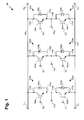
- FIG. 1 shows an exemplary schematic of motor drive inverter 100 (also referred to as a three-phase inverter or a three-phase motor drive inverter) in accordance with an embodiment of the present invention.
- motor drive inverter 100 also referred to as a three-phase inverter or a three-phase motor drive inverter
- FIG. 1 shows an exemplary schematic of motor drive inverter 100 (also referred to as a three-phase inverter or a three-phase motor drive inverter) in accordance with an embodiment of the present invention.
- motor drive inverter 100 also referred to as a three-phase inverter or a three-phase motor drive inverter
- Motor drive inverter 100 may be implemented in a bondwireless power module with a press-fit clamp, although other circuits can be implemented in other embodiments of the present invention.
- Motor drive inverter 100 comprises high side devices 102a, 102b, and 102c and low side devices 102d, 102e, and 102f, which are also referred to herein as devices, such as devices 102a-102f.
- each of devices 102a-102f is a power switch including a freewheeling diode connected in parallel with a corresponding insulated-gated bipolar transistor (IGBT).
- IGBT 104a includes IGBT 104a and diode 106a
- high side device 102b includes IGBT 104b and diode 106b
- high side device 102c includes IGBT 104c and diode 106c
- low side device 102d includes IGBT 104d and diode 106d
- low side device 102e includes IGBT 104e and diode 106e
- low side device 102f includes IGBT 104f and diode 106f.
- devices 102a-102f each include an IGBT as a power switch
- each of devices 102a-102f can include a different device, such as a metal-oxide-semiconductor field-effect transistor (MOSFET).
- MOSFET metal-oxide-semiconductor field-effect transistor
- a MOSFET replaces IGBT 104a and diode 106b can be a body diode of the MOSFET.
- devices 102a-102f may not include diodes 106a-106f or may include electrical components other than diodes 106a-106f
- devices 102a-102f are devices other than power switches.
- Motor drive inverter 100 includes high side power bus 108 and low side power bus 110.
- High side power bus 108 includes high side input power terminals V H1 and V H4 for connecting a high side supply voltage across high side power bus 108 to provide power to motor drive inverter 100.
- Low side power bus 110 includes low side input power terminals V L1 and V L4 for connecting a low side supply voltage across low side power bus 110 to provide power to motor drive inverter 100. Any combination of positive, negative, or ground voltages can be connected to input power terminals V H1 , V H4 , V L1 and V L4 in various embodiments of the present invention.
- motor drive inverter 100 is a three-phase inverter, or more generally a polyphase inverter, which can be used to drive a motor (not shown in Figure 1 ).
- a U phase of motor drive inverter 100 includes devices 102a and 102d connected in a half-bridge between high side power bus 108 and low side power bus 110 with output current terminal U out connected between devices 102a and 102d.
- a V phase of motor drive inverter 100 includes devices 102b and 102e connected in a half-bridge between high side power bus 108 and low side power bus 110 with output current terminal V out connected between devices 102b and 102e.
- a W phase of motor drive inverter 100 includes devices 102c and 102f connected in a half-bridge between high side power bus 108 and low side power bus 110 with output current terminal W out connected between devices 102c and 102f.
- Motor drive inverter 100 also includes high side gate terminals G H1 , G H2 , and G H3 and low side gate terminals G L1 , G L2 , and G L3 (also referred to herein as gate terminals G H1 , G H2 , G H3 , G L1, G L2 , and G L3 ), which are each connected to a corresponding gate of one of IGBTs 104a-104f, as shown in Figure 1 .
- Gate terminals G H1 , G H2 , G H3 , G L1 , G L2 , and G L3 can be used to selectively enable and disable IGBTs 104a-104f, as is known in the art.
- Figure 1 shows collector/cathode nodes 114a, 114b, 114c, 114d, 114e, and 114f and emitter/anode nodes 112a, 112b, 112c, 112d, 112e, and 112f.
- Collector/cathode nodes 114a, 114b, and 114c are each connected to high side power bus 108 and emitter/anode nodes 112d, 112e, and 112f are each connected to low side power bus 110.
- emitter/anode node 112a is connected to collector/cathode node 114d
- emitter/anode node 112b is connected to collector/cathode node 114e
- emitter/anode node 112c is connected to collector/cathode node 114f.
- motor drive inverter 100 has input power terminals V H1 , V H4 , V L1 and V L4 and output current terminals U out , V out , W out , which can support high current and high power.
- Motor drive inverter 100 can be, for example, a motor drive inverter for a motor in a hybrid vehicle.
- the motor drive inverter may generate heat, which can reach input power terminals V H1 , V H4 , V L1 and V L4 and output current terminals U out , V out , W out.
- contacts to input power terminals V H1 , V H4 , V L1 and V L4 and output current terminals U out , V out , W out can reach high temperatures.
- the motor drive inverter will frequently vacillate between periods of use and disuse, thereby exposing the contacts to thermal cycling. Also, body rattle of the hybrid vehicle may cause mechanical stress on the connection of the contacts.
- the contacts may conventionally comprise bond wires or leads that can be affixed respectively to input power terminals V H1 , V H4 , V L1, and V L4 and output current terminals U out , V out , and W out .
- Embodiments of the present invention can provide for press-fit clamps, which can withstand the harsh operating conditions, such as those described above. It will be appreciated that although in the present example the invention is described in relation to a motor drive inverter; in other embodiments, circuits and modules other than a motor drive inverter can benefit from the present invention as disccussed below.
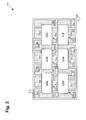
- FIG 2 shows a top view of bondwireless power module 200 (also referred to herein as “three-phase inverter module,” “motor drive inverter module,” and “power module”) residing on substrate 216 prior to connection with at least one press-fit clamp, in accordance with an embodiment of the present invention.
- Bondwireless power module 200 can correspond to motor drive inverter 100 in Figure 1 .
- Figure 2 shows high side conductive clips 218a, 218b, 218c (also referred to herein as “conductive clips 218” and “high side conductive clips 218") and low side conductive clips 218d, 218e, and 218f (also referred to herein as “conductive clips 218” and “low side conductive clips 218"), high side gate pads G H1 , G H2 , G H3 (also referred to herein as “gate pads G” and “high side gate pads G”) and low side gate pads G L1 , G L2 , and G L3 (also referred to herein as “gate pads G” and “low side gate pads G”), high side power pads V H1 , V H2 , V H3 , V H4 (also referred to herein as “power pads V” and “high side power pads V”) and low side power pads V L1 , V L2 , V L3 , and V L4 (also referred to herein as “power pads V” and “low side power pads V”) and
- substrate 216 can comprise for example, insulating material, such as ceramic, epoxy resin, and other substrate materials.
- Gate pads G, power pads V, and output current pads U out , V out , and W out are over substrate 216 and comprise conductive material, such as copper.
- substrate 216 can comprise a direct bonded copper (DBC) substrate.
- DBC direct bonded copper
- substrate 216 can comprise ceramic having copper gate pads G, power pads V, and output current pads U out , V out , and W out bonded to the surface thereof.
- gate pads G, power pads V, and output current pads U out , V out , and W out can comprise conductive traces of substrate 216.
- output current pads U out , V out , and W out are each a single continuous pad in the present embodiment.
- substrate 216 can include a conductive material on bottom surface 226 thereof, which is not shown in Figure 2 .
- the conductive material can be a copper layer bonded to ceramic.
- bottom surface 226 of substrate 216 can comprise dielectric material and in other embodiments bottom surface 226 can comprise conductive material.
- conductive clips 218 comprise conductive material and are over respective gate pads G, power pads V, and output current pads U out , V out , and W out .
- conductive clips 218 can be copper, or other metals or metal alloys.
- Conductive clips 218 include a top surface (shown in Figure 2 ) and opposing legs (not shown in Figure 2 ) connected to the top surface. One of the opposing legs is electrically connecting the top surface to one of power pads V and the other of the opposing legs is electrically connecting the top surface to another of power pads V.
- the opposing legs of conductive clip 218a are respectively electrically connected to high side power pads V H1 and V H2 in regions where conductive clip 218a overlaps power pads V H1 and V H2 in Figure 2 .
- conductive clips 218 are not electrically connected to output current pads U out , V out , and W out and gate pads G. Rather, for example, high side conductive clips 218 and high side power pads V form a current path between high side power pads V H1 and V H4 such that current can traverse through high side conductive clips 218 over output current pads U out , V out , and W out and high side gate pads G.
- high side power pads V H1 and V H4 in Figure 2 can correspond respectively to high side input power terminals V H1 and V H4 in Figure 1 and may be referred to as high side input power pads V H1 and V H4 or simply input power pads V H1 and V H4 .
- a high side power bus corresponding to high side power bus 108 in Figure 1 is formed between input power pads V H1 and V H4 .
- low side conductive clips 218 and low side power pads V form a current path between low side power pads V L1 and V L4 such that current can traverse through low side conductive clips 218 over output current pads U out , V out , and W out and low side gate pads G.
- low side power pads V L1 and V L4 in Figure 2 can correspond respectively to low side input power terminals V L1 and V L4 in Figure 1 and may be referred to as low side input power pads V L1 and V L4 or simply input power pads V L1 and V L4 .
- a low side power bus corresponding to low side power bus 110 in Figure 1 is formed between input power pads V L1 and V L4 .
- high side devices 202a, 202b, and 202c correspond respectively to high side devices 102a, 102b, and 102c in Figure 1 .
- low side devices 202a, 202b, and 202c correspond respectively to low side devices 102d, 102e, and 102f in Figure 1 .
- high side devices 202a, 202b, and 202c and low side devices 202d, 202e, and 202f each comprise a freewheeling diode connected in parallel with a corresponding IGBT.
- the freewheeling diode and the IGBT are not shown in Figure 2 , but can be included under the top surface of a respective conductive clip 218 between the opposing legs discussed above.
- high side conductive clips 218a, 218b, and 218c are electrically connected to respective nodes corresponding respectively to collector/cathode nodes 114a, 114b, and 114c in Figure 1 .
- Low side conductive clips 218d, 218e, and 218f are electrically connected to respective nodes corresponding respectively to emitter/anode nodes 112d, 112e, and 112f in Figure 1 .
- output current pad U out is coupling an emitter/anode node of high side device 202a, corresponding to emitter/anode node 112a in Figure 1 , to a collector/cathode node of low side device 202d, corresponding to collector/cathode node 114d in Figure 1 .
- Output current pad V out is coupling an emitter/anode node of high side device 202b, corresponding to emitter/anode node 112b in Figure 1 , to a collector/cathode node of low side device 202e, corresponding to collector/cathode node 114e in Figure 1 .
- output current pad W out is coupling an emitter/anode node of high side device 202c, corresponding to emitter/anode node 112c in Figure 1 , to a collector/cathode node of low side device 202f, corresponding to collector/cathode node 114f in Figure 1 .
- output current pads U out , V out , and W out in Figure 2 correspond respectively to output current terminals U out , V out , and W out in Figure 1 .
- output current pads U out , V out , and W out are each coupled to a high side device and a low side device where the high and low side devices are connected in a half-bridge, as described above with respect to Figure 1 .
- gate pads G H1 , G H2 , G H3 , G L1 , G L2 , and G L3 correspond respectively to gate terminals G H1 , G H2 , G H3 , G L1 , G L2 , and G L3 in Figure 1 and are each electrically connected to a gate of a corresponding IGBT under a respective conductive clip 218.
- power module 200 comprises a U-phase, a V-phase, and a W-phase of a three-phase inverter.
- Power module 200 comprises input power pads V H1 , V H4 , V L1 , and V L4 and output current pads U out , V out , and W out .
- Power module 200 may also include a respective contact electrically and mechanically connected to each of input power pads V H1 , V H4 , V L1 , and V L4 and output current pads U out , V out , and W out to allow for connection of power module 200 to external circuits (not show in Figure 2 ).
- power module 200 can be a motor drive inverter for a motor in a hybrid vehicle.
- motor drive inverter module 200 will generate heat, which will reach the contacts.
- devices 102 in Figure 1 can generate heat and furthermore, high current will flow through input power pads V H1 , V H4 , V L1 , and V L4 and output current pads U out , V out , and W out and into the contacts resulting in a high temperature in the contacts.
- motor drive inverter module 200 will frequently vacillate between periods of use and disuse, thereby exposing the contacts to thermal cycling. Also, body rattle of the hybrid vehicle may cause mechanical stress on the connection with the contacts.
- power module 200 includes at least one press-fit input power clamp as a contact for at least one of input power pads V H1 , V H4 , V L1 , and V L4 and at least one press-fit output current clamp as a contact for at least one of output current pads U out , V out , and W out , which are capable of withstanding harsh operating conditions, such as those described above, while maintaining electrical and mechanical connection with power module 200.
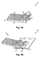
- FIG. 3A illustrates press-fit clamp 340, in accordance with an embodiment of the present invention.
- press-fit clamp 340 is in an disengaged configuration and includes at least one top prong and a least one bottom prong.
- press-fit clamp 340 includes two top prongs and a bottom prong.
- Press-fit clamp 340 includes lead portion 344, top prongs 346a and 346b (also referred to herein as "prongs”), and bottom prong 348 (also referred to herein as "prong").
- lead portion 344 has top surface 350 and adjoining edge 352.
- edge 352 of lead portion 344 is continuous with edge 354 of prong 346b as shown in Figure 3A .
- an edge of prong 346a is continuous with another edge adjoining top surface 350 of lead portion 344 (not shown in Figure 3A ).
- Press-fit clamp 340 comprises conductive material and in the present embodiment is copper. In some embodiments, press-fit clamp 340 can be constructed by lead forming out of a copper block.
- each of prongs 346a, 346b, and 348 include at least one downward bend and at least one upward bend.
- prong 346a has downward bend 356 and upward bend 358.
- Prongs 346a and 346b each have a downward bend opposing an upward bend in prong 348 and an upward bend opposing a downward bend in prong 348, as shown in Figure 3A .
- the upward bends of prongs 346a and 346b e.g. bend 358) are configured to engage a top side of at least one input power pad
- the downward bend of prong 348 is configured to configured to engage a bottom surface of a substrate.
- prongs 346a, 346b, and 348 can have more or less upward or downward bends than shown in Figure 3A , including no upward or downward bends.
- Figure 3B illustrates structure 300 including press-fit clamp 340 engaging contact pad 360 and substrate 316, in accordance with an embodiment of the present invention.
- Substrate 316 corresponds to substrate 216 in Figure 2 and contact pad 360 corresponds to one of gate pads G, power pads V, and output current pads U out , V out , and W out in Figure 2 .
- press-fit clamp 340 is engaging top side 324 of contact pad 360, and engaging bottom surface 326 of substrate 316. More particularly, in the present embodiment, top prongs 346a and 346b are engaging top side 324 of contact pad 360, and bottom prong 348 is engaging bottom surface 326 of substrate 316.
- press-fit clamp 340 is engaged, which can be achieved by receiving substrate 316 and contact pad 360 between top prongs 346a and 346b and bottom prong 348, thereby displacing bottom prong 348 below top prongs 346a and 346b from the disengaged position shown in Figure 3A .
- bottom prong 348 is pressing contact pad 360 into top prongs 346a and 346b to apply a clamping force to contact pad 360 and substrate 316.
- bottom surface 326 of substrate 316 can comprise dielectric material and in other embodiments bottom surface 326 can comprise conductive material.
- bottom surface 326 of substrate 316 comprises dielectric material such that bottom surface 326 is electrically isolated from contact pad 360.
- bottom surface 326 can comprise conductive material and can be electrically connected to contact pad 360.
- substrate 316 can include at least one through via having conductive material electrically connecting contact pad 360 to bottom surface 326 of substrate 316.
- press-fit clamp 340 is a contact affixed to contact pad 360 using a clamping force applied to contact pad 360 and substrate 316.
- Press-fit clamp 340 is configured to maintain good electrical and mechanical contact with contact pad 360 by relying primarily on the clamping force as opposed to solder, conducive adhesive, or other connection means. Although the other connection means may be utilized, they are not required in preferred embodiments of the present invention.
- press-fit clamp 340 can maintain good electrical and mechanical contact with contact pad 360 even when exposed to significant stress.
- press-fit clamp 340 can maintain contact with contact pad 360 when carrying high current and when exposed to high temperatures. Furthermore, good contact can be maintained throughout thermal cycling.
- prongs 346a, 346b, and 348 can adjust to accommodate thermal expansion of substrate 316 and contact pad 360 and can absorb mechanical stress on the connection, for example, due to body rattle in a hybrid vehicle. As such, the connection between press-fit clamp 340 and contact pad 360 is not prone to failing due to bond wire lift off or solder wear out.
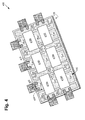
- Figure 4 shows a perspective view illustrating bondwireless power module 400 with press-fit clamps 440a, 440b, 440c, 440d, 440e, 440f, and 440g (also referred to herein as "press-fit clamps 440"), in accordance with an embodiment of the present invention.
- Power module 400 corresponds to power module 200 in Figure 2 .
- conductive clips 418a, 418b, 418c, 418d, 418e, and 418f correspond respectively to conductive clips 218a, 218b, 218c, 218d, 218e, and 218f in Figure 2 .
- gate pads G, power pads V, output current pads U out , V out , and W out and substrate 416 correspond respectively to gate pads G, power pads V, output current pads U out , V out , and W out and substrate 216 in Figure 2 .
- each of press-fit clamps 440 corresponds to a press-fit clamp 340 in Figures 3A and 3B . As shown in Figure 4 , each of press-fit clamps 440 is engaging a top side of a respective contact pad, and engaging a bottom surface of substrate 416, similar to what has been described with respect to press-fit clamp 340, contact pad 360, and substrate 316 in Figure 3B . For example, press-fit clamp 440a is engaging top side 424 of output current pad U out , and engaging bottom surface 426 of substrate 416 (not shown in Figure 4 ).
- press-fit clamps 440 is engaging a top surface of more than one contact pad.
- more than one press-fit clamp is engaging a top surface of the same contact pad.
- power module 400 can include another press-fit clamp engaging top side 424 on opposing side 430 of output current pad U out and power module 400.
- respective press-fit clamps can engage top surfaces of output current pads V out and W out on opposing sides thereof. It is noted that press-fit clamps can engage a top surface of any combination of pads shown in Figure 4 similar to what has been described with respect to Figure 3B and is not limited by the specific embodiment shown in Figure 4 .
- press-fit clamps may engage a top surface of any of gate pads G.
- these press-fit clamps are smaller and have lower current carrying capability than press-fit clamps 440.
- bond wires or other connection means may be used instead of or in addition to press-fit clamps to contact any of the contact pads in Figure 4 , such as gate pads G.
- press-fit clamps 440a, 440b, and 440c are press-fit output current clamps and are respectively engaging a top side of respective output current pads U out , V out , and W out , which can provide output current from power module 400.
- output current pad U out is providing output current 422 from power module 400, which is a high current received by press-fit clamp 440a.
- Press-fit clamps 440a, 440b, and 440c are also providing electrical connection to a first external circuit, which is not shown in Figure 4 .
- the first external circuit can be a motor circuit.
- press-fit clamps 440d, 440e, 440f, and 440g are press-fit input power clamps, and are respectively engaging a top side of respective input power pads V H1 , V H4 , V L1 , and V L4 .
- a high side power bus corresponding to high side power bus 108 in Figure 1 is formed between input power pads V H1 and V H4 .
- the high side power bus is formed between press-fit clamps 440d and 440e.
- a low side power bus corresponding to low side power bus 110 in Figure 1 is formed between input power pads V L1 and V L4 .
- the low side power bus is formed between press-fit clamps 440f and 440g.
- Press-fit clamps 440d, 440e, 440f, and 440g are also providing electrical connection to a second external circuit, which is not shown in Figure 4 .
- the second external circuit can be a control circuit or a regulated power supply for power module 400.
- press-fit clamps 440 are at respective high power and high current input and output terminals in power module 400. As such, contact can be maintained with power module 400 throughout aforementioned harsh operating conditions.
- the present invention can provide for a power module, such as a bondwireless three-phase inverter module with press-fit clamps.
- a power module such as a bondwireless three-phase inverter module with press-fit clamps.
- Various embodiments of the present invention allow for good electrical and mechanical contact between the bondwireless power module and one or more external circuits, which can support high current. The electrical and mechanical contact can be maintained even when exposed to harsh operating conditions. Thus, connection can be made with the bondwireless power module while substantially reducing the risk of contact failure.
Landscapes
- Inverter Devices (AREA)
- Battery Mounting, Suspending (AREA)
Applications Claiming Priority (1)
| Application Number | Priority Date | Filing Date | Title |
|---|---|---|---|
| US13/094,695 US9001518B2 (en) | 2011-04-26 | 2011-04-26 | Power module with press-fit clamps |
Publications (2)
| Publication Number | Publication Date |
|---|---|
| EP2518766A2 true EP2518766A2 (de) | 2012-10-31 |
| EP2518766A3 EP2518766A3 (de) | 2014-03-19 |
Family
ID=45999564
Family Applications (1)
| Application Number | Title | Priority Date | Filing Date |
|---|---|---|---|
| EP20120160152 Ceased EP2518766A3 (de) | 2011-04-26 | 2012-03-19 | Leistungsmodul mit Presspassungsklemmen |
Country Status (2)
| Country | Link |
|---|---|
| US (1) | US9001518B2 (de) |
| EP (1) | EP2518766A3 (de) |
Cited By (4)
| Publication number | Priority date | Publication date | Assignee | Title |
|---|---|---|---|---|
| DE102014203899A1 (de) * | 2014-03-04 | 2015-09-24 | Volkswagen Aktiengesellschaft | Vorrichtung und elektrische Baugruppe zum Wandeln einer Gleichspannung in eine Wechselspannung |
| CN107771416A (zh) * | 2015-06-22 | 2018-03-06 | 瑞典爱立信有限公司 | 用于无埋块的rf功率放大器的滑动和安装制造 |
| US10912185B2 (en) | 2015-06-22 | 2021-02-02 | Telefonaktiebolaget Lm Ericsson (Publ) | Low-cost superior performance coinless RF power amplifier |
| EP3378122B1 (de) * | 2015-11-20 | 2021-10-20 | Shure Acquisition Holdings, Inc. | Wendelantenne für ein drahtloses mikrofon und verfahren dafür |
Families Citing this family (6)
| Publication number | Priority date | Publication date | Assignee | Title |
|---|---|---|---|---|
| US8350376B2 (en) * | 2011-04-18 | 2013-01-08 | International Rectifier Corporation | Bondwireless power module with three-dimensional current routing |
| CN103066042B (zh) * | 2012-12-31 | 2015-07-15 | 江苏宏微科技股份有限公司 | 功率模块电极端子的连接结构 |
| US10566713B2 (en) | 2018-01-09 | 2020-02-18 | Semiconductor Components Industries, Llc | Press-fit power module and related methods |
| US10925166B1 (en) * | 2019-08-07 | 2021-02-16 | Quanta Computer Inc. | Protection fixture |
| KR102802515B1 (ko) * | 2019-12-10 | 2025-05-02 | 엘지디스플레이 주식회사 | 인쇄회로기판 및 이를 포함하는 표시장치 |
| TWD206651S (zh) | 2020-04-24 | 2020-08-21 | 財團法人工業技術研究院 | 功率模組 |
Citations (3)
| Publication number | Priority date | Publication date | Assignee | Title |
|---|---|---|---|---|
| US20050189566A1 (en) * | 2002-12-27 | 2005-09-01 | Murata Manufacturing Co., Ltd. | Switching power-supply module |
| US20060071238A1 (en) * | 2004-09-23 | 2006-04-06 | Alberto Guerra | Power module |
| US20070246812A1 (en) * | 2006-04-25 | 2007-10-25 | International Rectifier Corporation | High reliability power module |
Family Cites Families (13)
| Publication number | Priority date | Publication date | Assignee | Title |
|---|---|---|---|---|
| GB1369995A (en) | 1972-08-25 | 1974-10-09 | Int Computers Ltd | Electrical connecting devices |
| US4579406A (en) * | 1985-01-11 | 1986-04-01 | D.A.V.I.D. Systems, Inc. | Printed circuit board connector system |
| JPH0828557B2 (ja) * | 1987-10-29 | 1996-03-21 | 株式会社日立製作所 | 基板の電源配線構造 |
| FR2625040B1 (fr) | 1987-12-22 | 1991-01-04 | Cit Alcatel | Plot de report de connexion pour la fixation d'une broche a griffes sur la tranche d'un substrat de circuit hybride |
| US6586684B2 (en) * | 2001-06-29 | 2003-07-01 | Intel Corporation | Circuit housing clamp and method of manufacture therefor |
| DE102004036982B4 (de) | 2004-07-30 | 2010-07-29 | Infineon Technologies Ag | Leistungshalbleitermodulsystem mit einem in einen Baugruppenträger einsteckbaren und mit einem Gehäuse des Baugruppenträgers verrastbaren Leistungshalbleitermodul |
| US8018056B2 (en) | 2005-12-21 | 2011-09-13 | International Rectifier Corporation | Package for high power density devices |
| US7554188B2 (en) | 2006-04-13 | 2009-06-30 | International Rectifier Corporation | Low inductance bond-wireless co-package for high power density devices, especially for IGBTs and diodes |
| US7619302B2 (en) | 2006-05-23 | 2009-11-17 | International Rectifier Corporation | Highly efficient both-side-cooled discrete power package, especially basic element for innovative power modules |
| US8680666B2 (en) | 2006-05-24 | 2014-03-25 | International Rectifier Corporation | Bond wireless power module with double-sided single device cooling and immersion bath cooling |
| US8059404B2 (en) * | 2008-10-09 | 2011-11-15 | GM Global Technology Operations LLC | Power inverters |
| JP5550927B2 (ja) * | 2010-01-29 | 2014-07-16 | 本田技研工業株式会社 | 電力変換装置 |
| DE102010013138A1 (de) * | 2010-03-27 | 2011-09-29 | Semikron Elektronik Gmbh & Co. Kg | Schaltungsanordnung und Verfahren zur Erzeugung einer Wechselspannung aus einer Mehrzahl von Spannungsquellen mit zeitlich variabler Ausgangsgleichspannung |
-
2011
- 2011-04-26 US US13/094,695 patent/US9001518B2/en active Active
-
2012
- 2012-03-19 EP EP20120160152 patent/EP2518766A3/de not_active Ceased
Patent Citations (3)
| Publication number | Priority date | Publication date | Assignee | Title |
|---|---|---|---|---|
| US20050189566A1 (en) * | 2002-12-27 | 2005-09-01 | Murata Manufacturing Co., Ltd. | Switching power-supply module |
| US20060071238A1 (en) * | 2004-09-23 | 2006-04-06 | Alberto Guerra | Power module |
| US20070246812A1 (en) * | 2006-04-25 | 2007-10-25 | International Rectifier Corporation | High reliability power module |
Cited By (7)
| Publication number | Priority date | Publication date | Assignee | Title |
|---|---|---|---|---|
| DE102014203899A1 (de) * | 2014-03-04 | 2015-09-24 | Volkswagen Aktiengesellschaft | Vorrichtung und elektrische Baugruppe zum Wandeln einer Gleichspannung in eine Wechselspannung |
| DE102014203899B4 (de) * | 2014-03-04 | 2024-03-14 | Volkswagen Aktiengesellschaft | Vorrichtung und elektrische Baugruppe zum Wandeln einer Gleichspannung in eine Wechselspannung |
| CN107771416A (zh) * | 2015-06-22 | 2018-03-06 | 瑞典爱立信有限公司 | 用于无埋块的rf功率放大器的滑动和安装制造 |
| US10842028B2 (en) | 2015-06-22 | 2020-11-17 | Telefonaktiebolaget Lm Ericsson (Publ) | Method for mounting a power amplifier (AP) assembly |
| US10912185B2 (en) | 2015-06-22 | 2021-02-02 | Telefonaktiebolaget Lm Ericsson (Publ) | Low-cost superior performance coinless RF power amplifier |
| EP3378122B1 (de) * | 2015-11-20 | 2021-10-20 | Shure Acquisition Holdings, Inc. | Wendelantenne für ein drahtloses mikrofon und verfahren dafür |
| US11251519B2 (en) | 2015-11-20 | 2022-02-15 | Shure Acquisition Holdings, Inc. | Helical antenna for wireless microphone and method for the same |
Also Published As
| Publication number | Publication date |
|---|---|
| US9001518B2 (en) | 2015-04-07 |
| US20120275121A1 (en) | 2012-11-01 |
| EP2518766A3 (de) | 2014-03-19 |
Similar Documents
| Publication | Publication Date | Title |
|---|---|---|
| US9001518B2 (en) | Power module with press-fit clamps | |
| US9490200B2 (en) | Semiconductor device | |
| US9129932B2 (en) | Semiconductor module | |
| US8987777B2 (en) | Stacked half-bridge power module | |
| KR101755769B1 (ko) | 양면 냉각 파워 모듈 및 이의 제조 방법 | |
| CN110235244B (zh) | 功率半导体模块以及电力转换装置 | |
| US8804340B2 (en) | Power semiconductor package with double-sided cooling | |
| US8237260B2 (en) | Power semiconductor module with segmented base plate | |
| US10002837B2 (en) | Semiconductor device | |
| US9653386B2 (en) | Compact multi-die power semiconductor package | |
| US11244836B2 (en) | Semiconductor apparatus, power conversion device, and method for manufacturing semiconductor apparatus | |
| CN109417066B (zh) | 半导体装置 | |
| CN102254895B (zh) | 半导体装置,半导体单元和电力用半导体装置 | |
| CN109727960A (zh) | 半导体模块、其制造方法以及电力变换装置 | |
| JP4164409B2 (ja) | 半導体パワーモジュール | |
| US20120262100A1 (en) | Bondwireless Power Module with Three-Dimensional Current Routing | |
| US20160105004A1 (en) | Power Module, Power Converter and Drive Arrangement With A Power Module | |
| CN110178304A (zh) | 半导体装置 | |
| JP2018073923A (ja) | 電力用半導体装置、電力用半導体装置の製造方法および電力変換装置 | |
| KR101734712B1 (ko) | 파워모듈 | |
| JP2015186438A (ja) | 半導体装置 | |
| JP2013045847A (ja) | 半導体モジュール | |
| JP2013098343A (ja) | 半導体装置とその製造方法 | |
| US20250014972A1 (en) | Package with clip directly connected to oblong electric connection element extending along mounting base | |
| KR102940062B1 (ko) | 전력반도체 모듈 |
Legal Events
| Date | Code | Title | Description |
|---|---|---|---|
| PUAI | Public reference made under article 153(3) epc to a published international application that has entered the european phase |
Free format text: ORIGINAL CODE: 0009012 |
|
| AK | Designated contracting states |
Kind code of ref document: A2 Designated state(s): AL AT BE BG CH CY CZ DE DK EE ES FI FR GB GR HR HU IE IS IT LI LT LU LV MC MK MT NL NO PL PT RO RS SE SI SK SM TR |
|
| AX | Request for extension of the european patent |
Extension state: BA ME |
|
| PUAL | Search report despatched |
Free format text: ORIGINAL CODE: 0009013 |
|
| AK | Designated contracting states |
Kind code of ref document: A3 Designated state(s): AL AT BE BG CH CY CZ DE DK EE ES FI FR GB GR HR HU IE IS IT LI LT LU LV MC MK MT NL NO PL PT RO RS SE SI SK SM TR |
|
| AX | Request for extension of the european patent |
Extension state: BA ME |
|
| RIC1 | Information provided on ipc code assigned before grant |
Ipc: H01L 23/48 20060101ALI20140212BHEP Ipc: H01L 25/07 20060101AFI20140212BHEP Ipc: H01L 25/18 20060101ALI20140212BHEP |
|
| 17P | Request for examination filed |
Effective date: 20140919 |
|
| RBV | Designated contracting states (corrected) |
Designated state(s): AL AT BE BG CH CY CZ DE DK EE ES FI FR GB GR HR HU IE IS IT LI LT LU LV MC MK MT NL NO PL PT RO RS SE SI SK SM TR |
|
| 17Q | First examination report despatched |
Effective date: 20170119 |
|
| RAP1 | Party data changed (applicant data changed or rights of an application transferred) |
Owner name: INFINEON TECHNOLOGIES AMERICAS CORP. |
|
| STAA | Information on the status of an ep patent application or granted ep patent |
Free format text: STATUS: THE APPLICATION HAS BEEN REFUSED |
|
| 18R | Application refused |
Effective date: 20190321 |