EP2520944A2 - Batteriezellenimpedanzmessverfahren und Vorrichtung - Google Patents
Batteriezellenimpedanzmessverfahren und Vorrichtung Download PDFInfo
- Publication number
- EP2520944A2 EP2520944A2 EP20120166398 EP12166398A EP2520944A2 EP 2520944 A2 EP2520944 A2 EP 2520944A2 EP 20120166398 EP20120166398 EP 20120166398 EP 12166398 A EP12166398 A EP 12166398A EP 2520944 A2 EP2520944 A2 EP 2520944A2
- Authority
- EP
- European Patent Office
- Prior art keywords
- circuit
- waveform
- cell
- cosine
- real
- Prior art date
- Legal status (The legal status is an assumption and is not a legal conclusion. Google has not performed a legal analysis and makes no representation as to the accuracy of the status listed.)
- Granted
Links
Images


Classifications
-
- G—PHYSICS
- G01—MEASURING; TESTING
- G01R—MEASURING ELECTRIC VARIABLES; MEASURING MAGNETIC VARIABLES
- G01R31/00—Arrangements for testing electric properties; Arrangements for locating electric faults; Arrangements for electrical testing characterised by what is being tested not provided for elsewhere
- G01R31/36—Arrangements for testing, measuring or monitoring the electrical condition of accumulators or electric batteries, e.g. capacity or state of charge [SoC]
- G01R31/389—Measuring internal impedance, internal conductance or related variables
-
- H—ELECTRICITY
- H01—ELECTRIC ELEMENTS
- H01M—PROCESSES OR MEANS, e.g. BATTERIES, FOR THE DIRECT CONVERSION OF CHEMICAL ENERGY INTO ELECTRICAL ENERGY
- H01M10/00—Secondary cells; Manufacture thereof
- H01M10/42—Methods or arrangements for servicing or maintenance of secondary cells or secondary half-cells
- H01M10/44—Methods for charging or discharging
-
- H—ELECTRICITY
- H01—ELECTRIC ELEMENTS
- H01M—PROCESSES OR MEANS, e.g. BATTERIES, FOR THE DIRECT CONVERSION OF CHEMICAL ENERGY INTO ELECTRICAL ENERGY
- H01M10/00—Secondary cells; Manufacture thereof
- H01M10/42—Methods or arrangements for servicing or maintenance of secondary cells or secondary half-cells
- H01M10/48—Accumulators combined with arrangements for measuring, testing or indicating the condition of cells, e.g. the level or density of the electrolyte
- H01M10/482—Accumulators combined with arrangements for measuring, testing or indicating the condition of cells, e.g. the level or density of the electrolyte for several batteries or cells simultaneously or sequentially
-
- H—ELECTRICITY
- H02—GENERATION; CONVERSION OR DISTRIBUTION OF ELECTRIC POWER
- H02J—ELECTRIC POWER NETWORKS; CIRCUIT ARRANGEMENTS OR SYSTEMS FOR SUPPLYING OR DISTRIBUTING ELECTRIC POWER; SYSTEMS FOR STORING ELECTRIC ENERGY
- H02J7/00—Circuit arrangements for charging or discharging batteries or for supplying loads from batteries
- H02J7/50—Circuit arrangements for charging or discharging batteries or for supplying loads from batteries acting upon multiple batteries simultaneously or sequentially
- H02J7/52—Circuit arrangements for charging or discharging batteries or for supplying loads from batteries acting upon multiple batteries simultaneously or sequentially for charge balancing, e.g. equalisation of charge between batteries
- H02J7/56—Active balancing, e.g. using capacitor-based, inductor-based or DC-DC converters
-
- H—ELECTRICITY
- H01—ELECTRIC ELEMENTS
- H01M—PROCESSES OR MEANS, e.g. BATTERIES, FOR THE DIRECT CONVERSION OF CHEMICAL ENERGY INTO ELECTRICAL ENERGY
- H01M10/00—Secondary cells; Manufacture thereof
- H01M10/42—Methods or arrangements for servicing or maintenance of secondary cells or secondary half-cells
- H01M10/425—Structural combination with electronic components, e.g. electronic circuits integrated to the outside of the casing
- H01M2010/4271—Battery management systems including electronic circuits, e.g. control of current or voltage to keep battery in healthy state, cell balancing
-
- Y—GENERAL TAGGING OF NEW TECHNOLOGICAL DEVELOPMENTS; GENERAL TAGGING OF CROSS-SECTIONAL TECHNOLOGIES SPANNING OVER SEVERAL SECTIONS OF THE IPC; TECHNICAL SUBJECTS COVERED BY FORMER USPC CROSS-REFERENCE ART COLLECTIONS [XRACs] AND DIGESTS
- Y02—TECHNOLOGIES OR APPLICATIONS FOR MITIGATION OR ADAPTATION AGAINST CLIMATE CHANGE
- Y02E—REDUCTION OF GREENHOUSE GAS [GHG] EMISSIONS, RELATED TO ENERGY GENERATION, TRANSMISSION OR DISTRIBUTION
- Y02E60/00—Enabling technologies; Technologies with a potential or indirect contribution to GHG emissions mitigation
- Y02E60/10—Energy storage using batteries
-
- Y—GENERAL TAGGING OF NEW TECHNOLOGICAL DEVELOPMENTS; GENERAL TAGGING OF CROSS-SECTIONAL TECHNOLOGIES SPANNING OVER SEVERAL SECTIONS OF THE IPC; TECHNICAL SUBJECTS COVERED BY FORMER USPC CROSS-REFERENCE ART COLLECTIONS [XRACs] AND DIGESTS
- Y02—TECHNOLOGIES OR APPLICATIONS FOR MITIGATION OR ADAPTATION AGAINST CLIMATE CHANGE
- Y02T—CLIMATE CHANGE MITIGATION TECHNOLOGIES RELATED TO TRANSPORTATION
- Y02T10/00—Road transport of goods or passengers
- Y02T10/60—Other road transportation technologies with climate change mitigation effect
- Y02T10/70—Energy storage systems for electromobility, e.g. batteries
Definitions
- SoC State of Charge
- the SoCs of the battery cells will not be the same and drift apart over time, after charging and discharging. If no action is taken, the differences will grow with each charge/discharge cycle, leading to a reduction of the useable battery capacity and life time.
- SoCs can cause a battery cell to be over-discharged during use or over-charged in the charging process.
- over-charging or over-discharging may damage the battery cell.
- a fully charged lithium ion cell often has a voltage that is close to the electrolyte breakdown threshold voltage at which damage to the cell may occur. If a cell is over-charged to the point where the voltage exceeds the electrolyte breakdown threshold voltage, the cell may be damaged.
- battery packs of series-coupled cells often include cell-balancing circuits that equalize the SoCs between the series-coupled cells. By balancing the SoCs of the cells at rest, during charge or discharge, cells may be prevented from becoming over-charged or over-discharged.
- Impedance of the cell(s) helps to accurately estimate the SoC, state of function (SoF) and the state of health (SoH) of the battery pack. Impedance may also be used to implement optimal charge and discharge strategies to maximize battery life, cycle life, and utilize the available energy storage capacity of the battery pack.
- Electroscopy is a technique that determines the impedance of the battery at different frequencies.
- a source drives a current through the battery pack.
- the source may be either a voltage source or a current source.
- the voltage and/or current driven through a battery cell typically has a low amplitude, such that the battery can be regarded as a linear system at the measurement point.
- the current is converted into a voltage by a resistor connected in series with the battery.
- Band-pass filters eliminate unwanted signals (e.g. noise and distortion) before they can reach the amplitude and phase meters.
- the voltages across the battery and conversion resistor are measured with identical amplitude and phase meters. All meters and band-pass filters are identical to ensure equal gain and delay time in these circuits.
- One or more embodiments may address one or more of the above issues.
- a circuit arrangement for determining impedance of a battery cell is provided.
- a first circuit is configured to generate sample values representative of a sine waveform and a cosine waveform. N sample values are used to represent each period of the respective sine and cosine waveforms.
- a second circuit is coupled to an output of the first circuit and is configured to input a current into the battery cell in response to the sample values of the cosine waveform. The current has an amplitude proportional to the sample values of the cosine waveform.
- a third circuit is coupled to the cell and configured to sample voltage levels across the cell resulting from the current being input into the cell.
- a fourth circuit is coupled to an output of the third circuit and is configured to separate each voltage level sampled by the third circuit into real and imaginary components.
- a method for determining impedance of a battery cell Sine and cosine waveforms having N sample points per period are generated. For each sample point of the cosine waveform, a current having an amplitude corresponding to a value of the sample point is injected into a battery cell. A voltage level across the cell is measured and converted from an analog to a digital value. The digital value of the voltage is separated into real and imaginary components. The real component ofN digital values are summed to determine a real component of the impedance of the battery cell. The imaginary component of the N digital values are summed to determine an imaginary component of the impedance of the battery cell.
- an energy storage cell arrangement in yet another embodiment, includes a plurality of battery cells coupled in series and an impedance detection circuit coupled to one of the plurality of battery cells.
- the impedance detection circuit includes a first circuit configured to generate sample values representative of a sine waveform and a cosine waveform. N sample values represent each period of the sine and cosine waveforms.
- a second circuit is coupled to an output of the first circuit and is configured to input a current into the one of the plurality of battery cells in response to the sample values of the cosine waveform. The current injected into the cell has an amplitude proportional to the sample values of the cosine waveform.
- a third circuit is coupled to the one of the plurality of battery cells and is configured to sample voltage levels across the one battery cell resulting from the current being input into the one battery cell.
- a fourth circuit is coupled to an output of the third circuit and is configured to multiply each voltage level sampled by the third circuit with a sine waveform to generate the imaginary component and multiply each voltage level sampled by the third circuit with a cosine waveform to generate the real component.
- the real component of N of the voltage levels sampled by the third circuit are summed to determine a real component of the impedance of the one battery cell.
- the imaginary component ofN of the voltage levels sampled are summed to determine an imaginary component of the impedance of the one battery cell.
- the cell impedance is determined by modulating current through a cell according to known frequency spectrum. Resulting voltages exhibited across the cell are digitized and processed to derive the cell impedances.
- FIG. 1 shows a flowchart of a method for determining impedance of a battery cell(s).
- Corresponding sine and cosine waveforms are generated at block 102.
- Each of the waveforms include N sample points per period.
- a current pulse having an amplitude corresponding to the sample point is injected into a battery cell under test at block 104.
- a voltage exhibited across the cell as a result of the injection of the current is measured and digitized at block 106.
- Each digitized voltage is separated into real and imaginary components at block 110.
- the digitized voltage is separated into respective real and imaginary components by multiplying the digitized voltage by the sample point of the waveforms used to generate the injected current.
- Multiplication of the digitized voltage with the corresponding sample point of the cosine waveform produces the real component of the digitized voltage.
- Multiplication of the digitized voltage with the corresponding sample point of the sine waveform produces the imaginary component of the digitized voltage.
- Real and imaginary components are respectively accumulated for one or more periods of the cosine waveform at block 112 to produce the final real and imaginary parts of the cell impedance.
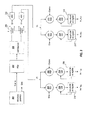
- FIG. 2 shows a circuit that calculates the cell impedance using the process of FIG. 1 .
- a battery pack having a number of cells 208 is implemented with a cell balancing circuit 206.
- a current injected into the cell by the cell-balancer is controlled according to a known waveform.
- a voltage resulting from the injected current can be compared with the known waveform to determine impedance.
- the circuit includes a waveform generator 202 that is configured to generate respective sine and cosine waveforms at a target frequency and sample rate. In some alternative embodiments, samples of the waveforms may be retrieved from a lookup table (LUT).
- LUT lookup table
- pulse density modulator (PDM) circuit 204 For each sample of a cosine waveform produced by waveform generator 202, pulse density modulator (PDM) circuit 204 causes cell balancer circuit 206 to inject a current pulse having a density proportional to the amplitude of the cosine waveform sample. A voltage is produced across the cell 208 as a result of the current pulse, and the voltage is measured and digitized by analog-to-digital converter (ADC) circuit 210. Each digitized voltage produced by the ADC 210 is separated into real and imaginary components using multiplication circuits 212 to multiply the digitized voltage by a corresponding sample of the respective sine and cosine waveforms.
- ADC analog-to-digital converter
- the real component is isolated by multiplying 212 the digitized voltage with a scaled sample of the particular sample point of the cosine waveform generated by the waveform generator 202 and used to create the current pulse in cell 208 that resulted in the particular measured voltage.
- the imaginary component is isolated by multiplying the digitized voltage with the corresponding sample of the sine waveform produced by the waveform generator 202 that is scaled by a calibration scalar. Scaling of the waveforms with a calibration scalar (not shown) is described in detail below.
- the real and imaginary components are respectively accumulated for one or more periods of the cosine waveform by respective accumulators implemented with addition circuit 214 and accumulation register 216. As a result of the accumulation, real and imaginary portions of impedance of the cell are produced.
- one or more alternative embodiments may modulate a current drawn from the cell by a load with the known waveform.
- one or more alternative embodiments may use the generated sine waveform to control current pulses.
- a real component of the digitized voltage is isolated by multiplication of the digitized voltage with the scaled sine waveform.
- an imaginary component of the digitized voltage is isolated by the multiplication of the digitized voltage with the scaled cosine waveform.
- the coefficients of matrix A correspond to the DC voltage offset ( C ) and the amplitude of the generated sine and cosine waveforms.
- Matrix A is constructed from the samples of generated sine and cosine waveforms over one period.
- Matrix A includes a row corresponding to each phase ⁇ of the period.
- the first column includes DC voltage offsets corresponding to each phase ⁇ .
- the DC voltage offsets can be assumed to be one.
- the second column corresponds to the amplitudes of the samples of the generated cosine waveform
- the third column corresponds to the amplitudes of the samples of the generated sine waveform.
- the matrix M may be calculated from the original sampling matrix A. It is recognized that the rows of matrix M have interesting properties. For example, the values of the first row are constant, all the same and equal to one over the number of samples in the data set (i.e., 1/N). The second row is a scaled version of the cosine and the third row is a scaled version of the sine.
- the summation process must include exactly one or more complete cycles of the sine waveform. The result is proportional to the real and imaginary parts of the cell impedance at the measured frequency.
- a calibration scalar is required to find the absolute values of Re(Z) and Im(Z).
- the values C1..Cn and S1..Sn which are the same values used in matrix A, are scaled by 2/N to find the absolute values of Re(Z) and Im(Z).
- the sampled voltage from the ADC 210 is multiplied with scaled samples of the sine and cosine waveforms produced by the waveform generator 202. All sample points in a period of the waveforms are represented by respective second and third rows of matrix A T , with each column corresponding to a phase of the period. Scaling of all of the sample points corresponds to the multiplication of matrix A T by ( A T A ) -1 shown in the above equations.
- the accumulation of the real components performed by the circuit is equivalent to the multiplication of the second row of matrix M with vector b.
- the accumulation of the imaginary components is equivalent to the multiplication of the third row of matrix M with vector 6.
- ADC 210 a column of matrix M is multiplied with the vector b by multiplication circuits 212.
- the resulting products are added to the previously stored values in the real and imaginary accumulator registers 216. For example, when the first sample y 0 of vector b arrives, it is multiplied by the first column of the matrix M and stored in the vector x.
- the first row of the matrix M is constant and equal to (1/N).
- the accumulated DC value of the cell voltage in one period is equal to one.
- the DC value is discarded for spectroscopy, and therefore, the DC accumulator is not required to be implemented in hardware.
- FIG. 3 shows an efficient example implementation of a waveform generator that may be used to generate desired sine and cosine waveforms.
- the circuit generates sine and cosine waveforms using six polynomial coefficients (C0 ... C5).
- the coefficients may be fixed and can be hardwired inside the IC. Alternately, the coefficients may be adjustable to set the generated waveforms to a frequency of interest.
- Each accumulation register 304 is coupled to an adder 306, and together the accumulation register and adder form an accumulator.
- Each subsequent sample is generated by propagating accumulated values between neighboring accumulators. For example, all accumulators will receive a new value that is equal to the sum of their current value and the value of the accumulation register corresponding to the next higher order polynomial coefficient.
- the vectors y n and y n +1 describe the values stored in the accumulators before and after one accumulation step.
- the matrix represents the addition operation.
- the values of the accumulators can also be calculated after (n) steps starting from the initial values given by vector y o (determined by the coefficients co ... c 5 ).
- the output of the first accumulator 310 which corresponds to the first polynomial coefficient, produces the generated sine waveform.
- the output of the second accumulator 312, which corresponds to the first polynomial coefficient, is approximately equal to the first derivative of the output of the first accumulator 310, and may be used to produce the cosine waveform.
- the second accumulator 312 provides a good approximation for the first derivative. Because samples are accumulated over an entire period, any error induced in the approximation of the derivative will statistically be averaged out. Therefore, the circuit shown in FIG. 3 provides a hardware-efficient implementation of the waveform generator.
Landscapes
- Engineering & Computer Science (AREA)
- Manufacturing & Machinery (AREA)
- Chemical & Material Sciences (AREA)
- Chemical Kinetics & Catalysis (AREA)
- Electrochemistry (AREA)
- General Chemical & Material Sciences (AREA)
- Power Engineering (AREA)
- Physics & Mathematics (AREA)
- General Physics & Mathematics (AREA)
- Measurement Of Resistance Or Impedance (AREA)
- Secondary Cells (AREA)
Applications Claiming Priority (1)
| Application Number | Priority Date | Filing Date | Title |
|---|---|---|---|
| US13/100,652 US9128165B2 (en) | 2011-05-04 | 2011-05-04 | Battery cell impedance measurement method and apparatus |
Publications (3)
| Publication Number | Publication Date |
|---|---|
| EP2520944A2 true EP2520944A2 (de) | 2012-11-07 |
| EP2520944A3 EP2520944A3 (de) | 2017-05-03 |
| EP2520944B1 EP2520944B1 (de) | 2023-06-28 |
Family
ID=46001032
Family Applications (1)
| Application Number | Title | Priority Date | Filing Date |
|---|---|---|---|
| EP12166398.3A Active EP2520944B1 (de) | 2011-05-04 | 2012-05-02 | Batteriezellenimpedanzmessverfahren und Vorrichtung |
Country Status (4)
| Country | Link |
|---|---|
| US (1) | US9128165B2 (de) |
| EP (1) | EP2520944B1 (de) |
| CN (1) | CN102768305A (de) |
| ES (1) | ES2957172T3 (de) |
Cited By (2)
| Publication number | Priority date | Publication date | Assignee | Title |
|---|---|---|---|---|
| WO2015014764A3 (de) * | 2013-07-30 | 2015-04-02 | Robert Bosch Gmbh | Elektrochemisches speichermodul und verfahren zur untersuchung einer elektrochemischen speicherzelle in einem modul |
| FR3016701A1 (fr) * | 2014-01-22 | 2015-07-24 | Commissariat Energie Atomique | Procede et dispositif de determination de l'impedance d'un element de stockage d'energie d'une batterie |
Families Citing this family (10)
| Publication number | Priority date | Publication date | Assignee | Title |
|---|---|---|---|---|
| CA2939987C (en) * | 2014-02-19 | 2017-11-21 | Nissan Motor Co., Ltd. | Impedance measuring device and control method for impedance measuring device |
| CN105992956B (zh) * | 2014-02-19 | 2018-11-06 | 日产自动车株式会社 | 阻抗测定装置和阻抗测定装置的控制方法 |
| US9718455B2 (en) * | 2014-02-20 | 2017-08-01 | Ford Global Technologies, Llc | Active battery parameter identification using conditional extended kalman filter |
| US9673657B2 (en) | 2014-04-03 | 2017-06-06 | Nxp B.V. | Battery charging apparatus and approach |
| DE102015218797A1 (de) * | 2015-09-29 | 2017-03-30 | Continental Automotive Gmbh | Verfahren zum Bestimmen eines Realteils eines komplexen Innenwiderstands einer Batterie |
| US10481214B2 (en) * | 2017-01-30 | 2019-11-19 | Infineon Technologies Ag | Battery temperature detection |
| JP7172838B2 (ja) * | 2019-04-26 | 2022-11-16 | 株式会社デンソー | 電池監視装置 |
| EP3812780B1 (de) * | 2019-10-23 | 2022-09-28 | Novum engineerING GmbH | Schätzung eines batteriezustands aus gradienten elektrischer impedanzmessungen |
| CN113030738B (zh) * | 2020-02-18 | 2022-09-16 | 深圳大学 | 一种电池故障检测方法、电池故障检测系统及终端 |
| US12135358B2 (en) * | 2022-12-15 | 2024-11-05 | Nxp B.V. | Non steady state energy cell impedance measurement |
Family Cites Families (27)
| Publication number | Priority date | Publication date | Assignee | Title |
|---|---|---|---|---|
| US3967100A (en) | 1973-11-12 | 1976-06-29 | Naonobu Shimomura | Digital function generator utilizing cascade accumulation |
| JPS5177047A (de) | 1974-12-27 | 1976-07-03 | Naonobu Shimomura | |
| US4510437A (en) * | 1980-10-06 | 1985-04-09 | University Of Utah | Apparatus and method for measuring the permittivity of a substance |
| JP2554511B2 (ja) * | 1987-11-30 | 1996-11-13 | 日本ヒューレット・パッカード株式会社 | ベクトル電流計 |
| JP3608952B2 (ja) * | 1998-07-30 | 2005-01-12 | Necエレクトロニクス株式会社 | インピーダンス測定装置およびインピーダンス測定方法 |
| US6037777A (en) * | 1998-09-11 | 2000-03-14 | Champlin; Keith S. | Method and apparatus for determining battery properties from complex impedance/admittance |
| US6002238A (en) * | 1998-09-11 | 1999-12-14 | Champlin; Keith S. | Method and apparatus for measuring complex impedance of cells and batteries |
| US6262563B1 (en) * | 1998-09-11 | 2001-07-17 | Keith S. Champlin | Method and apparatus for measuring complex admittance of cells and batteries |
| CN1184484C (zh) | 1999-12-20 | 2005-01-12 | 恩益禧电子股份有限公司 | 用来精确测量阻抗的装置及方法 |
| EP1118865A1 (de) * | 2000-01-20 | 2001-07-25 | STMicroelectronics S.r.l. | Schaltung und Verfahren zur Detektierung einer Lastimpedanz |
| TW546480B (en) * | 2000-03-07 | 2003-08-11 | Sumitomo Metal Ind | Circuit, apparatus and method for inspecting impedance |
| DE60007528T2 (de) * | 2000-10-17 | 2004-12-23 | Telefonaktiebolaget L M Ericsson (Publ) | Batteriebetriebenes Gerät mit Ladezustandsanzeige |
| US6778913B2 (en) | 2002-04-29 | 2004-08-17 | Cadex Electronics Inc. | Multiple model systems and methods for testing electrochemical systems |
| FR2842305B1 (fr) * | 2002-07-15 | 2004-10-01 | Inst Nat Polytech Grenoble | Procede de determination de l'independance d'un systeme electrochimique |
| US7619390B2 (en) * | 2003-12-04 | 2009-11-17 | Powertron Eng'g Co., Ltd. | Battery cell voltage and impedance measuring circuit |
| TW200525869A (en) * | 2004-01-28 | 2005-08-01 | Renesas Tech Corp | Switching power supply and semiconductor IC |
| US7019542B2 (en) | 2004-04-06 | 2006-03-28 | Cadex Electronics Inc. | Method and apparatus for battery testing |
| JP5092218B2 (ja) | 2005-09-06 | 2012-12-05 | 富士通株式会社 | 電池パックの異常検出方法、電池パック及び電子機器 |
| KR100812760B1 (ko) * | 2005-12-08 | 2008-03-12 | 김득수 | 축전지 내부 임피던스 유효성분 측정연산 장치 및 그 방법 |
| WO2007143786A1 (en) * | 2006-06-16 | 2007-12-21 | Inphaze Pty Ltd | A system for complex impedance measurement |
| US7965061B2 (en) * | 2008-02-01 | 2011-06-21 | O2Micro, Inc. | Conversion systems with balanced cell currents |
| DE102009002465A1 (de) * | 2009-04-17 | 2010-10-21 | Robert Bosch Gmbh | Ermittlung des Innenwiderstands einer Batteriezelle einer Traktionsbatterie bei Einsatz von resistivem Zellbalancing |
| DE102009051233B4 (de) * | 2009-10-29 | 2017-11-16 | Texas Instruments Deutschland Gmbh | Elektronische Vorrichtung und Verfahren zur Impedanzmessung |
| FR2956743B1 (fr) * | 2010-02-25 | 2012-10-05 | Inst Francais Du Petrole | Procede non intrusif de determination de l'impedance electrique d'une batterie |
| EP2363935B1 (de) | 2010-03-04 | 2013-05-15 | Nxp B.V. | Ausgleichsschaltung für Ladungsspeicherelemente |
| EP2400622A3 (de) | 2010-06-28 | 2012-03-14 | Nxp B.V. | Induktiver Zellenausgleich |
| EP2447728B1 (de) | 2010-10-28 | 2013-06-19 | Nxp B.V. | Messanordnung für Impedanzspektroskopie in Batteriezellen |
-
2011
- 2011-05-04 US US13/100,652 patent/US9128165B2/en active Active
-
2012
- 2012-04-28 CN CN2012101351364A patent/CN102768305A/zh active Pending
- 2012-05-02 ES ES12166398T patent/ES2957172T3/es active Active
- 2012-05-02 EP EP12166398.3A patent/EP2520944B1/de active Active
Non-Patent Citations (1)
| Title |
|---|
| None |
Cited By (3)
| Publication number | Priority date | Publication date | Assignee | Title |
|---|---|---|---|---|
| WO2015014764A3 (de) * | 2013-07-30 | 2015-04-02 | Robert Bosch Gmbh | Elektrochemisches speichermodul und verfahren zur untersuchung einer elektrochemischen speicherzelle in einem modul |
| FR3016701A1 (fr) * | 2014-01-22 | 2015-07-24 | Commissariat Energie Atomique | Procede et dispositif de determination de l'impedance d'un element de stockage d'energie d'une batterie |
| WO2015110307A1 (fr) * | 2014-01-22 | 2015-07-30 | Commissariat A L'energie Atomique Et Aux Energies Alternatives | Procede et dispositif de determination de l'impedance d'un element de stockage d'energie d'une batterie |
Also Published As
| Publication number | Publication date |
|---|---|
| US9128165B2 (en) | 2015-09-08 |
| EP2520944A3 (de) | 2017-05-03 |
| EP2520944B1 (de) | 2023-06-28 |
| US20120280693A1 (en) | 2012-11-08 |
| CN102768305A (zh) | 2012-11-07 |
| ES2957172T3 (es) | 2024-01-12 |
Similar Documents
| Publication | Publication Date | Title |
|---|---|---|
| US9128165B2 (en) | Battery cell impedance measurement method and apparatus | |
| Baccouche et al. | Implementation of an improved coulomb-counting algorithm based on a piecewise soc-ocv relationship for soc estimation of li-ionbattery | |
| EP4166952B1 (de) | Detektionsvorrichtung für elektrochemische impedanzspektroskopie und batterieverwaltungssystem | |
| US8648602B2 (en) | Battery impedance detection system, apparatus and method | |
| Xie et al. | Enhanced coulomb counting method for state-of-charge estimation of lithium-ion batteries based on peukert's law and coulombic efficiency | |
| EP2530481B1 (de) | Batterieüberwachungsschaltung, Vorrichtung und Verfahren | |
| Micea et al. | Online state-of-health assessment for battery management systems | |
| EP3130934B1 (de) | Batterieüberwachungsvorrichtung | |
| EP2963434B1 (de) | Batteriezustandsschätzungsverfahren und system mit dualem erweitertem kalman-filter und aufzeichnungsmedium zur durchführung des verfahrens | |
| Cui et al. | Novel active LiFePO4 battery balancing method based on chargeable and dischargeable capacity | |
| EP3623829A1 (de) | Vorrichtung zur schätzung des ladezustandes einer sekundärbatterie und verfahren dafür | |
| JP5291845B1 (ja) | 電池の状態推定装置 | |
| JP5751207B2 (ja) | 電池直流抵抗評価装置 | |
| Hossain et al. | A parameter extraction method for the Thevenin equivalent circuit model of Li-ion batteries | |
| US20110050278A1 (en) | System for and method of virtual simultaneous sampling with a single adc core | |
| Baghdadi et al. | Lithium-ion battery ageing assessment based on a reduced design of experiments | |
| Abbas et al. | Modeling of Lithium-ion battery open-circuit voltage using incremental and low current test | |
| US12135358B2 (en) | Non steady state energy cell impedance measurement | |
| CN106772061A (zh) | 一种电池组荷电状态估算方法及系统 | |
| Barcellona et al. | State of Health Estimation of LiCoO 2 Cells based on Impulse Response and ARMAX Identification | |
| Waligo | Condition monitoring of Lithium-Ion batteries using broadband multisine excitation and Electrochemical Impedance Spectroscopy | |
| Lashway et al. | A real-time circuit topology for battery impedance monitoring | |
| Song et al. | A study on battery characteristics for electrical propulsion vessels according to charging current and harmonic discharging load | |
| Moyo | Modelling the broadband impedance of a lithium-ion battery cell using the pseudo-random impulse sequence perturbation | |
| Navaratne et al. | A simple battery chemistry identification and implementation technique for a self adaptable charger |
Legal Events
| Date | Code | Title | Description |
|---|---|---|---|
| PUAI | Public reference made under article 153(3) epc to a published international application that has entered the european phase |
Free format text: ORIGINAL CODE: 0009012 |
|
| AK | Designated contracting states |
Kind code of ref document: A2 Designated state(s): AL AT BE BG CH CY CZ DE DK EE ES FI FR GB GR HR HU IE IS IT LI LT LU LV MC MK MT NL NO PL PT RO RS SE SI SK SM TR |
|
| AX | Request for extension of the european patent |
Extension state: BA ME |
|
| RAP1 | Party data changed (applicant data changed or rights of an application transferred) |
Owner name: DATANG NXP SEMICONDUCTORS CO., LTD. |
|
| PUAL | Search report despatched |
Free format text: ORIGINAL CODE: 0009013 |
|
| AK | Designated contracting states |
Kind code of ref document: A3 Designated state(s): AL AT BE BG CH CY CZ DE DK EE ES FI FR GB GR HR HU IE IS IT LI LT LU LV MC MK MT NL NO PL PT RO RS SE SI SK SM TR |
|
| AX | Request for extension of the european patent |
Extension state: BA ME |
|
| RIC1 | Information provided on ipc code assigned before grant |
Ipc: H01M 10/44 20060101ALI20170327BHEP Ipc: H02J 7/00 20060101ALI20170327BHEP Ipc: G01R 31/36 20060101AFI20170327BHEP |
|
| STAA | Information on the status of an ep patent application or granted ep patent |
Free format text: STATUS: REQUEST FOR EXAMINATION WAS MADE |
|
| 17P | Request for examination filed |
Effective date: 20171101 |
|
| RBV | Designated contracting states (corrected) |
Designated state(s): AL AT BE BG CH CY CZ DE DK EE ES FI FR GB GR HR HU IE IS IT LI LT LU LV MC MK MT NL NO PL PT RO RS SE SI SK SM TR |
|
| STAA | Information on the status of an ep patent application or granted ep patent |
Free format text: STATUS: EXAMINATION IS IN PROGRESS |
|
| 17Q | First examination report despatched |
Effective date: 20200511 |
|
| GRAP | Despatch of communication of intention to grant a patent |
Free format text: ORIGINAL CODE: EPIDOSNIGR1 |
|
| STAA | Information on the status of an ep patent application or granted ep patent |
Free format text: STATUS: GRANT OF PATENT IS INTENDED |
|
| INTG | Intention to grant announced |
Effective date: 20221118 |
|
| GRAS | Grant fee paid |
Free format text: ORIGINAL CODE: EPIDOSNIGR3 |
|
| RIN1 | Information on inventor provided before grant (corrected) |
Inventor name: LAMMERS, MATHEUS JOHANNUS GERARDUS |
|
| GRAA | (expected) grant |
Free format text: ORIGINAL CODE: 0009210 |
|
| STAA | Information on the status of an ep patent application or granted ep patent |
Free format text: STATUS: THE PATENT HAS BEEN GRANTED |
|
| AK | Designated contracting states |
Kind code of ref document: B1 Designated state(s): AL AT BE BG CH CY CZ DE DK EE ES FI FR GB GR HR HU IE IS IT LI LT LU LV MC MK MT NL NO PL PT RO RS SE SI SK SM TR |
|
| P01 | Opt-out of the competence of the unified patent court (upc) registered |
Effective date: 20230522 |
|
| REG | Reference to a national code |
Ref country code: CH Ref legal event code: EP |
|
| REG | Reference to a national code |
Ref country code: AT Ref legal event code: REF Ref document number: 1583159 Country of ref document: AT Kind code of ref document: T Effective date: 20230715 |
|
| REG | Reference to a national code |
Ref country code: IE Ref legal event code: FG4D |
|
| REG | Reference to a national code |
Ref country code: DE Ref legal event code: R096 Ref document number: 602012079787 Country of ref document: DE |
|
| REG | Reference to a national code |
Ref country code: LT Ref legal event code: MG9D |
|
| PG25 | Lapsed in a contracting state [announced via postgrant information from national office to epo] |
Ref country code: SE Free format text: LAPSE BECAUSE OF FAILURE TO SUBMIT A TRANSLATION OF THE DESCRIPTION OR TO PAY THE FEE WITHIN THE PRESCRIBED TIME-LIMIT Effective date: 20230628 Ref country code: NO Free format text: LAPSE BECAUSE OF FAILURE TO SUBMIT A TRANSLATION OF THE DESCRIPTION OR TO PAY THE FEE WITHIN THE PRESCRIBED TIME-LIMIT Effective date: 20230928 |
|
| REG | Reference to a national code |
Ref country code: NL Ref legal event code: MP Effective date: 20230628 |
|
| REG | Reference to a national code |
Ref country code: AT Ref legal event code: MK05 Ref document number: 1583159 Country of ref document: AT Kind code of ref document: T Effective date: 20230628 |
|
| PG25 | Lapsed in a contracting state [announced via postgrant information from national office to epo] |
Ref country code: RS Free format text: LAPSE BECAUSE OF FAILURE TO SUBMIT A TRANSLATION OF THE DESCRIPTION OR TO PAY THE FEE WITHIN THE PRESCRIBED TIME-LIMIT Effective date: 20230628 Ref country code: NL Free format text: LAPSE BECAUSE OF FAILURE TO SUBMIT A TRANSLATION OF THE DESCRIPTION OR TO PAY THE FEE WITHIN THE PRESCRIBED TIME-LIMIT Effective date: 20230628 Ref country code: LV Free format text: LAPSE BECAUSE OF FAILURE TO SUBMIT A TRANSLATION OF THE DESCRIPTION OR TO PAY THE FEE WITHIN THE PRESCRIBED TIME-LIMIT Effective date: 20230628 Ref country code: LT Free format text: LAPSE BECAUSE OF FAILURE TO SUBMIT A TRANSLATION OF THE DESCRIPTION OR TO PAY THE FEE WITHIN THE PRESCRIBED TIME-LIMIT Effective date: 20230628 Ref country code: HR Free format text: LAPSE BECAUSE OF FAILURE TO SUBMIT A TRANSLATION OF THE DESCRIPTION OR TO PAY THE FEE WITHIN THE PRESCRIBED TIME-LIMIT Effective date: 20230628 Ref country code: GR Free format text: LAPSE BECAUSE OF FAILURE TO SUBMIT A TRANSLATION OF THE DESCRIPTION OR TO PAY THE FEE WITHIN THE PRESCRIBED TIME-LIMIT Effective date: 20230929 |
|
| PG25 | Lapsed in a contracting state [announced via postgrant information from national office to epo] |
Ref country code: FI Free format text: LAPSE BECAUSE OF FAILURE TO SUBMIT A TRANSLATION OF THE DESCRIPTION OR TO PAY THE FEE WITHIN THE PRESCRIBED TIME-LIMIT Effective date: 20230628 |
|
| REG | Reference to a national code |
Ref country code: ES Ref legal event code: FG2A Ref document number: 2957172 Country of ref document: ES Kind code of ref document: T3 Effective date: 20240112 |
|
| PG25 | Lapsed in a contracting state [announced via postgrant information from national office to epo] |
Ref country code: SK Free format text: LAPSE BECAUSE OF FAILURE TO SUBMIT A TRANSLATION OF THE DESCRIPTION OR TO PAY THE FEE WITHIN THE PRESCRIBED TIME-LIMIT Effective date: 20230628 |
|
| PG25 | Lapsed in a contracting state [announced via postgrant information from national office to epo] |
Ref country code: IS Free format text: LAPSE BECAUSE OF FAILURE TO SUBMIT A TRANSLATION OF THE DESCRIPTION OR TO PAY THE FEE WITHIN THE PRESCRIBED TIME-LIMIT Effective date: 20231028 |
|
| PG25 | Lapsed in a contracting state [announced via postgrant information from national office to epo] |
Ref country code: SM Free format text: LAPSE BECAUSE OF FAILURE TO SUBMIT A TRANSLATION OF THE DESCRIPTION OR TO PAY THE FEE WITHIN THE PRESCRIBED TIME-LIMIT Effective date: 20230628 Ref country code: SK Free format text: LAPSE BECAUSE OF FAILURE TO SUBMIT A TRANSLATION OF THE DESCRIPTION OR TO PAY THE FEE WITHIN THE PRESCRIBED TIME-LIMIT Effective date: 20230628 Ref country code: RO Free format text: LAPSE BECAUSE OF FAILURE TO SUBMIT A TRANSLATION OF THE DESCRIPTION OR TO PAY THE FEE WITHIN THE PRESCRIBED TIME-LIMIT Effective date: 20230628 Ref country code: PT Free format text: LAPSE BECAUSE OF FAILURE TO SUBMIT A TRANSLATION OF THE DESCRIPTION OR TO PAY THE FEE WITHIN THE PRESCRIBED TIME-LIMIT Effective date: 20231030 Ref country code: IS Free format text: LAPSE BECAUSE OF FAILURE TO SUBMIT A TRANSLATION OF THE DESCRIPTION OR TO PAY THE FEE WITHIN THE PRESCRIBED TIME-LIMIT Effective date: 20231028 Ref country code: EE Free format text: LAPSE BECAUSE OF FAILURE TO SUBMIT A TRANSLATION OF THE DESCRIPTION OR TO PAY THE FEE WITHIN THE PRESCRIBED TIME-LIMIT Effective date: 20230628 Ref country code: CZ Free format text: LAPSE BECAUSE OF FAILURE TO SUBMIT A TRANSLATION OF THE DESCRIPTION OR TO PAY THE FEE WITHIN THE PRESCRIBED TIME-LIMIT Effective date: 20230628 Ref country code: AT Free format text: LAPSE BECAUSE OF FAILURE TO SUBMIT A TRANSLATION OF THE DESCRIPTION OR TO PAY THE FEE WITHIN THE PRESCRIBED TIME-LIMIT Effective date: 20230628 |
|
| PG25 | Lapsed in a contracting state [announced via postgrant information from national office to epo] |
Ref country code: PL Free format text: LAPSE BECAUSE OF FAILURE TO SUBMIT A TRANSLATION OF THE DESCRIPTION OR TO PAY THE FEE WITHIN THE PRESCRIBED TIME-LIMIT Effective date: 20230628 |
|
| REG | Reference to a national code |
Ref country code: DE Ref legal event code: R097 Ref document number: 602012079787 Country of ref document: DE |
|
| PG25 | Lapsed in a contracting state [announced via postgrant information from national office to epo] |
Ref country code: DK Free format text: LAPSE BECAUSE OF FAILURE TO SUBMIT A TRANSLATION OF THE DESCRIPTION OR TO PAY THE FEE WITHIN THE PRESCRIBED TIME-LIMIT Effective date: 20230628 |
|
| PLBE | No opposition filed within time limit |
Free format text: ORIGINAL CODE: 0009261 |
|
| STAA | Information on the status of an ep patent application or granted ep patent |
Free format text: STATUS: NO OPPOSITION FILED WITHIN TIME LIMIT |
|
| PG25 | Lapsed in a contracting state [announced via postgrant information from national office to epo] |
Ref country code: IT Free format text: LAPSE BECAUSE OF FAILURE TO SUBMIT A TRANSLATION OF THE DESCRIPTION OR TO PAY THE FEE WITHIN THE PRESCRIBED TIME-LIMIT Effective date: 20230628 |
|
| 26N | No opposition filed |
Effective date: 20240402 |
|
| PG25 | Lapsed in a contracting state [announced via postgrant information from national office to epo] |
Ref country code: SI Free format text: LAPSE BECAUSE OF FAILURE TO SUBMIT A TRANSLATION OF THE DESCRIPTION OR TO PAY THE FEE WITHIN THE PRESCRIBED TIME-LIMIT Effective date: 20230628 |
|
| PG25 | Lapsed in a contracting state [announced via postgrant information from national office to epo] |
Ref country code: BG Free format text: LAPSE BECAUSE OF FAILURE TO SUBMIT A TRANSLATION OF THE DESCRIPTION OR TO PAY THE FEE WITHIN THE PRESCRIBED TIME-LIMIT Effective date: 20230628 |
|
| PG25 | Lapsed in a contracting state [announced via postgrant information from national office to epo] |
Ref country code: BG Free format text: LAPSE BECAUSE OF FAILURE TO SUBMIT A TRANSLATION OF THE DESCRIPTION OR TO PAY THE FEE WITHIN THE PRESCRIBED TIME-LIMIT Effective date: 20230628 |
|
| REG | Reference to a national code |
Ref country code: CH Ref legal event code: PL |
|
| PG25 | Lapsed in a contracting state [announced via postgrant information from national office to epo] |
Ref country code: MC Free format text: LAPSE BECAUSE OF FAILURE TO SUBMIT A TRANSLATION OF THE DESCRIPTION OR TO PAY THE FEE WITHIN THE PRESCRIBED TIME-LIMIT Effective date: 20230628 |
|
| PG25 | Lapsed in a contracting state [announced via postgrant information from national office to epo] |
Ref country code: LU Free format text: LAPSE BECAUSE OF NON-PAYMENT OF DUE FEES Effective date: 20240502 |
|
| GBPC | Gb: european patent ceased through non-payment of renewal fee |
Effective date: 20240502 |
|
| PG25 | Lapsed in a contracting state [announced via postgrant information from national office to epo] |
Ref country code: MC Free format text: LAPSE BECAUSE OF FAILURE TO SUBMIT A TRANSLATION OF THE DESCRIPTION OR TO PAY THE FEE WITHIN THE PRESCRIBED TIME-LIMIT Effective date: 20230628 Ref country code: LU Free format text: LAPSE BECAUSE OF NON-PAYMENT OF DUE FEES Effective date: 20240502 Ref country code: CH Free format text: LAPSE BECAUSE OF NON-PAYMENT OF DUE FEES Effective date: 20240531 |
|
| REG | Reference to a national code |
Ref country code: BE Ref legal event code: MM Effective date: 20240531 |
|
| PG25 | Lapsed in a contracting state [announced via postgrant information from national office to epo] |
Ref country code: IE Free format text: LAPSE BECAUSE OF NON-PAYMENT OF DUE FEES Effective date: 20240502 |
|
| PG25 | Lapsed in a contracting state [announced via postgrant information from national office to epo] |
Ref country code: BE Free format text: LAPSE BECAUSE OF NON-PAYMENT OF DUE FEES Effective date: 20240531 |
|
| PG25 | Lapsed in a contracting state [announced via postgrant information from national office to epo] |
Ref country code: FR Free format text: LAPSE BECAUSE OF NON-PAYMENT OF DUE FEES Effective date: 20240531 |
|
| PG25 | Lapsed in a contracting state [announced via postgrant information from national office to epo] |
Ref country code: GB Free format text: LAPSE BECAUSE OF NON-PAYMENT OF DUE FEES Effective date: 20240502 |
|
| PGFP | Annual fee paid to national office [announced via postgrant information from national office to epo] |
Ref country code: DE Payment date: 20250429 Year of fee payment: 14 |
|
| PGFP | Annual fee paid to national office [announced via postgrant information from national office to epo] |
Ref country code: ES Payment date: 20250605 Year of fee payment: 14 |
|
| PG25 | Lapsed in a contracting state [announced via postgrant information from national office to epo] |
Ref country code: CY Free format text: LAPSE BECAUSE OF FAILURE TO SUBMIT A TRANSLATION OF THE DESCRIPTION OR TO PAY THE FEE WITHIN THE PRESCRIBED TIME-LIMIT; INVALID AB INITIO Effective date: 20120502 |
|
| PG25 | Lapsed in a contracting state [announced via postgrant information from national office to epo] |
Ref country code: HU Free format text: LAPSE BECAUSE OF FAILURE TO SUBMIT A TRANSLATION OF THE DESCRIPTION OR TO PAY THE FEE WITHIN THE PRESCRIBED TIME-LIMIT; INVALID AB INITIO Effective date: 20120502 |