EP2522055B1 - Connecteur modulaire pour dispositif de raccordement sans câble - Google Patents
Connecteur modulaire pour dispositif de raccordement sans câble Download PDFInfo
- Publication number
- EP2522055B1 EP2522055B1 EP11731738.8A EP11731738A EP2522055B1 EP 2522055 B1 EP2522055 B1 EP 2522055B1 EP 11731738 A EP11731738 A EP 11731738A EP 2522055 B1 EP2522055 B1 EP 2522055B1
- Authority
- EP
- European Patent Office
- Prior art keywords
- connector
- connecting element
- housing
- dual
- jack
- Prior art date
- Legal status (The legal status is an assumption and is not a legal conclusion. Google has not performed a legal analysis and makes no representation as to the accuracy of the status listed.)
- Active
Links
Images


Classifications
-
- H—ELECTRICITY
- H01—ELECTRIC ELEMENTS
- H01R—ELECTRICALLY-CONDUCTIVE CONNECTIONS; STRUCTURAL ASSOCIATIONS OF A PLURALITY OF MUTUALLY-INSULATED ELECTRICAL CONNECTING ELEMENTS; COUPLING DEVICES; CURRENT COLLECTORS
- H01R13/00—Details of coupling devices of the kinds covered by groups H01R12/70 or H01R24/00 - H01R33/00
- H01R13/60—Means for supporting coupling part when not engaged
-
- H—ELECTRICITY
- H01—ELECTRIC ELEMENTS
- H01R—ELECTRICALLY-CONDUCTIVE CONNECTIONS; STRUCTURAL ASSOCIATIONS OF A PLURALITY OF MUTUALLY-INSULATED ELECTRICAL CONNECTING ELEMENTS; COUPLING DEVICES; CURRENT COLLECTORS
- H01R13/00—Details of coupling devices of the kinds covered by groups H01R12/70 or H01R24/00 - H01R33/00
- H01R13/66—Structural association with built-in electrical component
- H01R13/665—Structural association with built-in electrical component with built-in electronic circuit
- H01R13/6658—Structural association with built-in electrical component with built-in electronic circuit on printed circuit board
-
- H—ELECTRICITY
- H01—ELECTRIC ELEMENTS
- H01R—ELECTRICALLY-CONDUCTIVE CONNECTIONS; STRUCTURAL ASSOCIATIONS OF A PLURALITY OF MUTUALLY-INSULATED ELECTRICAL CONNECTING ELEMENTS; COUPLING DEVICES; CURRENT COLLECTORS
- H01R13/00—Details of coupling devices of the kinds covered by groups H01R12/70 or H01R24/00 - H01R33/00
- H01R13/66—Structural association with built-in electrical component
- H01R13/70—Structural association with built-in electrical component with built-in switch
- H01R13/703—Structural association with built-in electrical component with built-in switch operated by engagement or disengagement of coupling parts, e.g. dual-continuity coupling part
- H01R13/7031—Shorting, shunting or bussing of different terminals interrupted or effected on engagement of coupling part, e.g. for ESD protection, line continuity
- H01R13/7033—Shorting, shunting or bussing of different terminals interrupted or effected on engagement of coupling part, e.g. for ESD protection, line continuity making use of elastic extensions of the terminals
-
- H—ELECTRICITY
- H01—ELECTRIC ELEMENTS
- H01R—ELECTRICALLY-CONDUCTIVE CONNECTIONS; STRUCTURAL ASSOCIATIONS OF A PLURALITY OF MUTUALLY-INSULATED ELECTRICAL CONNECTING ELEMENTS; COUPLING DEVICES; CURRENT COLLECTORS
- H01R24/00—Two-part coupling devices, or either of their cooperating parts, characterised by their overall structure
-
- H—ELECTRICITY
- H01—ELECTRIC ELEMENTS
- H01R—ELECTRICALLY-CONDUCTIVE CONNECTIONS; STRUCTURAL ASSOCIATIONS OF A PLURALITY OF MUTUALLY-INSULATED ELECTRICAL CONNECTING ELEMENTS; COUPLING DEVICES; CURRENT COLLECTORS
- H01R24/00—Two-part coupling devices, or either of their cooperating parts, characterised by their overall structure
- H01R24/60—Contacts spaced along planar side wall transverse to longitudinal axis of engagement
- H01R24/62—Sliding engagements with one side only, e.g. modular jack coupling devices
- H01R24/64—Sliding engagements with one side only, e.g. modular jack coupling devices for high frequency, e.g. RJ 45
-
- H—ELECTRICITY
- H01—ELECTRIC ELEMENTS
- H01R—ELECTRICALLY-CONDUCTIVE CONNECTIONS; STRUCTURAL ASSOCIATIONS OF A PLURALITY OF MUTUALLY-INSULATED ELECTRICAL CONNECTING ELEMENTS; COUPLING DEVICES; CURRENT COLLECTORS
- H01R31/00—Coupling parts supported only by co-operation with counterpart
- H01R31/06—Intermediate parts for linking two coupling parts, e.g. adapter
-
- H—ELECTRICITY
- H01—ELECTRIC ELEMENTS
- H01R—ELECTRICALLY-CONDUCTIVE CONNECTIONS; STRUCTURAL ASSOCIATIONS OF A PLURALITY OF MUTUALLY-INSULATED ELECTRICAL CONNECTING ELEMENTS; COUPLING DEVICES; CURRENT COLLECTORS
- H01R12/00—Structural associations of a plurality of mutually-insulated electrical connecting elements, specially adapted for printed circuits, e.g. printed circuit boards [PCB], flat or ribbon cables, or like generally planar structures, e.g. terminal strips, terminal blocks; Coupling devices specially adapted for printed circuits, flat or ribbon cables, or like generally planar structures; Terminals specially adapted for contact with, or insertion into, printed circuits, flat or ribbon cables, or like generally planar structures
- H01R12/70—Coupling devices
- H01R12/71—Coupling devices for rigid printing circuits or like structures
- H01R12/712—Coupling devices for rigid printing circuits or like structures co-operating with the surface of the printed circuit or with a coupling device exclusively provided on the surface of the printed circuit
- H01R12/716—Coupling device provided on the PCB
Definitions
- Jacks connectors can be used as sockets for the frontal surface of patch panels, which are used in communication networks as intermediate elements between the endpoint devices such as network switches.
- the network connectivity may be arranged in cross connect or interconnect configurations.
- cross connect network configuration two patch panels are placed between the endpoint devices and the network switch where one patch panel represents ports of the switch and the other represents the endpoint and the two patch panels are connected by removable patch cords.
- interconnect network configuration only one patch panel is placed between the endpoint devices and the network switch.
- US Patent No. 5,178,554 discloses a patching device that comprises discrete modules, each having a unitary molded housing which incorporates a pair of standard female modular jacks on its front face.
- a rear face of the housing includes retaining for retaining a printed circuit board having circuitry with normally maintains a constant electrical interconnection between respective conductive pins in each of the jacks. This interconnection is interrupted when a plug is inserted into a jack.
- Each discrete module includes novel snap fitting means which permits disengageable snap fit attachment to an opening of a panel.
- the module may be snap fit either from the front or opposed rear planar surface of the panel US 6 612 856 further discloses a jack connector mountable on a patch panel comprising a housing having a single receiving cavity configured to receive a communication plug and resilient conductive pins.
- Claim 1 discloses a jack connector according to the invention.
- the invention is defined by the scope of the claims.
- Embodiments of the invention are directed to a dual-connector unit.
- the dual-connector unit comprises a first jack connector having a first housing and a first plurality of resilient conductive pins, a second jack connector having a second housing and a second plurality of resilient conductive pins and a connecting element having a first plurality of contacts on a first end of the connecting element and a second plurality of contacts on a second end of the connecting element.
- the connecting element is configured to provide an electrical connection between the first and second jack connectors.
- the first housing comprises a first receiving to receive communication plugs and a first slot to receive the first end of the connecting element, wherein the slot is defined between an external rear wall of the first housing and an internal rear wall of the first housing and the first plurality of the resilient conductive pins are bent such that a first end of the first plurality of the resilient conductive pins extends through and beyond the external rear wall of the first housing and a second end of the first plurality of the resilient conductive pins is positioned between the external rear wall of the first housing and the internal rear wall of the first housing,
- the second housing comprises a second receiving cavity to receive communication plugs and a second slot to receive the second end of the connecting element, wherein the slot is defined between an external rear wall of the second housing and an internal rear wall of the second housing and the second plurality of the resilient conductive pins are bent such that a first end of the second plurality of the resilient conductive pins extends through and beyond the external rear wall of the second housing and a second end of the second plurality of the resilient conductive pins is positioned between the external rear wall of the second housing and the internal rear wall of the second housing,
- the first end of the connecting element is within the first slot of the first housing to electrically connect the first plurality of the resilient conductive pins and the first plurality of contacts on a first end of the connecting element and the second end of the connecting element is within the second slot of the second housing to electrically connect the second plurality of the resilient conductive pins and the second plurality of contacts on a second end of the connecting element, and when a communication plug is inserted into the first or second receiving cavity, the first or second plurality of resilient conductive pins, respectively are moved away from the connecting element.
- Patch panel and network equipment rack systems may manage and organize cables to and from other network equipment and/or to and from other patch panels.
- Patch panel systems are generally intended to facilitate organization and management in implementing telecommunications wiring systems, e.g., for high speed data networks.
- Embodiments of the present invention are directed to a dual-connector assembly having two connectors or modular jacks that are connected internally by a conductive element.
- the dual-connector unit is mountable directly on a motherboard of a patch panel.
- the motherboard as well as the internal connecting element may include a cross-talk compensating circuit or elements.
- Embodiments of the present invention are directed to a switchless patch panel having dual-connector units that eliminate the need of patch cord cabling. Yet, if desired, other conductive corrections between ports of the patch panels may be established using patch cords.
- the switchless patch panel is designed for use in communication networks that are designed for transferring data at high rates of about 500MHz and above per a single twisted pair of wires. Such a connection between two connectors by a conductive element may create a cross connect communication system.
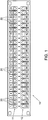
- a patch panel 10 may include a mother board (not shown) and a plurality of dual-connector units mountable on the mother board.
- the front end of patch panel 10 include an upper plurality of female modular conductive connectors (jacks) 20 arranged in an upper row 11 and a lower row 12 such that each jack within row 11 is a mirror image of a respective jack within lower row 12.
- Each dual-connector unit comprises a first jack on an upper row, a second jack on the lower row and an internal connecting conductive element (not shown) that electrically connect the pair of jacks.
- Each of jacks 20 may be typically terminated with a punch down type connector, such as IDC, positioned on the rear side of patch panel 10.
- IDC allows for termination of individual conductor wires to a certain jack. Each conductor wire may be correctly positioned and terminated to the correct IDC on the correct jack by a human installer. The individual conductor wires may be connected to any desired termination. Wires or cables, e.g., unshielded twisted pair (UTP) cables coupled to endpoint devices may be connected for example to the insulation displacement connectors (IDC's), positioned at the rear side of patch panel 10 (not shown). Patch panel 10 may be one of a plurality of patch panels mounted on the same communication rack.
- jacks 20 may be arranged in an upper row 11 and a lower row 12 positioned, such that the conductive contact jacks within row 11 are positioned in a mirror image relative to the contact jacks of lower row 12. Any other number of rows and any other structure of jacks, however, may be used.
- embodiments of the invention may include a plurality of patch panels which may include one or more rows of jacks.
- a first jack located at an upper row and a second jack located under the first jack at a lower row may be internally electrically connected without using any cord or cable.
- the electrical connection between jack no. 1 and jack no. 25, located below jack 1, may be established by an electrical element such as an electrical board or circuit as described in detail herein.
- the internal connection between pairs of jacks may provide cordless connections eliminating the use of patch cord cables to connect, for example, end users to network equipment.
- the assembly of the dual-connector unit includes two jacks and one conductive element with no external housing. Therefore, a number of N assemblies welded to a single motherboard may create a panel with 2*N jacks.
- the connecting element may be a conductive electrical circuit on the motherboard of the patch panel itself.
- the connecting elements may be a plurality of single elements.
- Such a patch panel may enable transfer of high data rates, e.g., higher than 500MHz due to the fact that at least one of the motherboard and the internal connecting element may include embedded cross-talk compensation elements.
- the exemplary patch panel 10 of Fig. 1 presents 24 assemblies of double connectors or double jacks according to embodiments of the present invention.
- jack no. 1 is connected to jack no. 25 as a first dual-connector
- jack no. 2 is connected to jack no. 26 as a second dual-connector
- jack no. 23 is connected to jack no. 47 as a twenty third dual-connector
- jack no. 24 is connected to jack no. 48 as a twenty fourth dual-connector.
- Any other connection of jacks which are not located one under the other may be established by using an external patch cord inserted into the relevant jacks. For example, upon insertion of a first end of a patch cord to jack no. 20, jack no. 20 would be disconnected from jack no. 44. Upon insertion of the second end of the patch cord to jack no. 31, jack no. 31 would be disconnected from jack no. 7 and be connected to jack no. 20.
- patch panel 10 and the connectors or jacks described herein may provide the basic characteristics of a structured cabling system according to international standards for structured cabling systems such as standards of the American National Standards Institute(ANSI), Telecommunications Industry Association (TIA), Electronic Industries Alliance (EIA) and International Organization for Standardization (ISO)/ International Electrotechnical Commission (IEC).
- ANSI American National Standards Institute
- TIA Telecommunications Industry Association
- EIA Electronic Industries Alliance
- ISO International Organization for Standardization
- ISO International Electrotechnical Commission
- IEC International Electrotechnical Commission
- the connectors described herein may include any type of connectors such as RJ45 at any performance levels such as, for example category 5, 5e, 6, 6A and higher, defined in these standards, copper connectors, fiber optics connectors, BNC connectors and others.
- the invention is not limited to such connectors, but is equally applicable to other known or subsequently developed connectors.
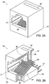
- Fig. 2A is a perspective view of a connector according to embodiments of the present invention
- Fig. 2B is a cross sectional view of a connector according to embodiments of the present invention.
- Connector 20 may include a housing 25 having a first opening or receiving cavity 21 and a second opening, slot or receiving cavity 22.
- the first receiving cavity 21 is to receive a communication plug, for example, a standard plug of a patch cord which may connect connector 20 to another connector and thereby connect between two communication ports.
- the second receiving cavity or slot 22 is to receive a conductive element or a connecting element (shown in Fig. 3 ) to electrically connect connector 20 to a second, substantially similar, connector.
- Slot 22 is located at the rear side of the connector's housing and it may be defined between an external rear wall 37 of housing 25 and an internal rear wall 38 of housing 25.
- Connector 20 may include an array of elongated, electrical, resilient conductive contacts or pins 24 for receiving electrical signals.
- the resilient conductive pins or electrical contacts 24 may be parallel and may be closely spaced such as to fit to an array of electrical contacts of a plug inserted into receiving cavity 21.
- Each electrical contact of electrical contacts 24 may include a first end extending through housing 25 as pins 27, a bend or a curved shape at its middle 26 and a resilient end at its second end 25, the resilient end may be located at slot 22.
- Resilient conductive pins 24 may be bent such that the first end of the resilient conductive pins may extend through and beyond external rear wall 37 and the second end of the resilient conductive pins may be positioned within slot 22, between external rear wall 37 and internal rear wall 38 without extending beyond external rear wall 37.
- Connector 20 may further include a support element 39 that may hold bent resilient conductive pins 24 such that a first portion of the resilient conducting pins 24 may be positioned between a surface of the housing and a bottom surface of the support element and a second portion of the bent resilient conductive pins 24 may be positioned over a top surface of the support element and does not extend beyond the rear wall 37.
- the resilient end 28 of resilient conductive pins 24 may be pushed down towards the bottom of connector 20 such as to allow an electrical contact.
- An electrical signal may progress from the electrical contacts of the inserted plug to electrical contacts 24 and from pins 27 to an external destination via, for example, an IDC block terminated on the rear side of a patch panel.
- a conductive element inserted into slot 22 may be in direct access and contact with resilient end 28 of the plurality of conductive contacts 24 inside connector 20 such as to electrically connect modular connector 20 to a substantially similar, modular connector.
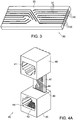
- Fig. 3 is a perspective view of a conductive electric circuit according to embodiments of the present invention.
- a conductive electric circuit or a conductive connecting element 30 may be used to electrically connect between two modular connectors or modular jacks such as connector 20 of Fig. 2A .
- conductive electric circuit 30 may include conductive pathways, tracks or signal traces 31 along its non- conductive body 33 and conductive contacts 32 at both top and bottom (not shown) ends of circuit 30.
- the number of conductive contacts 32 may be identical to the number of conductive contacts 24 inside connector 20 or may fit in any other way to conductive contacts 24 as to allow an electrical connection.
- Internal rear wall 38 may include a plurality of openings 36, e.g., the same number as the number of conductive pins 24, to allow the resilient conductive pins 24 to pass through or slide down through internal rear wall 38 while moving away from connecting element 30 when a plug is inserted into receiving cavity 21.
- Conductive connecting element 30 may be a printed circuit board (PCB), however any other electric circuit in any form or shape that may fit into the second opening 22 of connector 20 as to enable electrical connection between two connectors as described in the present invention may be used.
- Non-conductive body 33 may be formed of any suitable material, such as plastic or other suitable non-conductive material.
- Conductive signal traces 31 and conductive contacts 32 may be formed of a suitable material, such as metal. However, any suitable conductive material may be used.
- Connecting element 30 may include one or more cross-talk compensation elements which may be embedded into, mounted on or fixed to connecting element 30 in any method or technique in order to reduce or eliminate cross talk effects
- Fig. 4A is a perspective view of a dual connector assembly according to embodiments of the present invention
- Fig. 4B is a cross sectional view of a dual connector assembly according to embodiments of the present invention.
- a dual connector assembly 40 may include a first connector 45, a second connector 46 and a conductive element 47 to electrically connect the first connector to the second connector when inserted into a dedicated opening at both connectors as described herein.
- Connector 46 and connector 45 may be identical modular connectors and while being connected by conductive element 47, they may be organized in top-to-top arrangement, namely the upper part of connector 45 is directed to the upper part of connector 46 as shown in Fig.4A .
- Connector 45 may include a first opening 48 to receive a communication plug and a second opening 49 to receive a first end 71 of conductive element 47.
- Connector 46 may include a first opening 41 to receive a communication plug and a second opening 42 to receive a second end 72 of conductive element 47.
- an electrical contact may be made between the resilient ends 73 of the electrical contacts 43 and traces 44 of conductive element 47 via contacts at the top and bottom of conductive element 47 (contacts 32 shown in Fig. 3 ).
- an electrical connectivity may be made between pins 36 of connector 46 and pins 35 of connector 45 as to allow a high data transfer rate between connectors 45 and connector 46.
- a connection between connector 45 and connector 46 by conductive element 47 may allow a switch-less or a cable-less connection, namely, a connection made without any external wire or cable inserted in the standard openings of the connectors.
- a cable-less connection may enable transfer of a high data rates due to the fact that both conductive element 47 and the motherboard which connectors 45 and 46 are mounted to, for example, the patch panel (not shown) may have compensation elements.
- Fig. 5A is a cross sectional side view of a dual connector assembly 50 which may be connected or attached to motherboard 51 and termination blocks 52 and 53.
- motherboard 51 may be a patch panel motherboard, for example, path panel 10 of Fig. 1 .
- Dual connector assembly 50 may include a first modular jack or connector 55, a second modular jack or connector 56 and a conductive element 57.
- termination blocks 52 and 53 may be electrically connected via conductive traces of conductive element 57.
- a RJ45 connector may be plugged into termination block 53 and may be routed to a communication switch, while a horizontal cable may be connected to termination block 52 and routed to a personal computer.
- the personal computer may be constantly connected to the switch without the use of any additional cord or cable to connect between connectors 55 and 56.
- Fig. 5B is a cross sectional side view of a dual connector assembly 50 and a plug 60.
- Plug 60 may be inserted into the receiving opening 61 of connector 56 or into the receiving opening 62 of connector 55.
- an electrical connection may exist between termination block 52 and termination block 53 via connector 55, conductive element 57 and connector 56.
- plug 60 is inserted into a receiving opening of a connector, for example, receiving openings 62, the resilient part 63 of electrical contacts 64 may move away from conductive element 57 and the electrical connection between connector 55 and connector 56 may be disconnected.
- the resilient part 63 of electrical contacts 64 may move away from the electrical contacts on the bottom (or upper) side of the conductive element (Shown as contacts 32 in Fig. 3 ) as to eliminate the electrical connection between conductive element 57 and connector 55.
- the resilient conductive pins 24 are bend such that the second end of the resilient conductive pins 28 may move away from connecting element 57 by moving along the plurality of openings of the internal rear wall of the housing (openings 36 of Fig. 2B ).
- Embodiments of the invention may allow a standard use of connectors 55 and 56 if a plug is inserted into at least one of them, as a plug insertion may disable the electrical connection between connectors 55 and 56 via conductive element 57. However, if no plug is inserted into connector 55 and no plug is inserted into connector 56, conductive element 57 may connect connector 55 and connector 56 such as to enable an electrical connection between termination block 52 and termination block 53 without any use of a cable, cord or external connection between connector 55 and connector 56.
Landscapes
- Engineering & Computer Science (AREA)
- Microelectronics & Electronic Packaging (AREA)
- Details Of Connecting Devices For Male And Female Coupling (AREA)
- Coupling Device And Connection With Printed Circuit (AREA)
Claims (14)
- Connecteur jack (20) pouvant être monté sur un panneau de brassage comprenant :un boîtier (25) ayant une seule cavité de réception (21) configurée pour recevoir une fiche de communication d'un standard connu etdes broches conductrices élastiques (24) pliées de sorte qu'une première extrémité des broches conductrices élastiques s'étend à travers et au-delà de la paroi arrière externe du boîtier, une seconde extrémité des broches conductrices élastiques étant positionnée entre la paroi arrière externe du boîtier et la paroi arrière interne du boîtier,caractérisé en ce que le boîtier comprend en outre une fente (22), la fente étant définie entre une paroi arrière externe (37) du boîtier et une paroi arrière interne (38) du boîtier; etdans lequel la fente est configurée pour recevoir une première extrémité d'un élément de connexion, de sorte que les broches conductrices élastiques (24) sont électriquement connectées aux contacts de l'élément de connexion et, lorsqu'une fiche de communication est insérée dans la cavité de réception, les broches conductrices élastiques s'écartent de l'élément de connexion.
- Unité à double connecteur (40) comprenant :un premier connecteur jack (45, 55) selon la revendication 1;un second connecteur jack (46, 56) selon la revendication 1; etun élément de connexion (30, 47, 57) ayant une première pluralité de contacts (32) sur une première extrémité (71) de l'élément de connexion (47) et une seconde pluralité de contacts (32) sur une seconde extrémité (72) de l'élément de connexion (47), l'élément de connexion étant configuré pour fournir une connexion électrique entre les premier et second connecteurs jack (45, 46),dans lequel la fente (22, 49) du boîtier du premier connecteur jack est configurée pour recevoir la première extrémité (71) de l'élément de connexion (47),dans lequel la fente (22, 42) du boîtier du deuxième connecteur jack est configurée pour recevoir la deuxième extrémité (71) de l'élément de connexion (47),dans lequel le la première extrémité (71) de l'élément de connexion (47) se trouve dans la fente (49) du boîtier du premier connecteur jack pour connecter électriquement la pluralité de broches conductrices élastiques du premier connecteur jack et la pluralité de contacts du premier jack connecteur sur une première extrémité (71) de l'élément de connexion (47), et la seconde extrémité (72) du l'élément de connexion (47) se trouve dans la fente (42) du boîtier du deuxième connecteur jack pour connecter électriquement la pluralité de broches conductrices élastiques du deuxième connecteur jack et la pluralité de contacts du deuxième connecteur jack sur une deuxième extrémité (72) de l'élément de connexion (47),de sorte que, lorsqu'une fiche de communication est insérée dans la cavité de réception du premier ou du deuxième connecteur jack, la pluralité de broches conductrices élastiques du premier ou deuxième connecteur jack respectif s'écarte de l'élément de connexion (47).
- Unité à double connecteur (40) selon la revendication 2, dans laquelle l'unité à double connecteur est soudée à une carte mère d'un panneau de brassage.
- Unité à double connecteur selon la revendication 2, dans laquelle l'élément de connexion (47) comprend une carte de circuit imprimé conductrice.
- Unité à double connecteur selon la revendication 2, dans laquelle l'élément de connexion comprend un élément de compensation.
- Unité à double connecteur selon la revendication 2, dans laquelle le premier connecteur jack fait partie d'une rangée supérieure (11) d'un panneau de brassage (10) et le second connecteur jack fait partie d'une rangée inférieure (12) du panneau de brassage (10).
- Unité à double connecteur selon la revendication 2, dans laquelle la paroi arrière interne (38) de chacun des premier et second boîtiers comprend une pluralité d'ouvertures (36) pour permettre aux broches conductrices élastiques de traverser la paroi arrière interne du boîtier tout en s'écartant de l'élément de connexion lorsque la fiche de communication est insérée dans la cavité de réception.
- Unité à double connecteur selon la revendication 7, dans laquelle, lorsque la fiche de communication est insérée dans la cavité de réception, les broches conductrices élastiques sont pliées de sorte que la seconde extrémité des broches conductrices élastiques s'écarte de l'élément de connexion en se déplaçant le long de la pluralité d'ouvertures de la paroi arrière interne du boîtier.
- Panneau de brassage comprenant :une carte mère (51); etune pluralité d'unités à double connecteur (50) selon l'une quelconque des revendications 2 à 8, soudées à la carte mère (51).
- Panneau de brassage selon la revendication 9, dans lequel le premier connecteur jack de chaque double connecteur fait partie d'une rangée supérieure (11) du panneau de brassage (10) et le deuxième connecteur jack de chaque double connecteur fait partie d'une rangée inférieure (12) du panneau de brassage (10).
- Panneau de brassage selon la revendication 9, dans lequel la carte mère (51) comprend un élément de compensation.
- Panneau de brassage selon la revendication 9, dans lequel l'élément de connexion (57) comprend une carte de circuit imprimé conductrice.
- Panneau de brassage selon la revendication 9 ou la revendication 12, dans lequel l'élément de connexion comprend un élément de compensation.
- Panneau de brassage selon la revendication 9, dans lequel la paroi arrière interne de chacun des premier et second boîtiers comprend une pluralité d'ouvertures pour permettre aux broches conductrices élastiques de traverser la paroi arrière interne du boîtier tout en s'écartant de l'élément de connexion lorsque la fiche de communication (60) est insérée dans la cavité de réception.
Applications Claiming Priority (2)
| Application Number | Priority Date | Filing Date | Title |
|---|---|---|---|
| US29291210P | 2010-01-07 | 2010-01-07 | |
| PCT/IL2011/000014 WO2011083470A1 (fr) | 2010-01-07 | 2011-01-06 | Connecteur modulaire pour dispositif de raccordement sans câble |
Publications (3)
| Publication Number | Publication Date |
|---|---|
| EP2522055A1 EP2522055A1 (fr) | 2012-11-14 |
| EP2522055A4 EP2522055A4 (fr) | 2014-07-09 |
| EP2522055B1 true EP2522055B1 (fr) | 2021-06-16 |
Family
ID=44305241
Family Applications (1)
| Application Number | Title | Priority Date | Filing Date |
|---|---|---|---|
| EP11731738.8A Active EP2522055B1 (fr) | 2010-01-07 | 2011-01-06 | Connecteur modulaire pour dispositif de raccordement sans câble |
Country Status (5)
| Country | Link |
|---|---|
| US (1) | US8851902B2 (fr) |
| EP (1) | EP2522055B1 (fr) |
| CN (1) | CN102754287B (fr) |
| BR (1) | BR112012016779A2 (fr) |
| WO (1) | WO2011083470A1 (fr) |
Families Citing this family (7)
| Publication number | Priority date | Publication date | Assignee | Title |
|---|---|---|---|---|
| AU2014202653A1 (en) * | 2013-05-20 | 2014-12-04 | IKONOMOU, Konstantinos MR | Patch Panel Arrangement, Cable Terminating Devices & Methods |
| CN110109854A (zh) * | 2013-08-29 | 2019-08-09 | 洛克波特网络股份有限公司 | 管理计算机网络的直接互连交换机布线与增长的方法和装置 |
| US9413097B2 (en) * | 2014-12-22 | 2016-08-09 | Intel Corporation | High density cabled midplanes and backplanes |
| US9832904B1 (en) * | 2016-03-28 | 2017-11-28 | Amazon Technologies, Inc. | Patch panel assembly |
| TWM539726U (zh) * | 2016-07-29 | 2017-04-11 | P-Two Ind Inc | 連接器組合結構 |
| DE102017003161A1 (de) * | 2017-03-31 | 2018-10-04 | Yamaichi Electronics Deutschland Gmbh | Steckkupplungsvorrichtung, Verfahren und Verwendung |
| RU2768362C1 (ru) * | 2021-02-12 | 2022-03-24 | Федеральное государственное бюджетное образовательное учреждение высшего образования "Национальный исследовательский Московский государственный строительный университет" (НИУ МГСУ) | Коммутационное поле физического уровня информационных IP-систем с централизованной структурой |
Family Cites Families (11)
| Publication number | Priority date | Publication date | Assignee | Title |
|---|---|---|---|---|
| US5178554A (en) | 1990-10-26 | 1993-01-12 | The Siemon Company | Modular jack patching device |
| US6012936A (en) | 1996-10-16 | 2000-01-11 | The Siemon Company | Switching jack |
| US6394850B1 (en) * | 2000-03-20 | 2002-05-28 | David Oliphant | Contact pin design for a modular jack |
| US6371780B1 (en) | 2000-05-15 | 2002-04-16 | Avaya Technology Corp. | RJ jack with switch |
| US6612856B1 (en) * | 2001-12-17 | 2003-09-02 | 3Com Corporation | Apparatus and methods for preventing cable-discharge damage to electronic equipment |
| US6644995B1 (en) * | 2002-08-05 | 2003-11-11 | Hon Hai Precision Ind. Co., Ltd. | Low insertion force electrical connector |
| CN2687899Y (zh) * | 2003-12-12 | 2005-03-23 | 富士康(昆山)电脑接插件有限公司 | 电连接器 |
| US7241181B2 (en) | 2004-06-29 | 2007-07-10 | Pulse Engineering, Inc. | Universal connector assembly and method of manufacturing |
| CN2831476Y (zh) * | 2005-08-17 | 2006-10-25 | 富士康(昆山)电脑接插件有限公司 | 模组连接器 |
| US7530854B2 (en) * | 2006-06-15 | 2009-05-12 | Ortronics, Inc. | Low noise multiport connector |
| US8147278B2 (en) * | 2007-03-01 | 2012-04-03 | Pulse Electronics, Inc. | Integrated connector apparatus and methods |
-
2011
- 2011-01-06 US US13/520,832 patent/US8851902B2/en active Active
- 2011-01-06 CN CN201180008634.6A patent/CN102754287B/zh active Active
- 2011-01-06 EP EP11731738.8A patent/EP2522055B1/fr active Active
- 2011-01-06 WO PCT/IL2011/000014 patent/WO2011083470A1/fr not_active Ceased
- 2011-01-06 BR BR112012016779-0A patent/BR112012016779A2/pt not_active Application Discontinuation
Non-Patent Citations (1)
| Title |
|---|
| None * |
Also Published As
| Publication number | Publication date |
|---|---|
| CN102754287B (zh) | 2015-04-01 |
| US8851902B2 (en) | 2014-10-07 |
| EP2522055A4 (fr) | 2014-07-09 |
| BR112012016779A2 (pt) | 2020-09-01 |
| US20130130516A1 (en) | 2013-05-23 |
| CN102754287A (zh) | 2012-10-24 |
| WO2011083470A1 (fr) | 2011-07-14 |
| EP2522055A1 (fr) | 2012-11-14 |
Similar Documents
| Publication | Publication Date | Title |
|---|---|---|
| US7503810B1 (en) | Board edge termination back-end connection assemblies and communications jacks including such assemblies | |
| US8758047B2 (en) | Port replication assembly with adapter cable and related methods of use | |
| US7857635B2 (en) | Board edge termination back-end connection assemblies and communications connectors including such assemblies | |
| US8882514B2 (en) | Datacommunications modules, cable-connector assemblies and components therefor | |
| US8398441B2 (en) | Assembly and system of datacommunication cables and connectors | |
| US9876322B2 (en) | Backward compatible connectivity for high data rate applications | |
| EP2522055B1 (fr) | Connecteur modulaire pour dispositif de raccordement sans câble | |
| CN110350334A (zh) | 电互连系统 | |
| US6358093B1 (en) | Normal through jack and method | |
| US6945820B1 (en) | Electrical connect having integrated over current protector | |
| US10153592B2 (en) | Communications connectors | |
| CN101167004A (zh) | 双工插头适配器模块 | |
| CN107925199B (zh) | Rj45插头 | |
| EP1171933B1 (fr) | Connecteur a cordon de connexion | |
| GB2437157A (en) | Electrical connector having shielding around each contact |
Legal Events
| Date | Code | Title | Description |
|---|---|---|---|
| PUAI | Public reference made under article 153(3) epc to a published international application that has entered the european phase |
Free format text: ORIGINAL CODE: 0009012 |
|
| 17P | Request for examination filed |
Effective date: 20120716 |
|
| AK | Designated contracting states |
Kind code of ref document: A1 Designated state(s): AL AT BE BG CH CY CZ DE DK EE ES FI FR GB GR HR HU IE IS IT LI LT LU LV MC MK MT NL NO PL PT RO RS SE SI SK SM TR |
|
| DAX | Request for extension of the european patent (deleted) | ||
| A4 | Supplementary search report drawn up and despatched |
Effective date: 20140612 |
|
| RIC1 | Information provided on ipc code assigned before grant |
Ipc: H01R 13/60 20060101AFI20140605BHEP Ipc: H01R 12/71 20110101ALI20140605BHEP Ipc: H01R 13/703 20060101ALI20140605BHEP Ipc: H01R 31/06 20060101ALI20140605BHEP Ipc: H01R 24/64 20110101ALI20140605BHEP Ipc: H01R 13/66 20060101ALI20140605BHEP Ipc: H01R 24/00 20110101ALI20140605BHEP |
|
| STAA | Information on the status of an ep patent application or granted ep patent |
Free format text: STATUS: REQUEST FOR EXAMINATION WAS MADE |
|
| 19U | Interruption of proceedings before grant |
Effective date: 20160705 |
|
| 19W | Proceedings resumed before grant after interruption of proceedings |
Effective date: 20190701 |
|
| RAP1 | Party data changed (applicant data changed or rights of an application transferred) |
Owner name: RIT TECH (INTELLIGENCE SOLUTIONS) LTD. |
|
| STAA | Information on the status of an ep patent application or granted ep patent |
Free format text: STATUS: EXAMINATION IS IN PROGRESS |
|
| 17Q | First examination report despatched |
Effective date: 20191018 |
|
| GRAP | Despatch of communication of intention to grant a patent |
Free format text: ORIGINAL CODE: EPIDOSNIGR1 |
|
| STAA | Information on the status of an ep patent application or granted ep patent |
Free format text: STATUS: GRANT OF PATENT IS INTENDED |
|
| INTG | Intention to grant announced |
Effective date: 20201222 |
|
| GRAS | Grant fee paid |
Free format text: ORIGINAL CODE: EPIDOSNIGR3 |
|
| GRAA | (expected) grant |
Free format text: ORIGINAL CODE: 0009210 |
|
| STAA | Information on the status of an ep patent application or granted ep patent |
Free format text: STATUS: THE PATENT HAS BEEN GRANTED |
|
| AK | Designated contracting states |
Kind code of ref document: B1 Designated state(s): AL AT BE BG CH CY CZ DE DK EE ES FI FR GB GR HR HU IE IS IT LI LT LU LV MC MK MT NL NO PL PT RO RS SE SI SK SM TR |
|
| REG | Reference to a national code |
Ref country code: GB Ref legal event code: FG4D |
|
| REG | Reference to a national code |
Ref country code: CH Ref legal event code: EP |
|
| REG | Reference to a national code |
Ref country code: DE Ref legal event code: R096 Ref document number: 602011071166 Country of ref document: DE |
|
| REG | Reference to a national code |
Ref country code: AT Ref legal event code: REF Ref document number: 1403112 Country of ref document: AT Kind code of ref document: T Effective date: 20210715 |
|
| REG | Reference to a national code |
Ref country code: IE Ref legal event code: FG4D |
|
| REG | Reference to a national code |
Ref country code: LT Ref legal event code: MG9D |
|
| PG25 | Lapsed in a contracting state [announced via postgrant information from national office to epo] |
Ref country code: BG Free format text: LAPSE BECAUSE OF FAILURE TO SUBMIT A TRANSLATION OF THE DESCRIPTION OR TO PAY THE FEE WITHIN THE PRESCRIBED TIME-LIMIT Effective date: 20210916 Ref country code: HR Free format text: LAPSE BECAUSE OF FAILURE TO SUBMIT A TRANSLATION OF THE DESCRIPTION OR TO PAY THE FEE WITHIN THE PRESCRIBED TIME-LIMIT Effective date: 20210616 Ref country code: LT Free format text: LAPSE BECAUSE OF FAILURE TO SUBMIT A TRANSLATION OF THE DESCRIPTION OR TO PAY THE FEE WITHIN THE PRESCRIBED TIME-LIMIT Effective date: 20210616 Ref country code: FI Free format text: LAPSE BECAUSE OF FAILURE TO SUBMIT A TRANSLATION OF THE DESCRIPTION OR TO PAY THE FEE WITHIN THE PRESCRIBED TIME-LIMIT Effective date: 20210616 |
|
| REG | Reference to a national code |
Ref country code: AT Ref legal event code: MK05 Ref document number: 1403112 Country of ref document: AT Kind code of ref document: T Effective date: 20210616 |
|
| REG | Reference to a national code |
Ref country code: NL Ref legal event code: MP Effective date: 20210616 |
|
| PG25 | Lapsed in a contracting state [announced via postgrant information from national office to epo] |
Ref country code: NO Free format text: LAPSE BECAUSE OF FAILURE TO SUBMIT A TRANSLATION OF THE DESCRIPTION OR TO PAY THE FEE WITHIN THE PRESCRIBED TIME-LIMIT Effective date: 20210916 Ref country code: RS Free format text: LAPSE BECAUSE OF FAILURE TO SUBMIT A TRANSLATION OF THE DESCRIPTION OR TO PAY THE FEE WITHIN THE PRESCRIBED TIME-LIMIT Effective date: 20210616 Ref country code: SE Free format text: LAPSE BECAUSE OF FAILURE TO SUBMIT A TRANSLATION OF THE DESCRIPTION OR TO PAY THE FEE WITHIN THE PRESCRIBED TIME-LIMIT Effective date: 20210616 Ref country code: GR Free format text: LAPSE BECAUSE OF FAILURE TO SUBMIT A TRANSLATION OF THE DESCRIPTION OR TO PAY THE FEE WITHIN THE PRESCRIBED TIME-LIMIT Effective date: 20210917 Ref country code: LV Free format text: LAPSE BECAUSE OF FAILURE TO SUBMIT A TRANSLATION OF THE DESCRIPTION OR TO PAY THE FEE WITHIN THE PRESCRIBED TIME-LIMIT Effective date: 20210616 |
|
| PG25 | Lapsed in a contracting state [announced via postgrant information from national office to epo] |
Ref country code: CZ Free format text: LAPSE BECAUSE OF FAILURE TO SUBMIT A TRANSLATION OF THE DESCRIPTION OR TO PAY THE FEE WITHIN THE PRESCRIBED TIME-LIMIT Effective date: 20210616 Ref country code: EE Free format text: LAPSE BECAUSE OF FAILURE TO SUBMIT A TRANSLATION OF THE DESCRIPTION OR TO PAY THE FEE WITHIN THE PRESCRIBED TIME-LIMIT Effective date: 20210616 Ref country code: SM Free format text: LAPSE BECAUSE OF FAILURE TO SUBMIT A TRANSLATION OF THE DESCRIPTION OR TO PAY THE FEE WITHIN THE PRESCRIBED TIME-LIMIT Effective date: 20210616 Ref country code: SK Free format text: LAPSE BECAUSE OF FAILURE TO SUBMIT A TRANSLATION OF THE DESCRIPTION OR TO PAY THE FEE WITHIN THE PRESCRIBED TIME-LIMIT Effective date: 20210616 Ref country code: AT Free format text: LAPSE BECAUSE OF FAILURE TO SUBMIT A TRANSLATION OF THE DESCRIPTION OR TO PAY THE FEE WITHIN THE PRESCRIBED TIME-LIMIT Effective date: 20210616 Ref country code: PT Free format text: LAPSE BECAUSE OF FAILURE TO SUBMIT A TRANSLATION OF THE DESCRIPTION OR TO PAY THE FEE WITHIN THE PRESCRIBED TIME-LIMIT Effective date: 20211018 Ref country code: NL Free format text: LAPSE BECAUSE OF FAILURE TO SUBMIT A TRANSLATION OF THE DESCRIPTION OR TO PAY THE FEE WITHIN THE PRESCRIBED TIME-LIMIT Effective date: 20210616 Ref country code: RO Free format text: LAPSE BECAUSE OF FAILURE TO SUBMIT A TRANSLATION OF THE DESCRIPTION OR TO PAY THE FEE WITHIN THE PRESCRIBED TIME-LIMIT Effective date: 20210616 Ref country code: ES Free format text: LAPSE BECAUSE OF FAILURE TO SUBMIT A TRANSLATION OF THE DESCRIPTION OR TO PAY THE FEE WITHIN THE PRESCRIBED TIME-LIMIT Effective date: 20210616 |
|
| PG25 | Lapsed in a contracting state [announced via postgrant information from national office to epo] |
Ref country code: PL Free format text: LAPSE BECAUSE OF FAILURE TO SUBMIT A TRANSLATION OF THE DESCRIPTION OR TO PAY THE FEE WITHIN THE PRESCRIBED TIME-LIMIT Effective date: 20210616 |
|
| REG | Reference to a national code |
Ref country code: DE Ref legal event code: R097 Ref document number: 602011071166 Country of ref document: DE |
|
| PLBE | No opposition filed within time limit |
Free format text: ORIGINAL CODE: 0009261 |
|
| STAA | Information on the status of an ep patent application or granted ep patent |
Free format text: STATUS: NO OPPOSITION FILED WITHIN TIME LIMIT |
|
| PG25 | Lapsed in a contracting state [announced via postgrant information from national office to epo] |
Ref country code: DK Free format text: LAPSE BECAUSE OF FAILURE TO SUBMIT A TRANSLATION OF THE DESCRIPTION OR TO PAY THE FEE WITHIN THE PRESCRIBED TIME-LIMIT Effective date: 20210616 |
|
| 26N | No opposition filed |
Effective date: 20220317 |
|
| PG25 | Lapsed in a contracting state [announced via postgrant information from national office to epo] |
Ref country code: AL Free format text: LAPSE BECAUSE OF FAILURE TO SUBMIT A TRANSLATION OF THE DESCRIPTION OR TO PAY THE FEE WITHIN THE PRESCRIBED TIME-LIMIT Effective date: 20210616 |
|
| PG25 | Lapsed in a contracting state [announced via postgrant information from national office to epo] |
Ref country code: IT Free format text: LAPSE BECAUSE OF FAILURE TO SUBMIT A TRANSLATION OF THE DESCRIPTION OR TO PAY THE FEE WITHIN THE PRESCRIBED TIME-LIMIT Effective date: 20210616 |
|
| PG25 | Lapsed in a contracting state [announced via postgrant information from national office to epo] |
Ref country code: MC Free format text: LAPSE BECAUSE OF FAILURE TO SUBMIT A TRANSLATION OF THE DESCRIPTION OR TO PAY THE FEE WITHIN THE PRESCRIBED TIME-LIMIT Effective date: 20210616 |
|
| REG | Reference to a national code |
Ref country code: CH Ref legal event code: PL |
|
| REG | Reference to a national code |
Ref country code: BE Ref legal event code: MM Effective date: 20220131 |
|
| PG25 | Lapsed in a contracting state [announced via postgrant information from national office to epo] |
Ref country code: LU Free format text: LAPSE BECAUSE OF NON-PAYMENT OF DUE FEES Effective date: 20220106 |
|
| PG25 | Lapsed in a contracting state [announced via postgrant information from national office to epo] |
Ref country code: BE Free format text: LAPSE BECAUSE OF NON-PAYMENT OF DUE FEES Effective date: 20220131 |
|
| PG25 | Lapsed in a contracting state [announced via postgrant information from national office to epo] |
Ref country code: LI Free format text: LAPSE BECAUSE OF NON-PAYMENT OF DUE FEES Effective date: 20220131 Ref country code: CH Free format text: LAPSE BECAUSE OF NON-PAYMENT OF DUE FEES Effective date: 20220131 |
|
| PG25 | Lapsed in a contracting state [announced via postgrant information from national office to epo] |
Ref country code: IE Free format text: LAPSE BECAUSE OF NON-PAYMENT OF DUE FEES Effective date: 20220106 |
|
| P01 | Opt-out of the competence of the unified patent court (upc) registered |
Effective date: 20230608 |
|
| PG25 | Lapsed in a contracting state [announced via postgrant information from national office to epo] |
Ref country code: HU Free format text: LAPSE BECAUSE OF FAILURE TO SUBMIT A TRANSLATION OF THE DESCRIPTION OR TO PAY THE FEE WITHIN THE PRESCRIBED TIME-LIMIT; INVALID AB INITIO Effective date: 20110106 |
|
| PG25 | Lapsed in a contracting state [announced via postgrant information from national office to epo] |
Ref country code: MK Free format text: LAPSE BECAUSE OF FAILURE TO SUBMIT A TRANSLATION OF THE DESCRIPTION OR TO PAY THE FEE WITHIN THE PRESCRIBED TIME-LIMIT Effective date: 20210616 Ref country code: CY Free format text: LAPSE BECAUSE OF FAILURE TO SUBMIT A TRANSLATION OF THE DESCRIPTION OR TO PAY THE FEE WITHIN THE PRESCRIBED TIME-LIMIT Effective date: 20210616 |
|
| PG25 | Lapsed in a contracting state [announced via postgrant information from national office to epo] |
Ref country code: TR Free format text: LAPSE BECAUSE OF FAILURE TO SUBMIT A TRANSLATION OF THE DESCRIPTION OR TO PAY THE FEE WITHIN THE PRESCRIBED TIME-LIMIT Effective date: 20210616 |
|
| PG25 | Lapsed in a contracting state [announced via postgrant information from national office to epo] |
Ref country code: MT Free format text: LAPSE BECAUSE OF FAILURE TO SUBMIT A TRANSLATION OF THE DESCRIPTION OR TO PAY THE FEE WITHIN THE PRESCRIBED TIME-LIMIT Effective date: 20210616 |
|
| PGFP | Annual fee paid to national office [announced via postgrant information from national office to epo] |
Ref country code: GB Payment date: 20251223 Year of fee payment: 16 |
|
| PGFP | Annual fee paid to national office [announced via postgrant information from national office to epo] |
Ref country code: DE Payment date: 20251229 Year of fee payment: 16 |
|
| PGFP | Annual fee paid to national office [announced via postgrant information from national office to epo] |
Ref country code: FR Payment date: 20260126 Year of fee payment: 16 |