EP2523531A1 - Verfahren und Vorrichtung zur Ansteuerung einer Leuchtdiode - Google Patents
Verfahren und Vorrichtung zur Ansteuerung einer Leuchtdiode Download PDFInfo
- Publication number
- EP2523531A1 EP2523531A1 EP11003782A EP11003782A EP2523531A1 EP 2523531 A1 EP2523531 A1 EP 2523531A1 EP 11003782 A EP11003782 A EP 11003782A EP 11003782 A EP11003782 A EP 11003782A EP 2523531 A1 EP2523531 A1 EP 2523531A1
- Authority
- EP
- European Patent Office
- Prior art keywords
- current
- terminal
- led modules
- control circuits
- guiding control
- Prior art date
- Legal status (The legal status is an assumption and is not a legal conclusion. Google has not performed a legal analysis and makes no representation as to the accuracy of the status listed.)
- Withdrawn
Links
- 238000000034 method Methods 0.000 title claims abstract description 13
- 230000001965 increasing effect Effects 0.000 claims description 4
- 230000003247 decreasing effect Effects 0.000 claims description 3
- 238000011144 upstream manufacturing Methods 0.000 claims description 3
- 238000010586 diagram Methods 0.000 description 8
- 238000001514 detection method Methods 0.000 description 5
- 239000003990 capacitor Substances 0.000 description 4
- WFKWXMTUELFFGS-UHFFFAOYSA-N tungsten Chemical compound [W] WFKWXMTUELFFGS-UHFFFAOYSA-N 0.000 description 3
- 229910052721 tungsten Inorganic materials 0.000 description 3
- 239000010937 tungsten Substances 0.000 description 3
- 230000000694 effects Effects 0.000 description 2
- 238000005286 illumination Methods 0.000 description 2
- 229920006395 saturated elastomer Polymers 0.000 description 2
- 238000010276 construction Methods 0.000 description 1
- 230000008878 coupling Effects 0.000 description 1
- 238000010168 coupling process Methods 0.000 description 1
- 238000005859 coupling reaction Methods 0.000 description 1
- 238000001035 drying Methods 0.000 description 1
- 230000005611 electricity Effects 0.000 description 1
- 238000005516 engineering process Methods 0.000 description 1
- 238000001914 filtration Methods 0.000 description 1
- 230000020169 heat generation Effects 0.000 description 1
- 230000001939 inductive effect Effects 0.000 description 1
- 230000007257 malfunction Effects 0.000 description 1
- 238000004519 manufacturing process Methods 0.000 description 1
- 238000012986 modification Methods 0.000 description 1
- 230000004048 modification Effects 0.000 description 1
- 239000004065 semiconductor Substances 0.000 description 1
- 230000000087 stabilizing effect Effects 0.000 description 1
- 230000001131 transforming effect Effects 0.000 description 1
- 239000002918 waste heat Substances 0.000 description 1
Images


Classifications
-
- H—ELECTRICITY
- H05—ELECTRIC TECHNIQUES NOT OTHERWISE PROVIDED FOR
- H05B—ELECTRIC HEATING; ELECTRIC LIGHT SOURCES NOT OTHERWISE PROVIDED FOR; CIRCUIT ARRANGEMENTS FOR ELECTRIC LIGHT SOURCES, IN GENERAL
- H05B45/00—Circuit arrangements for operating light-emitting diodes [LED]
- H05B45/40—Details of LED load circuits
- H05B45/44—Details of LED load circuits with an active control inside an LED matrix
- H05B45/48—Details of LED load circuits with an active control inside an LED matrix having LEDs organised in strings and incorporating parallel shunting devices
Definitions
- the present invention relates to a driving method, and more particularly, to a method and device for driving a light-emitting diode (LED) with an improved power factor and power utilization efficiency and a reduced electromagnetic interference.
- LED light-emitting diode
- LEDs are advantageous in long service life, low power consumption and low waste heat generation. All of these advantages promote the development of LED lighting equipments.
- An LED is normally driven by a DC power source.
- an AC power source such as a mains electricity supply
- it has to be provided with an LED driver circuit that converts the incoming AC power into a pulsed DC power, so that the LED can emit light upon receipt of the DC power.
- a conventional LED driver circuit 100 is connected to at least one LED 101 and adapted to receive an AC power VAC.
- the LED driver circuit 100 mainly comprises a bridge rectifier 110 and a capacitor C.
- the bridge rectifier 110 is used to rectify the AC power VAC into a pulsed DC power, and then the capacitor C stabilizes the voltage of the pulsed DC power for driving the LED 101 to emit light.
- a constant current circuit is further provided to maintain the current at a constant level, thereby stabilizing the brightness and chromaticity of the light emission from the LED.
- An inductive reactance element such as a capacitor or an inductor, if present in the circuit, will make the voltage and current out of phase by a phase difference ( ⁇ ), as shown in FIG. 4(C) .
- PF(Power Factor) V(Voltage) ⁇ I (Current) ⁇ cos ⁇
- the presence of the phase difference ( ⁇ ) causes a decrease in power factor which in turn results in an increase in power loss.
- R.O.C. Patent No. 1220047 entitled “LED Driver Circuit,” discloses an LED driver circuit as shown in FIG. 5 , which includes a power source 51, multiple current guiding control circuits 52 composed of one or more common-ground current control units 521, and a voltage detection circuit 53 for detecting the voltage level of the supplied power.
- the power source 51 is connected in series to one or more LED sets 54, each being composed of one or more LEDs.
- the current control units 521 of the current guiding control circuits 52 are sequentially connected to the N-electrodes (negative electrodes) of the respective LED sets 54.
- the voltage level of the positive part of the supplied power is detected by the voltage detection circuit 53.
- one of the current guiding control circuits 52 is selectively placed in a conductive state according to the voltage level, whereby a suitable amount of the LED sets 54 are driven to emit light.
- a circuit design allows the voltage of the positive part of the supplied power to directly drive the LED sets, so that a maximum number of LED sets are driven to emit light according to the voltage level without coupling to a filtering capacitor, thereby achieving the purposes of efficiently utilizing electric power, increasing power factor and reducing power loss.
- an object of the invention is to provide a driving method, and more particularly, to a method and device for driving a light-emitting diode (LED) directly by AC mains power without switching the frequency, thereby achieving the purposes of improving power factor and reducing power loss and electromagnetic interference.
- LED light-emitting diode
- the inventive driving method comprises using a plurality of current guiding control circuits to drive a plurality of LED modules, wherein each of the current guiding control circuits includes at least two transistors connected in parallel to constitute at least two switch circuits.
- Each of the respective current guiding control circuits is adapted to permit or prevent electric current to flow to an immediate downstream one of the LED modules in response to a predetermined voltage level of the positive part of a voltage source.
- the respective current guiding control circuits are responsive to different voltage levels. As a result, a maximum number of LED modules are driven to emit light at a given voltage level, thereby achieving the purposes of efficiently utilizing electric power and reducing power loss.
- the present invention provides a method for driving a light-emitting diode.
- the method comprises using a plurality of current guiding control circuits to drive a plurality of LED modules, wherein each of current guiding control circuits includes at least two transistors connected to constitute at least two switch circuits, and wherein the respective current guiding control circuits differ from one another by their responses to different current levels of a voltage source, so that the respective LED modules under their control are selectively driven to emit light at different voltage levels.
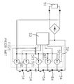
- the invention further provides a driver device as illustrated in FIG. 1 , which comprises the following constituting elements:
- Vs Voltage source
- the voltage source is provided with a rectifying circuit 40 (which may by way of example be a bridge rectifier), so that an alternating current (AC) power received from the voltage source is converted into a pulsed direct current (DC) voltage source, as shown in FIG. 3(A) .
- a rectifying circuit 40 which may by way of example be a bridge rectifier
- At least two LED modules are included in the inventive device. According to the embodiment illustrated in FIG. 1 , there are five LED modules 11, 12, 13, 14, 15 included in the device, each comprising single or multiple LEDs L connected in series, or in parallel, or in a combination of both. Preferably, the amount of the LEDs mounted in the respective LED modules are gradually increased and then decreased from the LED module 11 to the LED module 15.
- At least one current guiding control circuit is coupled between two adjacent LED modules.
- the first and second transistors 251, 252 are each provided with a first terminal, a second terminal and a control terminal.
- the first and second transistors 251, 252 are NPN-type bipolar junction transistors (BJT), in which the first terminal, the second terminal and the control terminal pertain to an emitter E, a collector C and a base B, respectively.
- BJT NPN-type bipolar junction transistors
- the first input terminal 255 is connected in parallel to a positive electrode of one of the LED modules 12, 13, 14, 15 and connected in series to a negative electrode of another one of the LED modules 11, 12, 13, 14 which is upstream of the one LED module.
- the second input terminal 256 is connected to the voltage source Vs for receiving the rectified power.
- the first input terminal 255 is connected to the emitter E at the first terminal of the first transistor 251.
- the base B at the control terminal of the first transistor 251 is connected to an end of the first resistor 253, while the other end of the first resistor 253 and the collector C at the first terminal of the second transistor 252 are connected via a common line to the second output terminal 256 where a third resistor 259 is mounted.
- the base B at the control terminal of the second transistor 252 is connected to an end of the second resistor 254, while the other end of the second resistor 254 and the emitter E at the second terminal of the first transistor 251 are connected via a common line to the first output terminal 257 which is in turn connected to the negative electrode of the LED module under its control.
- the emitter E at the second terminal of the second transistor 252 is coupled to the second output terminal 258 which is in turn connected to a positive electrode of another one of the LED modules 13, 14, 15 which is downstream of the one LED module.
- the fourth resistor 250 is coupled between the base B at the control terminal and the emitter E at the second terminal of the second transistor 252.
- a current source circuit 30 is coupled between the rectifying circuit 40 and the LED modules 11-15 and adapted to convert the pulsed DC voltage source into a pulsed DC current source in phase therewith.
- the current source circuit 30 provides a loop current to the respective LED modules 11-15 to achieve a satisfactory power factor.
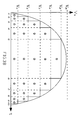
- FIG. 3(B) is a diagram showing the ON/OFF states of the respective LED modules within a half wave period of the supplied AC power.
- the first LED module 11 receives sufficient electric current and starts to emit light when the voltage of the power source reaches a level of Vs1.
- the second transistor 252 in the first current guiding control circuit is operated in its cut-off region and switched OFF because the voltage applied to the fourth resistor 250 coupled between the base B and the emitter E of the transistor 252 is insufficient to make it conductive.
- the second output terminal 258 is placed in an electrically disconnected state.
- the first transistor 251 receives a voltage from the second input terminal 256 via the third resistor 259 and, therefore, is operated in its saturated region and switched ON, so that electric current is allowed to flow through the emitter E and collector C of the first transistor 251 to the immediate downstream LED module and the immediate downstream current guiding control circuit.
- the second transistor in the immediate downstream current guiding control circuit will not be biased conductive since the incoming voltage is lower than Vs2.
- the first transistor is in the ON state, allowing electric current to flow to the next downstream LED module and the next downstream current guiding control circuit.
- the second transistor 252 If the voltage of the power source rises to a level above Vs2 at which electric current is allowed to flow to the second LED module, the second transistor 252 is forward biased and operated in its saturated region as the applied voltage is sufficient to bias the fourth resistor 250 in the first current guiding control circuit 21. This causes a closed circuit between the emitter E and the collector C of the second transistor 252. At this moment, the first transistor 251 is not biased and is therefore operated in its cut-off region and switched OFF, placing the first input terminal 255 in an electrically disconnected state. The electric current is thus allowed to flow through a conductive path from the positive electrode to the negative electrode of the second LED module 12, thereby turning on the first and second LED modules 11, 12 and causing illumination.
- the rest of the current guiding control circuits allow electric current to the downstream LED module(s) and the next downstream current guiding control circuit(s) via the first transistor(s), due to insufficient level of the applied voltage.
- the voltage level of the power source (from Vs2 to Vs3) is higher than that permitting electric current to flow to the second LED module 12, and only the first and second LED modules 11, 12 are turned on to emit light (as indicated by zones 1 and 2).
- the rest may be deduced by analogy.
- the respective current guiding control circuits are mounted on a circuit board and then electrically connected to the respective LED modules.
- the respective current guiding control circuits and the respective LED modules are together packaged in an integrated circuit package.
- the invention employs at least two transistors to constitute at least two switch circuits and to serve as a current guiding control circuit for controlling an LED module.
- the invention involves providing a rectifying circuit to receive power from a voltage source and to provide a pulsed direct current (DC) voltage source, and providing a current source circuit to provide a loop current corresponding to different voltage levels of a positive part of the voltage source, and allowing the respective LED modules emit light upon being driven by the respective current guiding control circuits.
- Each of the current guiding control circuits is capable of selectively permitting electric current to flow therethrough in response to a predetermined voltage level applied thereto.
- the respective current guiding control circuits are responsive to different predetermined current levels.
- the current guiding control circuits are each provided with a fourth resistor for setting a voltage threshold level that controls electric current to flow to the LED module under its control.
- the respective LED modules are driven to emit light within a cycle of AC mains power, in the case where the voltage level applied to the current guiding control circuits corresponding thereto reaches the predetermined current threshold levels.
- a maximum number of LED modules are driven to emit light at a given voltage level, thereby achieving the purposes of efficiently utilizing electric power and reducing power loss.
Landscapes
- Circuit Arrangement For Electric Light Sources In General (AREA)
Priority Applications (1)
| Application Number | Priority Date | Filing Date | Title |
|---|---|---|---|
| EP11003782A EP2523531A1 (de) | 2011-05-09 | 2011-05-09 | Verfahren und Vorrichtung zur Ansteuerung einer Leuchtdiode |
Applications Claiming Priority (1)
| Application Number | Priority Date | Filing Date | Title |
|---|---|---|---|
| EP11003782A EP2523531A1 (de) | 2011-05-09 | 2011-05-09 | Verfahren und Vorrichtung zur Ansteuerung einer Leuchtdiode |
Publications (1)
| Publication Number | Publication Date |
|---|---|
| EP2523531A1 true EP2523531A1 (de) | 2012-11-14 |
Family
ID=45002489
Family Applications (1)
| Application Number | Title | Priority Date | Filing Date |
|---|---|---|---|
| EP11003782A Withdrawn EP2523531A1 (de) | 2011-05-09 | 2011-05-09 | Verfahren und Vorrichtung zur Ansteuerung einer Leuchtdiode |
Country Status (1)
| Country | Link |
|---|---|
| EP (1) | EP2523531A1 (de) |
Cited By (2)
| Publication number | Priority date | Publication date | Assignee | Title |
|---|---|---|---|---|
| DE102013107499A1 (de) | 2013-07-15 | 2015-01-15 | RIVA GmbH Lighting | Vorrichtung und Verfahren zum direkten Betreiben einer Mehrzahl von Leuchtdioden an einer pulsierenden Gleichspannung |
| WO2016005448A1 (fr) * | 2014-07-11 | 2016-01-14 | Aledia | Circuit optoelectronique a diodes electroluminescentes a scintillement reduit |
Citations (4)
| Publication number | Priority date | Publication date | Assignee | Title |
|---|---|---|---|---|
| TWI220047B (en) | 2003-03-14 | 2004-08-01 | Add Microtech Corp | LED driving circuit |
| EP2254392A2 (de) * | 2009-05-22 | 2010-11-24 | Advanced Connectek Inc. | Wechselstrom-LED-Modul mit verbessertem Leistungsfaktor |
| WO2011020007A1 (en) * | 2009-08-14 | 2011-02-17 | Once Innovations, Inc. | Reduction of harmonic distortion for led loads |
| WO2011053708A1 (en) * | 2009-10-28 | 2011-05-05 | Once Innovations, Inc. | Architecture for high power factor and low harmonic distortion led lighting |
-
2011
- 2011-05-09 EP EP11003782A patent/EP2523531A1/de not_active Withdrawn
Patent Citations (4)
| Publication number | Priority date | Publication date | Assignee | Title |
|---|---|---|---|---|
| TWI220047B (en) | 2003-03-14 | 2004-08-01 | Add Microtech Corp | LED driving circuit |
| EP2254392A2 (de) * | 2009-05-22 | 2010-11-24 | Advanced Connectek Inc. | Wechselstrom-LED-Modul mit verbessertem Leistungsfaktor |
| WO2011020007A1 (en) * | 2009-08-14 | 2011-02-17 | Once Innovations, Inc. | Reduction of harmonic distortion for led loads |
| WO2011053708A1 (en) * | 2009-10-28 | 2011-05-05 | Once Innovations, Inc. | Architecture for high power factor and low harmonic distortion led lighting |
Cited By (5)
| Publication number | Priority date | Publication date | Assignee | Title |
|---|---|---|---|---|
| DE102013107499A1 (de) | 2013-07-15 | 2015-01-15 | RIVA GmbH Lighting | Vorrichtung und Verfahren zum direkten Betreiben einer Mehrzahl von Leuchtdioden an einer pulsierenden Gleichspannung |
| WO2015007713A1 (de) * | 2013-07-15 | 2015-01-22 | RIVA GmbH Lighting | Vorrichtung und verfahren zum direkten betreiben einer mehrzahl von leuchtdioden an einer pulsierenden gleichspannung |
| WO2016005448A1 (fr) * | 2014-07-11 | 2016-01-14 | Aledia | Circuit optoelectronique a diodes electroluminescentes a scintillement reduit |
| FR3023669A1 (fr) * | 2014-07-11 | 2016-01-15 | Aledia | Circuit optoelectronique a diodes electroluminescentes a scintillement reduit |
| US9854632B2 (en) | 2014-07-11 | 2017-12-26 | Aledia | Optoelectronic circuit with low-flicker light-emitting diodes |
Similar Documents
| Publication | Publication Date | Title |
|---|---|---|
| US9000668B2 (en) | Self-adaptive LED fluorescent lamp | |
| JP5720392B2 (ja) | 発光ダイオード駆動装置 | |
| US8723431B2 (en) | Bleeder circuit | |
| TWI428057B (zh) | 具有動態性負載與提升功率因素之發光驅動電路與相關的動態負載模組 | |
| KR101001241B1 (ko) | 교류 led 조광장치 및 그에 의한 조광방법 | |
| US8896223B2 (en) | Light emitting diode driving device | |
| RU2607464C2 (ru) | Схема управления яркостью светодиодного модуля с прямым питанием переменным током | |
| US20090212721A1 (en) | Led drive circuit | |
| US9385621B2 (en) | Stabilization circuit for low-voltage lighting | |
| CN102498449A (zh) | 用于向照明装置提供ac线路电力的设备、方法和系统 | |
| CN103633826B (zh) | 包含功率开关的低电流启动电路 | |
| CN104868703A (zh) | 无辅助绕组的高压转换器 | |
| TW201019795A (en) | Light-emitting device | |
| CN102448211A (zh) | 发光二极管驱动电路 | |
| JP2008131007A (ja) | 発光回路及びこれを備えた照明装置 | |
| TW202110072A (zh) | 電壓轉換電路 | |
| CN104735860A (zh) | 泄放电路控制器 | |
| EP2523531A1 (de) | Verfahren und Vorrichtung zur Ansteuerung einer Leuchtdiode | |
| JP2006278526A (ja) | 発光ダイオード駆動装置 | |
| KR20120054517A (ko) | 발광 다이오드의 구동 방법 및 장치 | |
| US8441198B2 (en) | Method and device for driving light-emitting diode | |
| CN106982492B (zh) | 一种具有过载保护电路的调光器 | |
| CN102238786B (zh) | 用于诸如卤素灯的光源的供电设备和相关方法 | |
| RU2479957C2 (ru) | Способ и устройство для возбуждения светодиода | |
| US20120119659A1 (en) | Constant current led lamp |
Legal Events
| Date | Code | Title | Description |
|---|---|---|---|
| PUAI | Public reference made under article 153(3) epc to a published international application that has entered the european phase |
Free format text: ORIGINAL CODE: 0009012 |
|
| 17P | Request for examination filed |
Effective date: 20120821 |
|
| AK | Designated contracting states |
Kind code of ref document: A1 Designated state(s): AL AT BE BG CH CY CZ DE DK EE ES FI FR GB GR HR HU IE IS IT LI LT LU LV MC MK MT NL NO PL PT RO RS SE SI SK SM TR |
|
| AX | Request for extension of the european patent |
Extension state: BA ME |
|
| STAA | Information on the status of an ep patent application or granted ep patent |
Free format text: STATUS: THE APPLICATION HAS BEEN WITHDRAWN |
|
| 18W | Application withdrawn |
Effective date: 20130513 |