EP2524389B1 - Capteur semi-conducteur - Google Patents
Capteur semi-conducteur Download PDFInfo
- Publication number
- EP2524389B1 EP2524389B1 EP11700251.9A EP11700251A EP2524389B1 EP 2524389 B1 EP2524389 B1 EP 2524389B1 EP 11700251 A EP11700251 A EP 11700251A EP 2524389 B1 EP2524389 B1 EP 2524389B1
- Authority
- EP
- European Patent Office
- Prior art keywords
- der
- transistor
- ion implantation
- ziff
- para
- Prior art date
- Legal status (The legal status is an assumption and is not a legal conclusion. Google has not performed a legal analysis and makes no representation as to the accuracy of the status listed.)
- Active
Links
Images















Classifications
-
- B—PERFORMING OPERATIONS; TRANSPORTING
- B81—MICROSTRUCTURAL TECHNOLOGY
- B81C—PROCESSES OR APPARATUS SPECIALLY ADAPTED FOR THE MANUFACTURE OR TREATMENT OF MICROSTRUCTURAL DEVICES OR SYSTEMS
- B81C1/00—Manufacture or treatment of devices or systems in or on a substrate
- B81C1/00015—Manufacture or treatment of devices or systems in or on a substrate for manufacturing microsystems
- B81C1/00134—Manufacture or treatment of devices or systems in or on a substrate for manufacturing microsystems comprising flexible or deformable structures
- B81C1/00158—Diaphragms, membranes
-
- B—PERFORMING OPERATIONS; TRANSPORTING
- B81—MICROSTRUCTURAL TECHNOLOGY
- B81B—MICROSTRUCTURAL DEVICES OR SYSTEMS, e.g. MICROMECHANICAL DEVICES
- B81B3/00—Devices comprising flexible or deformable elements, e.g. comprising elastic tongues or membranes
- B81B3/0018—Structures acting upon the moving or flexible element for transforming energy into mechanical movement or vice versa, i.e. actuators, sensors, generators
-
- B—PERFORMING OPERATIONS; TRANSPORTING
- B81—MICROSTRUCTURAL TECHNOLOGY
- B81B—MICROSTRUCTURAL DEVICES OR SYSTEMS, e.g. MICROMECHANICAL DEVICES
- B81B3/00—Devices comprising flexible or deformable elements, e.g. comprising elastic tongues or membranes
- B81B3/0018—Structures acting upon the moving or flexible element for transforming energy into mechanical movement or vice versa, i.e. actuators, sensors, generators
- B81B3/0021—Transducers for transforming electrical into mechanical energy or vice versa
-
- B—PERFORMING OPERATIONS; TRANSPORTING
- B81—MICROSTRUCTURAL TECHNOLOGY
- B81B—MICROSTRUCTURAL DEVICES OR SYSTEMS, e.g. MICROMECHANICAL DEVICES
- B81B3/00—Devices comprising flexible or deformable elements, e.g. comprising elastic tongues or membranes
- B81B3/0064—Constitution or structural means for improving or controlling the physical properties of a device
- B81B3/0067—Mechanical properties
- B81B3/007—For controlling stiffness, e.g. ribs
-
- B—PERFORMING OPERATIONS; TRANSPORTING
- B81—MICROSTRUCTURAL TECHNOLOGY
- B81B—MICROSTRUCTURAL DEVICES OR SYSTEMS, e.g. MICROMECHANICAL DEVICES
- B81B3/00—Devices comprising flexible or deformable elements, e.g. comprising elastic tongues or membranes
- B81B3/0064—Constitution or structural means for improving or controlling the physical properties of a device
- B81B3/0067—Mechanical properties
- B81B3/0072—For controlling internal stress or strain in moving or flexible elements, e.g. stress compensating layers
-
- B—PERFORMING OPERATIONS; TRANSPORTING
- B81—MICROSTRUCTURAL TECHNOLOGY
- B81B—MICROSTRUCTURAL DEVICES OR SYSTEMS, e.g. MICROMECHANICAL DEVICES
- B81B3/00—Devices comprising flexible or deformable elements, e.g. comprising elastic tongues or membranes
- B81B3/0064—Constitution or structural means for improving or controlling the physical properties of a device
- B81B3/0081—Thermal properties
-
- B—PERFORMING OPERATIONS; TRANSPORTING
- B81—MICROSTRUCTURAL TECHNOLOGY
- B81C—PROCESSES OR APPARATUS SPECIALLY ADAPTED FOR THE MANUFACTURE OR TREATMENT OF MICROSTRUCTURAL DEVICES OR SYSTEMS
- B81C1/00—Manufacture or treatment of devices or systems in or on a substrate
- B81C1/00436—Shaping materials, i.e. techniques for structuring the substrate or the layers on the substrate
- B81C1/00555—Achieving a desired geometry, i.e. controlling etch rates, anisotropy or selectivity
- B81C1/00626—Processes for achieving a desired geometry not provided for in groups B81C1/00563 - B81C1/00619
-
- B—PERFORMING OPERATIONS; TRANSPORTING
- B81—MICROSTRUCTURAL TECHNOLOGY
- B81C—PROCESSES OR APPARATUS SPECIALLY ADAPTED FOR THE MANUFACTURE OR TREATMENT OF MICROSTRUCTURAL DEVICES OR SYSTEMS
- B81C99/00—Subject matter not provided for in other groups of this subclass
- B81C99/0035—Testing
-
- G—PHYSICS
- G01—MEASURING; TESTING
- G01L—MEASURING FORCE, STRESS, TORQUE, WORK, MECHANICAL POWER, MECHANICAL EFFICIENCY, OR FLUID PRESSURE
- G01L9/00—Measuring steady of quasi-steady pressure of fluid or fluent solid material by electric or magnetic pressure-sensitive elements; Transmitting or indicating the displacement of mechanical pressure-sensitive elements, used to measure the steady or quasi-steady pressure of a fluid or fluent solid material, by electric or magnetic means
- G01L9/0041—Transmitting or indicating the displacement of flexible diaphragms
- G01L9/0042—Constructional details associated with semiconductive diaphragm sensors, e.g. etching, or constructional details of non-semiconductive diaphragms
- G01L9/0047—Diaphragm with non uniform thickness, e.g. with grooves, bosses or continuously varying thickness
-
- H—ELECTRICITY
- H10—SEMICONDUCTOR DEVICES; ELECTRIC SOLID-STATE DEVICES NOT OTHERWISE PROVIDED FOR
- H10D—INORGANIC ELECTRIC SEMICONDUCTOR DEVICES
- H10D64/00—Electrodes of devices having potential barriers
- H10D64/60—Electrodes characterised by their materials
- H10D64/66—Electrodes having a conductor capacitively coupled to a semiconductor by an insulator, e.g. MIS electrodes
- H10D64/661—Electrodes having a conductor capacitively coupled to a semiconductor by an insulator, e.g. MIS electrodes the conductor comprising a layer of silicon contacting the insulator, e.g. polysilicon having vertical doping variation
-
- B—PERFORMING OPERATIONS; TRANSPORTING
- B81—MICROSTRUCTURAL TECHNOLOGY
- B81B—MICROSTRUCTURAL DEVICES OR SYSTEMS, e.g. MICROMECHANICAL DEVICES
- B81B2201/00—Specific applications of microelectromechanical systems
- B81B2201/02—Sensors
- B81B2201/0228—Inertial sensors
- B81B2201/0235—Accelerometers
-
- B—PERFORMING OPERATIONS; TRANSPORTING
- B81—MICROSTRUCTURAL TECHNOLOGY
- B81B—MICROSTRUCTURAL DEVICES OR SYSTEMS, e.g. MICROMECHANICAL DEVICES
- B81B2201/00—Specific applications of microelectromechanical systems
- B81B2201/02—Sensors
- B81B2201/0264—Pressure sensors
-
- B—PERFORMING OPERATIONS; TRANSPORTING
- B81—MICROSTRUCTURAL TECHNOLOGY
- B81B—MICROSTRUCTURAL DEVICES OR SYSTEMS, e.g. MICROMECHANICAL DEVICES
- B81B2203/00—Basic microelectromechanical structures
- B81B2203/01—Suspended structures, i.e. structures allowing a movement
- B81B2203/0127—Diaphragms, i.e. structures separating two media that can control the passage from one medium to another; Membranes, i.e. diaphragms with filtering function
-
- B—PERFORMING OPERATIONS; TRANSPORTING
- B81—MICROSTRUCTURAL TECHNOLOGY
- B81C—PROCESSES OR APPARATUS SPECIALLY ADAPTED FOR THE MANUFACTURE OR TREATMENT OF MICROSTRUCTURAL DEVICES OR SYSTEMS
- B81C2201/00—Manufacture or treatment of microstructural devices or systems
- B81C2201/01—Manufacture or treatment of microstructural devices or systems in or on a substrate
- B81C2201/0174—Manufacture or treatment of microstructural devices or systems in or on a substrate for making multi-layered devices, film deposition or growing
- B81C2201/019—Bonding or gluing multiple substrate layers
-
- H—ELECTRICITY
- H10—SEMICONDUCTOR DEVICES; ELECTRIC SOLID-STATE DEVICES NOT OTHERWISE PROVIDED FOR
- H10D—INORGANIC ELECTRIC SEMICONDUCTOR DEVICES
- H10D48/00—Individual devices not covered by groups H10D1/00 - H10D44/00
- H10D48/50—Devices controlled by mechanical forces, e.g. pressure
Definitions
- the invention relates to a transistor which is particularly useful as a stress sensitive device in a microelectromechanical semiconductor device, such as a semiconductor device. can use a pressure or acceleration sensor.
- the invention relates to a low power consuming microelectromechanical device compatible with conventional semiconductor manufacturing processes, and more particularly to a low power CMOS microgravity pressure sensor.
- microelectromechanical semiconductor device elements with mechanically reversibly deformable bending elements made of semiconductor material, which are used as pressure or acceleration sensors.
- the bending element is a mono- or multiply clamped membrane, sensor elements such as, for example, piezoresistive transistors or resistors being arranged within the bending region, namely where mechanical stresses occur during bending. Other components sensitive to stress can also be used.
- the object of the invention is to provide an electrical or electronic transistor, which is particularly suitable as a stress-sensitive element.
- the invention is a transistor, in particular for use as a sensitive component for mechanical stress in a microelectromechanical semiconductor device such.
- the transistor according to the invention has a specially structured ion implantation masking material which is formed on a channel region, which in turn is formed in an active region introduced into a semiconductor substrate.
- the ion implantation masking material serves to confine these implantations to the channel region. Since the transverse edges of the ion implantation masking material lying in the longitudinal direction of the channel region have a well-defined distance determined by the patterning of the ion implantation masking material, the length of the channel region is unambiguous and always the same regardless of the position of the ion implantation masking material within the active region.
- the transverse edge recesses of the ion implantation masking material thus determine the effective length of the semiconducting channel region within the active region.
- the contact regions directly adjoining the longitudinal ends of the channel region therefore extend into the edge recesses and thus provide the necessary contact with the actual channel region, which is located below the ion implantation masking material.
- This ion implantation masking material forms the transistor gate.
- the conductivity of the transistor is controlled by mechanical Determined tensions. For a detection of these mechanical stresses is possible.
- the inventively provided ion implantation masking material which covers the channel area within the active area (possibly with the interposition of an insulating layer - for example, gate oxide), so with respect to its channel region self-adjusting transistor is created, the channel region is thus always highly accurately formed, which its width-to As far as length ratio is concerned.
- the channel region is introduced laterally delimiting ion implantation regions whose boundaries are aligned to the channel region with the longitudinal edges of the ion implantation masking material.
- the two ion implantation regions laterally delimiting the channel region are, for example, so-called channel stopper regions. These areas, as known per se, limit the effective width of the channel region with high precision.
- edge recesses on the transverse edges of the ion implantation masking material in the plan view of the ion implantation masking material prefferably be substantially U-shaped and to have two opposite mutually parallel side edges each having a base edge connecting them, these side edges of both Edge recesses in pairs each lie on a common line.
- the longitudinal edges of the ion implantation masking material have substantially U-shaped edge recesses, each having a base edge running at channel longitudinal extent and side edges extending substantially at right angles thereto, and the base edges of the longitudinal edge recesses of the ion implantation masking material, respectively on the common line of the lateral edges of the transverse edge recesses of the ion implantation masking material lie.
- the ion implantation masking material thus has the form of a stylized bone with a slender central portion whose width is defined by the longitudinal edges and widened ends in whose transverse edges the U-shaped edge recesses are formed. At this time, the side edges of the transverse edge recesses are aligned with the base edges of the longitudinal edge recesses of the ion implantation masking material.
- the transistor may have a channel implantation which has been introduced into the active region before the formation of the ion implantation masking material. In the later introduction of the channel stopper areas, over-compensation of the channel implantation along the longitudinal edges of the ion implantation masking material then occurs, with which the previously not positionally adjusted channel implantation is then designed to be exactly self-adjusting.
- a first essential point for the invention is the preparation of the pressure sensor cavity 4 before the processing of the CMOS steps. This allows any standard CMOS processes on the surface be performed. This makes it possible as a second essential step to place CMOS transistors on a membrane so that they are within a range of optimum mechanical stress when the membrane is deflected. This point can be determined by analytical considerations and / or finite element simulations.
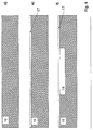
- a first exemplary process is in essential steps in FIGS FIGS. 1 and 2 shown. Variations of this first process will be described later.
- the basic manufacturing process begins with a first wafer 1, which is preferably of the same material as a second wafer 5 used later.
- a layer 2 is deposited, which serves the later connection.
- silicon wafers these are formed as an SiO 2 layer 2 by oxidation.
- a window is opened and the subsequent pressure sensor cavity 4 etched.
- This etching preferably takes place by means of a DRIE or plasma etching step, since in particular the former leads to straight walls 3.
- the upper wafer 5 is also provided with an oxide layer and bonded and ground on the first wafer 1.
- the bonding process is preferably carried out in a vacuum. This leads to a cavity which is not filled with gas and excludes a later temperature dependence of the internal pressure in the cavity. This process creates in the area of the cavity 4 a membrane whose thickness is determined by the grinding process.
- the result is a wafer package that can be used in a standard CMOS process or standard bipolar process like normal SOI material.
- micromechanical structures 6 can then be etched into the surface 11. ( Fig. 1e ).
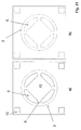
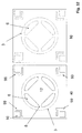
- these micromechanical structures 6 are, for example, trench structures which form approximately closed rings or quadrilaterals which are interrupted only by a few webs 8 (FIG. Fig. 2 ). This creates in the middle of a central plate 12 - Boss called - which represents a stiffener due to the greater thickness.
- the bottom of the trenches 6 is a membrane of lesser thickness. This typically absorbs significantly less force. It is important here that the outer edge of the trench 6 is sufficiently far away from the wall of the cavity 3, since otherwise small adjustment errors in the production would have a great effect on the mechanical stress and thus on the measurement result. This is a significant innovation. The manufacturing reproducibility of the sensor properties would thus suffer, which would result in an increased calibration effort and thus corresponding costs.
- the pressure on the central plate 12 is derived almost exclusively via mechanical tension on the webs 8. Therefore, it makes sense to place on these webs the components 9, which are sensitive to mechanical stress and should detect this stress. These are then connected via lines to the terminals 10. The trenches thus adjust the mechanical stress field compared to the stress-sensitive electronic components.
- the cavity can also be etched into the upper wafer. This is in the FIGS. 3 and 4 represented correspondingly in steps a to f,
- a major disadvantage of the two preceding processes is the lack of a natural etch stop for the etching of the trenches 6. Therefore, the thickness of the Membrane at the bottom of the trenches 7 difficult to control. The relative error is therefore relatively high, which leads to a scattering of the sensor parameters.
- a third exemplary process that does not suffer from this disadvantage is in essential steps in FIGS FIGS. 5 to 10 and steps a to j are shown.
- the manufacturing process begins with a first wafer 13, which is preferably of the same material as the second wafer 16 used later.
- a connecting layer in the case of silicon wafers, an SiO 2 layer 14 on this SiO 2 layer, a further layer, such as a poly-silicon layer or amorphous silicon layer 15 is deposited and oxidized superficially ( Fig. 5c ).
- the deposition of this layer can typically be very well controlled, and is therefore much more precise in its result than the etching of the trenches in the first two processes described.
- the second wafer 16 is also oxidized, so that an oxide layer 17 is also formed. In this at least one window is opened and the later cavity 18 is etched. This etching is preferably carried out by a DRIE etching step, since this leads to straight walls ( Fig. 6f ).
- the etching of the cavity 18 in the upper wafer 13 will not be further described below, but of course also possible.
- the upper first wafer 13 is bonded to the second wafer 16 ( Fig. 7 ) and then sanded ( Fig. 8 ).
- the bonding process is preferably carried out again in a vacuum in order to preclude a later temperature dependence of the internal pressure in the cavity 18. This creates a diaphragm in the region of the cavity whose thickness is determined by the grinding process.
- the result is again a wafer package, which in principle can be used like a standard wafer in a standard CMOS process or standard bipolar process.
- micromechanical structures for example trenches 19, can then be etched into the surface 24, as in the previously described processes ( Fig. 10 ).
- these micromechanical structures 19 are again trench structures, for example, which form approximately closed rings or quadrilaterals which are interrupted only by a few webs 20. This results again in the middle of a central plate 21, which represents a stiffener due to the greater thickness.
- the bottom of the trenches 19 is a membrane of lesser thickness 25. This takes again virtually no forces.
- stress-sensitive sensors can be fabricated on the membrane after their manufacture prior to fabrication of the trenches (6 or 19).
- CMOS complementary metal-oxide-semiconductor
- bipolar process a CMOS process, a p-doped substrate is preferably used.
- piezo-resistive resistors can be placed on the webs 20, 8 and interconnected as a Wheatstone bridge.
- these have the disadvantage that they must first be brought to operating temperature and consume a relatively large amount of electrical energy in a measurement. They are therefore unsuitable for energy-autarkic systems.
- the invention thus also has the object, as already described above, of eliminating this problem.
- transistors 85,86,87,88 a Wheatstone bridge, which can be tapped at the two terminals 89,90.
- the transistors 87 and 85 are constructed similarly oriented and the transistor pair 88,86 also the same orientation, but perpendicular to the transistor pair 87,85.
- this circuit is very sensitive to manufacturing errors.
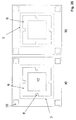
- Fig. 11 shows the exemplary layout of such a self-aligned transistor.
- the p + contact implantations 80 and 79 are shaded by the poly gate 81 in such a way that the same transistor channel length and transistor width always remain even when offset.
- the poly gate 81 shadows the n + channel stop implant from.
- the gate is connected via a low-resistance poly line.
- a reference voltage source In order to bring the transistors in the respective correct operating point, it is expedient to integrate a reference voltage source with the pressure sensor.
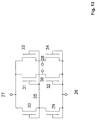
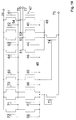
- the transistors 31,32,33,34 again form a Wheatstone bridge, which can be tapped at the terminals 28,36. Both are connected as MOS diodes by connecting the gate to the drain.
- the reference voltage of transistor 30 is connected to the gate of transistor 31 and 33.
- the reference voltage of transistor 29 is connected to the gate of transistors 32 and 34.
- the drain of transistor 29 is at the potential of terminal 26. This terminal is typically grounded in p-channel transistors. Therefore, the drains of transistors 32 and 34 are also connected to this terminal.
- the transistors are preferably made with the same geometric dimensions.
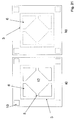
- the layout example of a local Wheatstone MOS bridge is in Fig. 14 given. Are the transistors like in Fig. 14 arranged, the transistors 31 and 34 are the same orientation. The transistors 23 and 33 are likewise mutually oriented, but perpendicular to the transistors 31 and 34.
- Fig. 14 shows an exemplary arrangement.
- a field oxide In order to keep the mechanical stresses on the membrane small, this is not provided with a field oxide but only with a very thin gate oxide of only a few nm and a suitable passivation. If the application of a field oxide is unavoidable, a high degree of symmetry makes sense, in order to keep parasitic effects the same on all stress-sensitive components.
- the passivation can, for example, in a silicon pressure sensor consist of silicon nitride. This has a low hydrogen diffusion coefficient and therefore protects the device against ingress and egress of protons, which can lead to a drift of the p-resistors and p-channel transistors, in particular with permanently applied voltage and high operating temperature. This effect is known as NBTI.
- the diaphragm of the exemplary pressure sensor is only covered with the gate oxide and the passivation layer silicon nitride.
- the leads on the die are preferably not in metal, which has a high coefficient of thermal expansion, in particular with respect to silicon, but in the wafer material, in the case of silicon as highly doped layer or highly doped poly-silicon or, if not possible, as highly doped amorphous or polycrystalline silicon executed.
- the drain and source leads of transistors 26, 28, 35, 36 are in this example ( Fig. 14 ) are performed, for example, as p + implantations 36, 35, 26, 28.
- the gates and their leads are exemplified in Pol silicon 33,39,31 and 32,34,38.
- area 40 which is n-doped, no channel is formed due to the field threshold in the example. This is possible only at the edge of the poly gates. Therefore, an n + channel stopper 37 is implanted which cuts off parasitic channels.
- This exemplary all-silicon design thus makes it possible to build the element sensitive to mechanical stress very small and insensitive to manufacturing tolerances and thermo-mechanical stress by foreign materials, which further reduces the sensitivity to inhomogeneous stress distributions. Despite these efforts, there are still marginal differences between the materials. Therefore, when designing the electronic components on the die, and especially those located on the membrane, attention is paid to maintaining the greatest possible symmetry. Therefore, it makes sense to place components that are used for differentiation - for example, those in Wheatstone bridges or differential amplifiers - as close to each other as possible in order to minimize the influence of manufacturing inhomogeneities.
- Fig. 15 shows another expression of the Wheatstone bridge.
- the reference voltage with which the bridge is operated consisting of the transistors 31,32,33,34, from one of these same bridge, consisting of the transistors 30,29,55,56 generated.
- the reference bridge is short-circuited and thus generates the reference voltage 35, with which the transistors 31,32,33,34 of the first bridge are driven.
- the second bridge is placed on the substrate as far away from the mechanical stresses as possible but still as close to the first bridge as possible. The latter serves to keep the manufacturing fluctuations between the two bridges low.
- the first bridge is placed in the point of appropriate mechanical stress. This is the point at which the highest possible mechanical stress results from deflection of the exemplary membrane, but this stress is still so homogeneous that manufacturing fluctuations can not be noticeable too strongly.
- Fig. 16 shows the placement of the bridges and reference bridges according to Figure 15 .
- Fig. 17 shows the placement of the bridges and reference bridges according to Figure 15 .
- the first level that of the four transistors, the direction of mechanical stress is detected. This is done by comparing the values of perpendicular to each other transistors.
- these four transistors in their entirety 43 are compared with four other identically arranged transistors 58 which are ideally located on the neutral fiber, close to the first four 43 but in a mechanically less stressed region.
- the mechanically induced offset of the bridge is distinguished from the adjustment error during production. If the sensor is symmetrical, then it makes sense to install another eight transistors according to the symmetry axis. in the Example ( Fig. 17 ), these are four pairs of sensors 44, 57, 41, 60, 42, 59, 43, 58, each pair consisting of two by four transistors.
- FIG. 34 shows the associated interconnection with a reference voltage source consist of the transistors 108,109.
- the four transistors 104, 105, 106, 107 connected to a Wheatstone bridge have a common gate 110, which simplifies the layout.
- the bridge is supplied with voltage via terminals 103 and 102. In the case of mechanical stress on the bridge, an electrical voltage occurs at terminals 111, 112.
- Fig. 35 shows another expression of this bridge. If the channel stopper 37 is omitted in the middle of the bridge, the result is a field plate-like transistor 115 with four terminals. ( Fig. 37 )
- the equivalent circuit of the transistor 115 shows Fig. 36 , Then there are the transistors 114 and 113 added, on the one hand raise the power consumption 114 and on the other hand reduce the signal level 113. But the design and thus the space requirement can be minimized, which is very useful in some applications.
- FIG Fig. 18 An alternative layout arrangement of the transistors of a sensor element 41, 42, 43, 44, 57, 58, 59, 60 is shown in FIG Fig. 18 shown.
- the four transistors 44,45,46,47 are arranged in a star shape. They have a common drain contact 50, which is connected via a feed line 49 to a power source which is not located on the diaphragm of the pressure sensor.
- the gates of transistors 44, 45, 46, 47 are connected to a poly line 48.
- the source contacts are each connected to a heavily doped p + line 51,52,53,54.
- the four transistors are, for example, parts of a differential amplifier, like him Fig. 19 shows. All other transistors of the Fig. 19 are not on the membrane but the substrate without underlying Cavity. It will be appreciated that half of the four transistors, such as transistors 45 and 44, would already be sufficient to form a differential amplifier. For symmetry reasons, however, the variant with four transistors makes sense.
- the circuit consists of two differential amplifiers.
- the left (transistors 65 to 73) is shorted in the output and input and operates as a reference voltage source for the operation of the second. These transistors are free of mechanical stress in an area.
- the previously discussed transistors 44,45,46,47 form the differential stage with the respectively associated "working resistances" 61,62,63,64.
- the current source 74 energizes the differential amplifier formed in this way.
- the transistor 74 is an n-channel transistor in this example.
- the outputs of the differential amplifier 77,78 reflect in operation an unbalance of the transistors 44,45,46,47 due to mechanical stress. Since transistors 46 and 44 are oriented differently than transistors 45 and 47, uniaxial mechanical stress results in an output signal 77, 78.
- the differential amplifier is brought in this example by an identically constructed short-circuited reference differential amplifier in the operating point.
- This and the transistors 61,62,63,64,74 are expediently not on the membrane but in a region of the die which is almost free from mechanical stress. In order to ensure the conformity of the electrical parameters of the components in a stress-free state, they should nevertheless be placed as close as possible to the other transistors. Appropriately, therefore, the alignment and the layout of all elements as close to each other in the same orientation and the same layout is performed so that in particular the current mirror pairs are well matched.
- FIGS. 20 to 25 show different designs of trenches and cavities.
- the senor is suspended on webs 94. These are ideally no extension of the webs 8, where the boss 12 is attached. As a result, mechanical stress is transmitted only indirectly from the outside to the sensors 9.
- FIGS. 29 and 30 show corresponding exemplary formations.
- the advantage of such a design lies in the small opening and thus in the very slight loss of stability compared to a sensor in which the cavity was etched from the back.
- the bonding system is usually made of metal with a significantly different thermal expansion coefficient. Furthermore, the metal leads to hysteresis effects. Therefore, it makes sense to decouple the bond pads 10 as far as possible from the rest of the sensors. This can be done by mechanical guard rings in the form of trenches 157, which are for example placed as far as possible around the pads or parts to be protected ( Fig. 32 ).
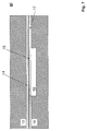
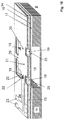
- the peculiarities of the construction of a low-stress transistor will be described, which is sensitive to mechanical stresses and which can be used in a reversibly deformable bending element 8a of semiconductor material of a microelectromechanical semiconductor component.
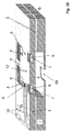
- the construction in which the transistor for stress sensitive transistor according to Fig. 39 is introduced it can be as, for example, previously based on the FIGS. 1 to 10, 20 to 32, 34, 35, 37 and 38 explained, achieved.
- the transistor is within a ridge 8 of the cavity 4 covering the area of the device wafer 5.
- a ventilation channel lead to the cavity 4, but this is irrelevant to the design and operation of the transistor.
- the transistor is formed in an active area well 78a which is implanted in the p-doped semiconductor substrate of the device wafer 5. Within the well 78a, heavily p + doped source and drain regions 79, 80 are formed, again by implantation. Between the mutually facing ends of these two areas 79 and 80 is the actual channel region of the transistor. The entire upper side of the active-area well 78a is covered by thin gate oxide (SI oxide) 81a, wherein the transistor gate 81 made of poly-silicon is arranged in the region of the channel region on this oxide.
- SI oxide thin gate oxide
- the supply lines to the drain and source regions 79, 80 are also formed by highly doped p + regions, which have been produced by implantation, and extend outside the region spanning the cavity 4 (ie, to outside the membrane). of the device wafer 5 where they are connected to metal lines 79a, 80a.
- the lead 84 to the transistor gate 81 is made by a line of poly-silicon, as also in Fig. 40 can be seen.
- each transistor should be arranged in a separate active area.
- the transistor is thus determined both in the length L and in the width B solely and solely by the geometry of the poly-silicon gate 81.
- the implanted source and drain contact regions 79, 80 extend into the edge recesses 201, 202 of the gate 81 Fig. 41 the terminal regions 79, 80 are defined by openings in the implantation mask.
- the gate 81 serves as an ion implantation masking material.
- Fig. 42 shows the layout of an alternative semiconductor device according to the invention with channel implantation 205 (dashed).
- channel implantation 205 (dashed).
- this is a p-implantation that was performed prior to the fabrication of the p-channel transistor
- Gates 81 is introduced.
- This channel implantation is thus initially not adjusted in the x and y direction with respect to the polysilicon gate 81.
- this channel implantation overlaps in the region of the transverse edge recesses 201, 202 of the gate 81 the (later) lead contact areas 79, 80, which are later introduced into the active area 200 with the aid of the transverse edge recesses 201, 202 as ion implantation masking.
- the particular shape and patterning of the poly-silicon gate 81 as an ion implantation masking material to define the width-to-length ratio of the channel region by self-alignment is exemplified by FIG Fig. 42 to recognize.
- the gate 81 has transverse edge recesses 201, 202 as well as longitudinal edge recesses 207, 208, each of which is U-shaped in plan view.
- the base edges 207a and 208a of the longitudinal edge recesses 207,208 lie with the opposite side edges 201b and 202b on a common line.
- the width B of the channel region is therefore defined by the width of the transverse edge recesses 201, 202 directly to the terminal regions 79, 80 contacting the channel region.
- the channel region is well-defined in terms of its width B, through the channel stopper implantations 206, in which the base edges 207a, 208a serve as the masking edge.
- the width extension of the longitudinal edge recesses 207, 208 are defined by their longitudinal edges 207b, 208b. The smaller the distance of these side edges 207b, 208b from the base edges 201a, 202a, the more accurately the width of the channel region in the end regions of the channel region (as viewed along its longitudinal extent) can be determined.
Landscapes
- Engineering & Computer Science (AREA)
- Microelectronics & Electronic Packaging (AREA)
- Computer Hardware Design (AREA)
- Physics & Mathematics (AREA)
- Manufacturing & Machinery (AREA)
- Chemical & Material Sciences (AREA)
- Analytical Chemistry (AREA)
- Geometry (AREA)
- Mechanical Engineering (AREA)
- General Physics & Mathematics (AREA)
- Thermal Sciences (AREA)
- Pressure Sensors (AREA)
- Measuring Fluid Pressure (AREA)
- Micromachines (AREA)
Claims (5)
- Transistor, notamment pour une utilisation comme composant sensible à des tensions mécaniques dans un composant semi-conducteur micro-électromécanique tel un capteur de pression ou d'accélération, avec- des zones de drain et de source (79, 80) et une grille (81),- un substrat semi-conducteur (1, 5) dans la face supérieure duquel une zone active (78a, 200) en un matériau d'un premier type de conductivité est introduite par implantation ionique,- une zone de canal semi-conductrice de longueur (L) et largeur (B) définies étant formée à l'intérieur de la zone active (78a, 200),- une zone de contact (79, 80) respective en un matériau d'un second type de conductivité jouxtant les extrémités, en étendue longitudinale, de la zone de canal dans la zone active (78a, 200), et- la zone de canal étant recouverte d'un matériau de masquage pour implantation ionique comme grille (81) et comportant des bords transversaux définissant la longueur (L) de la zone de canal ainsi que des bords longitudinaux définissant la largeur (B) de la zone de canal,caractérisé en ce que- le matériau de masquage pour implantation ionique comprend à ses bords transversaux opposés et alignés sur les extrémités, en étendue longitudinale, de la zone de canal, un évidement de bord (201, 202) respectif jusque dans lesquels s'étendent les zones de contact (79, 80) jouxtant la zone de canal, et en ce que- des zones d'implantation ionique (82, 83, 206) délimitant la zone de canal latéralement sont introduites le long des bords longitudinaux du matériau de masquage pour implantation ionique, dont les limites vers la zone de canal sont alignées sur les bords longitudinaux du matériau de masquage pour implantation ionique.
- Transistor selon la revendication 1, caractérisé en ce que les évidements de bord (201, 202) aux bords transversaux du matériau de masquage pour implantation ionique sont formés, en vue de dessus sur le matériau de masquage pour implantation ionique, sensiblement en U et comportent deux bords latéraux (201b, 202b) opposés et parallèles l'un à l'autre et comprenant un bord de base (201a, 201b) reliant ceux-ci, les bords latéraux (201b, 202b) des deux évidements de bord (201, 202) étant situés par paires sur une ligne commune.
- Transistor selon la revendication 2, caractérisé en ce que les bords latéraux du matériau de masquage pour implantation ionique comprennent chacun, en vue de dessus sur le matériau de masquage pour implantation ionique, des évidements de bord en U (207, 208) avec un bord de base respectif (207a, 208a) s'étendant dans la direction de l'étendue longitudinale du canal et avec des bords latéraux (207b, 208b) partant de celui-ci de préférence sensiblement à angle droit et en ce que les bords de base (207a, 208a) des évidements de bords longitudinaux (207, 208) du matériau de masquage pour implantation ionique sont situés chacun sur la ligne commune des bords latéraux (201b, 202b) des évidements de bords transversaux (201, 202) du matériau de masquage pour implantation ionique.
- Transistor selon l'une des revendications 1 à 3, caractérisé en ce que, en-dessous du matériau de masquage pour implantation ionique, une implantation de canal (205) est introduite dans la zone active (78a, 200).
- Transistor selon l'une des revendications 1 à 4, caractérisé en ce que le premier type de conductivité est le type de conductivité n et le seconde type de conductivité est le type de conductivité p.
Priority Applications (1)
| Application Number | Priority Date | Filing Date | Title |
|---|---|---|---|
| EP11700251.9A EP2524389B1 (fr) | 2010-01-11 | 2011-01-10 | Capteur semi-conducteur |
Applications Claiming Priority (3)
| Application Number | Priority Date | Filing Date | Title |
|---|---|---|---|
| EP10150405 | 2010-01-11 | ||
| EP11700251.9A EP2524389B1 (fr) | 2010-01-11 | 2011-01-10 | Capteur semi-conducteur |
| PCT/EP2011/050210 WO2011083159A2 (fr) | 2010-01-11 | 2011-01-10 | Composant semi-conducteur |
Publications (2)
| Publication Number | Publication Date |
|---|---|
| EP2524389A2 EP2524389A2 (fr) | 2012-11-21 |
| EP2524389B1 true EP2524389B1 (fr) | 2016-06-15 |
Family
ID=44305870
Family Applications (5)
| Application Number | Title | Priority Date | Filing Date |
|---|---|---|---|
| EP20110700163 Active EP2523896B1 (fr) | 2010-01-11 | 2011-01-10 | Composant semi-conducteur microélectromécanique et son procédé de fabrication |
| EP11700251.9A Active EP2524389B1 (fr) | 2010-01-11 | 2011-01-10 | Capteur semi-conducteur |
| EP20110700061 Active EP2524198B1 (fr) | 2010-01-11 | 2011-01-10 | Composant semi-conducteur microélectromécanique et son procédé de fabrication |
| EP20110700636 Active EP2524390B1 (fr) | 2010-01-11 | 2011-01-10 | Élément capteur semi-conducteur microélectromécanique |
| EP20110700162 Active EP2523895B1 (fr) | 2010-01-11 | 2011-01-10 | Composant semi-conducteur microélectromécanique |
Family Applications Before (1)
| Application Number | Title | Priority Date | Filing Date |
|---|---|---|---|
| EP20110700163 Active EP2523896B1 (fr) | 2010-01-11 | 2011-01-10 | Composant semi-conducteur microélectromécanique et son procédé de fabrication |
Family Applications After (3)
| Application Number | Title | Priority Date | Filing Date |
|---|---|---|---|
| EP20110700061 Active EP2524198B1 (fr) | 2010-01-11 | 2011-01-10 | Composant semi-conducteur microélectromécanique et son procédé de fabrication |
| EP20110700636 Active EP2524390B1 (fr) | 2010-01-11 | 2011-01-10 | Élément capteur semi-conducteur microélectromécanique |
| EP20110700162 Active EP2523895B1 (fr) | 2010-01-11 | 2011-01-10 | Composant semi-conducteur microélectromécanique |
Country Status (4)
| Country | Link |
|---|---|
| US (7) | US9126826B2 (fr) |
| EP (5) | EP2523896B1 (fr) |
| CN (3) | CN102741674A (fr) |
| WO (5) | WO2011083162A2 (fr) |
Cited By (1)
| Publication number | Priority date | Publication date | Assignee | Title |
|---|---|---|---|---|
| DE102020123930B3 (de) | 2020-09-15 | 2021-11-04 | Elmos Semiconductor Se | Verfahren zur ISO 26262 konformen Auswertung eines Drucksensorsignals |
Families Citing this family (56)
| Publication number | Priority date | Publication date | Assignee | Title |
|---|---|---|---|---|
| EP2523896B1 (fr) | 2010-01-11 | 2014-06-11 | ELMOS Semiconductor AG | Composant semi-conducteur microélectromécanique et son procédé de fabrication |
| DE102011081002B4 (de) | 2011-08-16 | 2020-01-16 | Robert Bosch Gmbh | Herstellungsverfahren für ein mikromechanisches Bauteil |
| DE102011112935B4 (de) * | 2011-09-13 | 2015-02-12 | Micronas Gmbh | Kraftsensor |
| FR2982023B1 (fr) * | 2011-10-26 | 2015-03-06 | Auxitrol Sa | Structure micromecanique a membrane deformable et a protection contre de fortes deformations |
| US9021887B2 (en) | 2011-12-19 | 2015-05-05 | Infineon Technologies Ag | Micromechanical semiconductor sensing device |
| US9184138B2 (en) * | 2011-12-29 | 2015-11-10 | Stmicroelectronics (Grenoble 2) Sas | Semiconductor integrated device with mechanically decoupled active area and related manufacturing process |
| US8590389B2 (en) * | 2012-02-10 | 2013-11-26 | Metrodyne Microsystems Corporation, R.O.C. | MEMS pressure sensor device and manufacturing method thereof |
| US20130334531A1 (en) * | 2012-06-15 | 2013-12-19 | Franz Jost | Systems and methods for measuring temperature and current in integrated circuit devices |
| WO2014098567A1 (fr) * | 2012-12-21 | 2014-06-26 | Mimos Berhad | Capteur de pression |
| FR3000841A1 (fr) * | 2013-01-09 | 2014-07-11 | St Microelectronics Rousset | Procede de realisation d'un dispositif metallique loge dans un logement ferme au sein d'un circuit integre, et circuit integre correspondant |
| US9176018B2 (en) * | 2013-02-22 | 2015-11-03 | Bin Qi | Micromachined ultra-miniature piezoresistive pressure sensor and method of fabrication of the same |
| US9156676B2 (en) * | 2013-04-09 | 2015-10-13 | Honeywell International Inc. | Sensor with isolated diaphragm |
| DE102014010116B4 (de) | 2013-04-29 | 2018-11-15 | Elmos Semiconductor Aktiengesellschaft | MEMS Sensor für schwierige Umgebungen und Medien |
| TWI514938B (zh) * | 2013-12-26 | 2015-12-21 | Ind Tech Res Inst | 撓性電子模組 |
| WO2015114635A1 (fr) | 2014-02-01 | 2015-08-06 | Ezmems Ltd. | Dispositif de puce permettant de surveiller et de réguler un écoulement de fluide, et ses procédés de fabrication |
| US9941472B2 (en) | 2014-03-10 | 2018-04-10 | International Business Machines Corporation | Piezoelectronic device with novel force amplification |
| US9251884B2 (en) | 2014-03-24 | 2016-02-02 | International Business Machines Corporation | Non-volatile, piezoelectronic memory based on piezoresistive strain produced by piezoelectric remanence |
| US9663354B2 (en) | 2014-05-14 | 2017-05-30 | Infineon Technologies Ag | Mechanical stress-decoupling in semiconductor device |
| CN104034454B (zh) | 2014-06-13 | 2016-05-25 | 江苏多维科技有限公司 | 一种用于多物理量测量的传感器芯片及其制备方法 |
| US9513242B2 (en) | 2014-09-12 | 2016-12-06 | Honeywell International Inc. | Humidity sensor |
| CN105527042B (zh) * | 2014-10-15 | 2020-06-05 | 浙江盾安人工环境股份有限公司 | 压力传感器及其制造方法 |
| US9263664B1 (en) * | 2014-10-31 | 2016-02-16 | International Business Machines Corporation | Integrating a piezoresistive element in a piezoelectronic transistor |
| GB2532806A (en) | 2014-11-25 | 2016-06-01 | Continental Automotive Systems Us Inc | Piezoresistive pressure sensor device |
| WO2016130123A1 (fr) * | 2015-02-12 | 2016-08-18 | Honeywell International Inc. | Dispositifs micromécaniques dotés d'une meilleure structure d'évidement ou de cavité |
| JP6341190B2 (ja) * | 2015-02-16 | 2018-06-13 | 株式会社デンソー | 半導体装置の製造方法 |
| EP3259581B1 (fr) | 2015-02-17 | 2020-01-29 | Honeywell International Inc. | Capteur d'humidité et procédé de fabrication du capteur |
| US9719872B2 (en) | 2015-09-29 | 2017-08-01 | Rosemount Inc. | High over-pressure capable silicon die pressure sensor with extended pressure signal output |
| US10060813B2 (en) | 2015-09-29 | 2018-08-28 | Rosemount Inc. | High over-pressure capable silicon die pressure sensor |
| JP6300773B2 (ja) * | 2015-10-23 | 2018-03-28 | 三菱電機株式会社 | 半導体圧力センサ |
| US9804046B2 (en) * | 2015-10-27 | 2017-10-31 | DunAn Sensing, LLC | Pressure sensor with support structure for non-silicon diaphragm |
| US9899527B2 (en) * | 2015-12-31 | 2018-02-20 | Globalfoundries Singapore Pte. Ltd. | Integrated circuits with gaps |
| EP3211393A1 (fr) | 2016-02-29 | 2017-08-30 | ETH Zürich | Dispositif mems à l'aide d'une couche de dispositif en tant que membrane libérée |
| US9964458B2 (en) | 2016-05-12 | 2018-05-08 | Continental Automotive Systems, Inc. | Pressure sensor device with anchors for die shrinkage and high sensitivity |
| EP3244201B1 (fr) | 2016-05-13 | 2021-10-27 | Honeywell International Inc. | Capteur d'humidité à base de tec avec couche barrière protégeant le diélectrique de grille |
| DE102016210384A1 (de) * | 2016-06-13 | 2017-12-14 | Robert Bosch Gmbh | Mikromechanisches Bauteil und Verfahren zum Herstellen eines mikromechanischen Bauteils |
| DE102016111836B4 (de) | 2016-06-28 | 2024-02-15 | Infineon Technologies Ag | Halbleiterbauelemente und Verfahren zum Bilden eines Halbleiterbauelements |
| JP6555214B2 (ja) * | 2016-08-25 | 2019-08-07 | 株式会社デンソー | 圧力センサ |
| US10203258B2 (en) * | 2016-09-26 | 2019-02-12 | Rosemount Inc. | Pressure sensor diaphragm with overpressure protection |
| JP6759454B2 (ja) * | 2016-09-27 | 2020-09-23 | ローズマウント インコーポレイテッド | 高圧超高圧シリコンダイ圧力センサ |
| CN106556386B (zh) * | 2016-11-15 | 2019-11-08 | 东南大学 | 硅基微壳体谐振器及其制备方法 |
| DE102017102545B4 (de) * | 2017-02-09 | 2018-12-20 | Infineon Technologies Ag | Halbleitervorrichtung, Drucksensor, Mikrofon, Beschleunigungssensor und Verfahren zum Bilden einer Halbleitervorrichtung |
| IT201700045285A1 (it) * | 2017-04-26 | 2018-10-26 | St Microelectronics Srl | Trasduttore microelettromeccanico basato su trincea e metodo di fabbricazione del trasduttore microelettromeccanico |
| DE102017210691A1 (de) * | 2017-06-26 | 2018-12-27 | Robert Bosch Gmbh | Verfahren zur Herstellung von mikromechanischen Sensoren |
| US10809621B2 (en) * | 2017-12-21 | 2020-10-20 | Commissariat à l'énergie atomique et aux énergies alternatives | Process for the exposure of a region on one face of an electronic device |
| IT201800001092A1 (it) | 2018-01-16 | 2019-07-16 | St Microelectronics Srl | Sensore di pressione piezoresistivo microelettromeccanico con capacita' di auto-diagnosi e relativo procedimento di fabbricazione |
| JP6922788B2 (ja) * | 2018-03-05 | 2021-08-18 | 三菱電機株式会社 | 半導体圧力センサ |
| RU197682U1 (ru) * | 2019-12-27 | 2020-05-21 | Федеральное государственное автономное образовательное учреждение высшего образования "Национальный исследовательский Томский государственный университет" (ТГУ, НИ ТГУ) | Полупроводниковый датчик давления |
| US11473991B2 (en) | 2019-12-29 | 2022-10-18 | Measurement Specialties, Inc. | Low-pressure sensor with stiffening ribs |
| DE102021200720B4 (de) | 2021-01-27 | 2023-08-03 | Infineon Technologies Ag | Transistorbasierter stress-sensor und verfahren zum ermitteln einer gradienten-kompensierten mechanischen spannungskomponente |
| US11692895B2 (en) * | 2021-03-30 | 2023-07-04 | Rosemount Aerospace Inc. | Differential pressure sensor |
| CN113432777B (zh) * | 2021-05-28 | 2023-02-28 | 歌尔微电子股份有限公司 | Mems压力传感器制造方法及mems压力传感器 |
| CN114199353B (zh) * | 2021-12-09 | 2024-03-05 | 上海辰竹仪表有限公司 | 应变桥输入采样电路和称重系统 |
| CN114758730B (zh) * | 2022-01-05 | 2024-08-16 | 西安理工大学 | 等离子体活性粒子与绝缘材料表面作用的仿真方法 |
| US12281996B2 (en) | 2022-06-22 | 2025-04-22 | Globalfoundries U.S. Inc. | Semiconductor structure including photodiode-based fluid sensor and methods |
| DE102023103998A1 (de) * | 2023-02-17 | 2024-08-22 | Albert-Ludwigs-Universität Freiburg | Schaltungsanordnung zur Ansteuerung wenigstens eines Stresssensors und Stresskartierungssystem |
| DE102024105120A1 (de) * | 2024-02-23 | 2025-08-28 | Lpkf Laser & Electronics Se | Verfahren zur Integration und/oder Bearbeitung wenigstens eines Substrats sowie Substratstapel |
Family Cites Families (53)
| Publication number | Priority date | Publication date | Assignee | Title |
|---|---|---|---|---|
| US4467656A (en) | 1983-03-07 | 1984-08-28 | Kulite Semiconductor Products, Inc. | Transducer apparatus employing convoluted semiconductor diaphragms |
| US4658279A (en) * | 1983-09-08 | 1987-04-14 | Wisconsin Alumini Research Foundation | Velocity saturated strain sensitive semiconductor devices |
| US5069419A (en) * | 1989-06-23 | 1991-12-03 | Ic Sensors Inc. | Semiconductor microactuator |
| JPH03141645A (ja) * | 1989-07-10 | 1991-06-17 | Texas Instr Inc <Ti> | ポリサイドによる局所的相互接続方法とその方法により製造された半導体素子 |
| FR2695787B1 (fr) * | 1992-09-11 | 1994-11-10 | Suisse Electro Microtech Centr | Transducteur capacitif intégré. |
| EP0822579B1 (fr) * | 1996-07-31 | 2004-07-21 | STMicroelectronics S.r.l. | Des structures intégrés d'un matériau semi-conducteur et un procédé pour leur fabrication |
| DE19632060B4 (de) * | 1996-08-09 | 2012-05-03 | Robert Bosch Gmbh | Verfahren zur Herstellung eines Drehratensensors |
| EP0863392B1 (fr) * | 1997-03-04 | 2000-08-09 | STMicroelectronics S.r.l. | Méthode pour fabriquer des indicateurs de pression micromécaniques |
| US6006607A (en) | 1998-08-31 | 1999-12-28 | Maxim Integrated Products, Inc. | Piezoresistive pressure sensor with sculpted diaphragm |
| US6351996B1 (en) | 1998-11-12 | 2002-03-05 | Maxim Integrated Products, Inc. | Hermetic packaging for semiconductor pressure sensors |
| DE10032579B4 (de) * | 2000-07-05 | 2020-07-02 | Robert Bosch Gmbh | Verfahren zur Herstellung eines Halbleiterbauelements sowie ein nach dem Verfahren hergestelltes Halbleiterbauelement |
| EP1307720A1 (fr) * | 2000-07-06 | 2003-05-07 | California Institute Of Technology | Capteur de pression a surface micro-usinee et application a haute pression |
| US20020127760A1 (en) * | 2000-08-02 | 2002-09-12 | Jer-Liang Yeh | Method and apparatus for micro electro-mechanical systems and their manufacture |
| ITVA20000042A1 (it) * | 2000-12-15 | 2002-06-15 | St Microelectronics Srl | Sensore di pressione monoliticamente integrato e relativo processo direalizzazione. |
| JP2002190607A (ja) * | 2000-12-22 | 2002-07-05 | Denso Corp | 半導体装置及びその製造方法 |
| FR2822817B1 (fr) | 2001-03-28 | 2003-05-30 | Commissariat Energie Atomique | Procede de fabrication d'une structure a membrane micro-usinee |
| US6465355B1 (en) * | 2001-04-27 | 2002-10-15 | Hewlett-Packard Company | Method of fabricating suspended microstructures |
| DE10152254A1 (de) * | 2001-10-20 | 2003-04-30 | Bosch Gmbh Robert | Mikromechanisches Bauelement und entsprechendes Herstellungsverfahren |
| DE10160830A1 (de) * | 2001-12-11 | 2003-06-26 | Infineon Technologies Ag | Mikromechanische Sensoren und Verfahren zur Herstellung derselben |
| US7253488B2 (en) * | 2002-04-23 | 2007-08-07 | Sharp Laboratories Of America, Inc. | Piezo-TFT cantilever MEMS |
| US7276798B2 (en) * | 2002-05-23 | 2007-10-02 | Honeywell International Inc. | Integral topside vacuum package |
| US6936491B2 (en) | 2003-06-04 | 2005-08-30 | Robert Bosch Gmbh | Method of fabricating microelectromechanical systems and devices having trench isolated contacts |
| US7111518B1 (en) * | 2003-09-19 | 2006-09-26 | Silicon Microstructures, Inc. | Extremely low cost pressure sensor realized using deep reactive ion etching |
| WO2005086535A1 (fr) * | 2004-03-09 | 2005-09-15 | Matsushita Electric Industrial Co., Ltd. | Microphone a condensateur a electret |
| KR100622955B1 (ko) * | 2004-04-06 | 2006-09-18 | 삼성전자주식회사 | 박막 벌크 음향 공진기 및 그 제조방법 |
| DE102005004877A1 (de) * | 2005-02-03 | 2006-08-10 | Robert Bosch Gmbh | Mikromechanisches Bauelement und entsprechendes Herstellungsverfahren |
| WO2007004119A2 (fr) * | 2005-06-30 | 2007-01-11 | Koninklijke Philips Electronics N.V. | Procede de fabrication d'un element microelectromecanique |
| WO2007037926A2 (fr) * | 2005-09-23 | 2007-04-05 | Sharp Laboratories Of America, Inc. | Capteur de pixels mems |
| CN101273255B (zh) * | 2005-11-15 | 2010-05-19 | 三菱电机株式会社 | 半导体压力传感器及其制造方法 |
| JP2007142041A (ja) * | 2005-11-16 | 2007-06-07 | Toshiba Corp | 半導体装置 |
| WO2007069365A1 (fr) * | 2005-12-14 | 2007-06-21 | Matsushita Electric Industrial Co., Ltd. | Structure de diaphragme de mems et son procede de fabrication |
| WO2007091657A1 (fr) | 2006-02-10 | 2007-08-16 | Tokyo Electron Limited | structure membranaire et son procEDE de fabrication |
| TW200738028A (en) * | 2006-02-24 | 2007-10-01 | Yamaha Corp | Condenser microphone |
| GB0605576D0 (en) * | 2006-03-20 | 2006-04-26 | Oligon Ltd | MEMS device |
| JP4966370B2 (ja) * | 2006-03-30 | 2012-07-04 | パルス・エムイーエムエス・アンパルトセルスカブ | シングルダイ型mems音響トランスデューサおよび製造方法 |
| DE102006022378A1 (de) * | 2006-05-12 | 2007-11-22 | Robert Bosch Gmbh | Verfahren zur Herstellung eines mikromechanischen Bauelements und mikromechanisches Bauelement |
| EP2038207A2 (fr) * | 2006-06-29 | 2009-03-25 | Nxp B.V. | Dispositif de microsystème électromécanique monocristallin intégré |
| US7880202B2 (en) * | 2006-11-27 | 2011-02-01 | Infineon Technologies Ag | Modulated-Vt transistor |
| US20080190207A1 (en) * | 2007-02-08 | 2008-08-14 | Yang James Y | Ring oscillating digital pressure sensor manufactured by micro-electromechanical system (MEMS) processes |
| DE102007019639A1 (de) * | 2007-04-26 | 2008-10-30 | Robert Bosch Gmbh | Mikromechanisches Bauelement und entsprechendes Herstellungsverfahren |
| EP2008966A3 (fr) * | 2007-06-27 | 2013-06-12 | Sumitomo Precision Products Co., Ltd. | Dispositif MEMS formé à l'intérieur d'une chambre hermétique dotée d'une couche getter |
| JP4607153B2 (ja) * | 2007-07-12 | 2011-01-05 | 株式会社日立製作所 | 微小電気機械システム素子の製造方法 |
| US7795063B2 (en) * | 2007-12-31 | 2010-09-14 | Solid State System Co., Ltd. | Micro-electro-mechanical systems (MEMS) device and process for fabricating the same |
| US8258591B2 (en) * | 2008-01-16 | 2012-09-04 | Solid State System Co., Ltd. | Micro-electro-mechanical systems (MEMS) device |
| US8193596B2 (en) | 2008-09-03 | 2012-06-05 | Solid State System Co., Ltd. | Micro-electro-mechanical systems (MEMS) package |
| US7951636B2 (en) * | 2008-09-22 | 2011-05-31 | Solid State System Co. Ltd. | Method for fabricating micro-electro-mechanical system (MEMS) device |
| TWI444052B (zh) * | 2009-12-17 | 2014-07-01 | Ind Tech Res Inst | 電容式傳感器及其製造方法 |
| US8381596B2 (en) * | 2009-12-21 | 2013-02-26 | Silicon Microstructures, Inc. | CMOS compatible pressure sensor for low pressures |
| EP2523896B1 (fr) | 2010-01-11 | 2014-06-11 | ELMOS Semiconductor AG | Composant semi-conducteur microélectromécanique et son procédé de fabrication |
| DE102010002463A1 (de) * | 2010-03-01 | 2011-09-01 | Robert Bosch Gmbh | Mikromechanisches Drucksensorelement und Verfahren zu dessen Herstellung |
| US8216882B2 (en) * | 2010-08-23 | 2012-07-10 | Freescale Semiconductor, Inc. | Method of producing a microelectromechanical (MEMS) sensor device |
| US8316718B2 (en) * | 2010-08-23 | 2012-11-27 | Freescale Semiconductor, Inc. | MEMS pressure sensor device and method of fabricating same |
| US7998777B1 (en) * | 2010-12-15 | 2011-08-16 | General Electric Company | Method for fabricating a sensor |
-
2011
- 2011-01-10 EP EP20110700163 patent/EP2523896B1/fr active Active
- 2011-01-10 CN CN2011800058613A patent/CN102741674A/zh active Pending
- 2011-01-10 US US13/521,175 patent/US9126826B2/en active Active
- 2011-01-10 US US13/521,168 patent/US9013015B2/en active Active
- 2011-01-10 EP EP11700251.9A patent/EP2524389B1/fr active Active
- 2011-01-10 EP EP20110700061 patent/EP2524198B1/fr active Active
- 2011-01-10 US US13/521,158 patent/US8994128B2/en active Active
- 2011-01-10 WO PCT/EP2011/050213 patent/WO2011083162A2/fr not_active Ceased
- 2011-01-10 WO PCT/EP2011/050211 patent/WO2011083160A2/fr not_active Ceased
- 2011-01-10 EP EP20110700636 patent/EP2524390B1/fr active Active
- 2011-01-10 US US13/521,141 patent/US8975671B2/en active Active
- 2011-01-10 EP EP20110700162 patent/EP2523895B1/fr active Active
- 2011-01-10 WO PCT/EP2011/050209 patent/WO2011083158A2/fr not_active Ceased
- 2011-01-10 CN CN201180005860.9A patent/CN102742012B/zh active Active
- 2011-01-10 CN CN201180005859.6A patent/CN102741979B/zh active Active
- 2011-01-10 US US13/521,146 patent/US8841156B2/en active Active
- 2011-01-10 WO PCT/EP2011/050212 patent/WO2011083161A2/fr not_active Ceased
- 2011-01-10 WO PCT/EP2011/050210 patent/WO2011083159A2/fr not_active Ceased
-
2015
- 2015-02-13 US US14/622,075 patent/US9403676B2/en active Active
- 2015-02-25 US US14/631,064 patent/US9403677B2/en active Active
Non-Patent Citations (1)
| Title |
|---|
| None * |
Cited By (4)
| Publication number | Priority date | Publication date | Assignee | Title |
|---|---|---|---|---|
| DE102020123930B3 (de) | 2020-09-15 | 2021-11-04 | Elmos Semiconductor Se | Verfahren zur ISO 26262 konformen Auswertung eines Drucksensorsignals |
| WO2022057970A1 (fr) | 2020-09-15 | 2022-03-24 | Elmos Semiconductor Se | Procédé d'évaluation conforme à iso 26262 d'un signal de capteur de pression |
| EP4376303A2 (fr) | 2020-09-15 | 2024-05-29 | Elmos Semiconductor SE | Procédé d'évaluation conforme à l'iso26262 d'un signal de capteur de pression |
| US12270720B2 (en) | 2020-09-15 | 2025-04-08 | Elmos Semiconductor Se | Method for ISO 26262-compliant evaluation of a pressure-sensor signal |
Also Published As
Similar Documents
| Publication | Publication Date | Title |
|---|---|---|
| EP2524389B1 (fr) | Capteur semi-conducteur | |
| DE19537285B4 (de) | Verfahren zur Herstellung eines Halbleiterelements mit einer flexiblen Anordnung, Halbleiterelement, Feldeffektsensor mit beweglichem Gate, Verfahren zur Verwendung eines Transistors mit beweglichem Gate als Sensor, sowie kapazitiver Sensor | |
| DE69429381T2 (de) | Verfahren zum Mikro-Bearbeiten eines in der Oberfläche eines Siliziumkörpers integrierten Sensors | |
| DE69627645T2 (de) | Integrierter piezoresistiver Druckwandler und Herstellungsverfahren dazu | |
| DE69900771T2 (de) | Monolithischer Siliziumsensor für Augendruckmessung und Herstellungsverfahren | |
| DE4130044A1 (de) | Halbleiter-drucksensor | |
| EP0720748B1 (fr) | Dispositif de detection micromecanique integre et son procede de production | |
| CH682766A5 (de) | Mikromechanischer Neigungssensor. | |
| DE102017211080B3 (de) | Mikromechanischer Sensor und Verfahren zum Herstellen eines mikromechanischen Sensors und eines mikromechanischen Sensorelements | |
| DE102009039106A1 (de) | Halbleiterbauelement, das einen Drucksensor umfasst | |
| DE10029501C1 (de) | Vertikal-Transistor mit beweglichen Gate und Verfahren zu dessen Herstelllung | |
| DE102019201880B4 (de) | Halbleiter-Drucksensor | |
| EP2550234B1 (fr) | Procédé de fabrication d'un dispositif microélectromécanique et dispositif microélectromécanique | |
| DE102007014468A1 (de) | Drucksensor-Chip | |
| DE10254158A1 (de) | Sensorvorrichtung zur Detektion elektrischer Signale einer biologischen Zelle und Detektionsverfahren | |
| DE102011083962B4 (de) | Halbleiterstruktur mit Lamelle, die durch einen Singulierungsgraben definiert ist | |
| DE10062637B4 (de) | Differenzdrucksensor | |
| DE19543893C1 (de) | Verfahren zum Ausrichten von in einem Substrat zu erzeugenden Strukturen | |
| DE102020114224A1 (de) | Messsensor zur Dehnungsmessung auf Basis von kristallinem Silizium | |
| DE102013019579B4 (de) | CMOS kompatibler Drucksensor auf Tunneleffekt-Basis mit verringerter Temperaturhysterese | |
| DE19857275A1 (de) | Integrierbarer Magnetfeldsensor aus Halbleitermaterial | |
| DE102012215262A1 (de) | Mikromechanische Struktur und entsprechendes Herstellungsverfahren |
Legal Events
| Date | Code | Title | Description |
|---|---|---|---|
| PUAI | Public reference made under article 153(3) epc to a published international application that has entered the european phase |
Free format text: ORIGINAL CODE: 0009012 |
|
| 17P | Request for examination filed |
Effective date: 20120723 |
|
| AK | Designated contracting states |
Kind code of ref document: A2 Designated state(s): AL AT BE BG CH CY CZ DE DK EE ES FI FR GB GR HR HU IE IS IT LI LT LU LV MC MK MT NL NO PL PT RO RS SE SI SK SM TR |
|
| DAX | Request for extension of the european patent (deleted) | ||
| 17Q | First examination report despatched |
Effective date: 20140127 |
|
| GRAP | Despatch of communication of intention to grant a patent |
Free format text: ORIGINAL CODE: EPIDOSNIGR1 |
|
| RIC1 | Information provided on ipc code assigned before grant |
Ipc: B81C 1/00 20060101ALI20150924BHEP Ipc: H01L 29/40 20060101ALI20150924BHEP Ipc: B81B 3/00 20060101AFI20150924BHEP Ipc: H01L 29/49 20060101ALI20150924BHEP Ipc: H01L 29/84 20060101ALI20150924BHEP |
|
| INTG | Intention to grant announced |
Effective date: 20151015 |
|
| GRAS | Grant fee paid |
Free format text: ORIGINAL CODE: EPIDOSNIGR3 |
|
| RAP1 | Party data changed (applicant data changed or rights of an application transferred) |
Owner name: ELMOS SEMICONDUCTOR AKTIENGESELLSCHAFT |
|
| RAP1 | Party data changed (applicant data changed or rights of an application transferred) |
Owner name: ELMOS SEMICONDUCTOR AKTIENGESELLSCHAFT |
|
| REG | Reference to a national code |
Ref country code: DE Ref legal event code: R079 Ref document number: 502011009966 Country of ref document: DE Free format text: PREVIOUS MAIN CLASS: H01L0021180000 Ipc: B81C0099000000 |
|
| GRAP | Despatch of communication of intention to grant a patent |
Free format text: ORIGINAL CODE: EPIDOSNIGR1 |
|
| GRAS | Grant fee paid |
Free format text: ORIGINAL CODE: EPIDOSNIGR3 |
|
| GRAA | (expected) grant |
Free format text: ORIGINAL CODE: 0009210 |
|
| INTG | Intention to grant announced |
Effective date: 20160420 |
|
| RIC1 | Information provided on ipc code assigned before grant |
Ipc: B81C 99/00 20100101AFI20160412BHEP |
|
| AK | Designated contracting states |
Kind code of ref document: B1 Designated state(s): AL AT BE BG CH CY CZ DE DK EE ES FI FR GB GR HR HU IE IS IT LI LT LU LV MC MK MT NL NO PL PT RO RS SE SI SK SM TR |
|
| REG | Reference to a national code |
Ref country code: CH Ref legal event code: EP Ref country code: GB Ref legal event code: FG4D Free format text: NOT ENGLISH |
|
| REG | Reference to a national code |
Ref country code: IE Ref legal event code: FG4D Free format text: LANGUAGE OF EP DOCUMENT: GERMAN |
|
| REG | Reference to a national code |
Ref country code: AT Ref legal event code: REF Ref document number: 806421 Country of ref document: AT Kind code of ref document: T Effective date: 20160715 |
|
| REG | Reference to a national code |
Ref country code: DE Ref legal event code: R096 Ref document number: 502011009966 Country of ref document: DE |
|
| REG | Reference to a national code |
Ref country code: LT Ref legal event code: MG4D |
|
| REG | Reference to a national code |
Ref country code: NL Ref legal event code: MP Effective date: 20160615 |
|
| PG25 | Lapsed in a contracting state [announced via postgrant information from national office to epo] |
Ref country code: FI Free format text: LAPSE BECAUSE OF FAILURE TO SUBMIT A TRANSLATION OF THE DESCRIPTION OR TO PAY THE FEE WITHIN THE PRESCRIBED TIME-LIMIT Effective date: 20160615 Ref country code: NO Free format text: LAPSE BECAUSE OF FAILURE TO SUBMIT A TRANSLATION OF THE DESCRIPTION OR TO PAY THE FEE WITHIN THE PRESCRIBED TIME-LIMIT Effective date: 20160915 Ref country code: LT Free format text: LAPSE BECAUSE OF FAILURE TO SUBMIT A TRANSLATION OF THE DESCRIPTION OR TO PAY THE FEE WITHIN THE PRESCRIBED TIME-LIMIT Effective date: 20160615 |
|
| PG25 | Lapsed in a contracting state [announced via postgrant information from national office to epo] |
Ref country code: LV Free format text: LAPSE BECAUSE OF FAILURE TO SUBMIT A TRANSLATION OF THE DESCRIPTION OR TO PAY THE FEE WITHIN THE PRESCRIBED TIME-LIMIT Effective date: 20160615 Ref country code: NL Free format text: LAPSE BECAUSE OF FAILURE TO SUBMIT A TRANSLATION OF THE DESCRIPTION OR TO PAY THE FEE WITHIN THE PRESCRIBED TIME-LIMIT Effective date: 20160615 Ref country code: GR Free format text: LAPSE BECAUSE OF FAILURE TO SUBMIT A TRANSLATION OF THE DESCRIPTION OR TO PAY THE FEE WITHIN THE PRESCRIBED TIME-LIMIT Effective date: 20160916 Ref country code: HR Free format text: LAPSE BECAUSE OF FAILURE TO SUBMIT A TRANSLATION OF THE DESCRIPTION OR TO PAY THE FEE WITHIN THE PRESCRIBED TIME-LIMIT Effective date: 20160615 Ref country code: SE Free format text: LAPSE BECAUSE OF FAILURE TO SUBMIT A TRANSLATION OF THE DESCRIPTION OR TO PAY THE FEE WITHIN THE PRESCRIBED TIME-LIMIT Effective date: 20160615 Ref country code: RS Free format text: LAPSE BECAUSE OF FAILURE TO SUBMIT A TRANSLATION OF THE DESCRIPTION OR TO PAY THE FEE WITHIN THE PRESCRIBED TIME-LIMIT Effective date: 20160615 |
|
| REG | Reference to a national code |
Ref country code: FR Ref legal event code: PLFP Year of fee payment: 7 |
|
| PG25 | Lapsed in a contracting state [announced via postgrant information from national office to epo] |
Ref country code: IS Free format text: LAPSE BECAUSE OF FAILURE TO SUBMIT A TRANSLATION OF THE DESCRIPTION OR TO PAY THE FEE WITHIN THE PRESCRIBED TIME-LIMIT Effective date: 20161015 Ref country code: SK Free format text: LAPSE BECAUSE OF FAILURE TO SUBMIT A TRANSLATION OF THE DESCRIPTION OR TO PAY THE FEE WITHIN THE PRESCRIBED TIME-LIMIT Effective date: 20160615 Ref country code: EE Free format text: LAPSE BECAUSE OF FAILURE TO SUBMIT A TRANSLATION OF THE DESCRIPTION OR TO PAY THE FEE WITHIN THE PRESCRIBED TIME-LIMIT Effective date: 20160615 Ref country code: RO Free format text: LAPSE BECAUSE OF FAILURE TO SUBMIT A TRANSLATION OF THE DESCRIPTION OR TO PAY THE FEE WITHIN THE PRESCRIBED TIME-LIMIT Effective date: 20160615 Ref country code: IT Free format text: LAPSE BECAUSE OF FAILURE TO SUBMIT A TRANSLATION OF THE DESCRIPTION OR TO PAY THE FEE WITHIN THE PRESCRIBED TIME-LIMIT Effective date: 20160615 Ref country code: CZ Free format text: LAPSE BECAUSE OF FAILURE TO SUBMIT A TRANSLATION OF THE DESCRIPTION OR TO PAY THE FEE WITHIN THE PRESCRIBED TIME-LIMIT Effective date: 20160615 |
|
| PG25 | Lapsed in a contracting state [announced via postgrant information from national office to epo] |
Ref country code: SM Free format text: LAPSE BECAUSE OF FAILURE TO SUBMIT A TRANSLATION OF THE DESCRIPTION OR TO PAY THE FEE WITHIN THE PRESCRIBED TIME-LIMIT Effective date: 20160615 Ref country code: PL Free format text: LAPSE BECAUSE OF FAILURE TO SUBMIT A TRANSLATION OF THE DESCRIPTION OR TO PAY THE FEE WITHIN THE PRESCRIBED TIME-LIMIT Effective date: 20160615 Ref country code: PT Free format text: LAPSE BECAUSE OF FAILURE TO SUBMIT A TRANSLATION OF THE DESCRIPTION OR TO PAY THE FEE WITHIN THE PRESCRIBED TIME-LIMIT Effective date: 20161017 Ref country code: ES Free format text: LAPSE BECAUSE OF FAILURE TO SUBMIT A TRANSLATION OF THE DESCRIPTION OR TO PAY THE FEE WITHIN THE PRESCRIBED TIME-LIMIT Effective date: 20160615 |
|
| REG | Reference to a national code |
Ref country code: DE Ref legal event code: R097 Ref document number: 502011009966 Country of ref document: DE |
|
| PLBE | No opposition filed within time limit |
Free format text: ORIGINAL CODE: 0009261 |
|
| STAA | Information on the status of an ep patent application or granted ep patent |
Free format text: STATUS: NO OPPOSITION FILED WITHIN TIME LIMIT |
|
| 26N | No opposition filed |
Effective date: 20170316 |
|
| PG25 | Lapsed in a contracting state [announced via postgrant information from national office to epo] |
Ref country code: DK Free format text: LAPSE BECAUSE OF FAILURE TO SUBMIT A TRANSLATION OF THE DESCRIPTION OR TO PAY THE FEE WITHIN THE PRESCRIBED TIME-LIMIT Effective date: 20160615 Ref country code: BE Free format text: LAPSE BECAUSE OF NON-PAYMENT OF DUE FEES Effective date: 20170131 |
|
| PG25 | Lapsed in a contracting state [announced via postgrant information from national office to epo] |
Ref country code: SI Free format text: LAPSE BECAUSE OF FAILURE TO SUBMIT A TRANSLATION OF THE DESCRIPTION OR TO PAY THE FEE WITHIN THE PRESCRIBED TIME-LIMIT Effective date: 20160615 |
|
| REG | Reference to a national code |
Ref country code: CH Ref legal event code: PL |
|
| GBPC | Gb: european patent ceased through non-payment of renewal fee |
Effective date: 20170110 |
|
| PG25 | Lapsed in a contracting state [announced via postgrant information from national office to epo] |
Ref country code: MC Free format text: LAPSE BECAUSE OF FAILURE TO SUBMIT A TRANSLATION OF THE DESCRIPTION OR TO PAY THE FEE WITHIN THE PRESCRIBED TIME-LIMIT Effective date: 20160615 |
|
| PG25 | Lapsed in a contracting state [announced via postgrant information from national office to epo] |
Ref country code: CH Free format text: LAPSE BECAUSE OF NON-PAYMENT OF DUE FEES Effective date: 20170131 Ref country code: LI Free format text: LAPSE BECAUSE OF NON-PAYMENT OF DUE FEES Effective date: 20170131 |
|
| REG | Reference to a national code |
Ref country code: IE Ref legal event code: MM4A |
|
| PG25 | Lapsed in a contracting state [announced via postgrant information from national office to epo] |
Ref country code: LU Free format text: LAPSE BECAUSE OF NON-PAYMENT OF DUE FEES Effective date: 20170110 Ref country code: GB Free format text: LAPSE BECAUSE OF NON-PAYMENT OF DUE FEES Effective date: 20170110 |
|
| REG | Reference to a national code |
Ref country code: FR Ref legal event code: PLFP Year of fee payment: 8 |
|
| REG | Reference to a national code |
Ref country code: BE Ref legal event code: MM Effective date: 20170131 |
|
| PG25 | Lapsed in a contracting state [announced via postgrant information from national office to epo] |
Ref country code: IE Free format text: LAPSE BECAUSE OF NON-PAYMENT OF DUE FEES Effective date: 20170110 |
|
| REG | Reference to a national code |
Ref country code: AT Ref legal event code: MM01 Ref document number: 806421 Country of ref document: AT Kind code of ref document: T Effective date: 20170110 |
|
| PG25 | Lapsed in a contracting state [announced via postgrant information from national office to epo] |
Ref country code: AT Free format text: LAPSE BECAUSE OF NON-PAYMENT OF DUE FEES Effective date: 20170110 |
|
| PG25 | Lapsed in a contracting state [announced via postgrant information from national office to epo] |
Ref country code: MT Free format text: LAPSE BECAUSE OF FAILURE TO SUBMIT A TRANSLATION OF THE DESCRIPTION OR TO PAY THE FEE WITHIN THE PRESCRIBED TIME-LIMIT Effective date: 20160615 |
|
| PG25 | Lapsed in a contracting state [announced via postgrant information from national office to epo] |
Ref country code: AL Free format text: LAPSE BECAUSE OF FAILURE TO SUBMIT A TRANSLATION OF THE DESCRIPTION OR TO PAY THE FEE WITHIN THE PRESCRIBED TIME-LIMIT Effective date: 20160615 |
|
| PG25 | Lapsed in a contracting state [announced via postgrant information from national office to epo] |
Ref country code: HU Free format text: LAPSE BECAUSE OF FAILURE TO SUBMIT A TRANSLATION OF THE DESCRIPTION OR TO PAY THE FEE WITHIN THE PRESCRIBED TIME-LIMIT; INVALID AB INITIO Effective date: 20110110 |
|
| PG25 | Lapsed in a contracting state [announced via postgrant information from national office to epo] |
Ref country code: BG Free format text: LAPSE BECAUSE OF FAILURE TO SUBMIT A TRANSLATION OF THE DESCRIPTION OR TO PAY THE FEE WITHIN THE PRESCRIBED TIME-LIMIT Effective date: 20160615 |
|
| PG25 | Lapsed in a contracting state [announced via postgrant information from national office to epo] |
Ref country code: CY Free format text: LAPSE BECAUSE OF NON-PAYMENT OF DUE FEES Effective date: 20160615 |
|
| PG25 | Lapsed in a contracting state [announced via postgrant information from national office to epo] |
Ref country code: MK Free format text: LAPSE BECAUSE OF FAILURE TO SUBMIT A TRANSLATION OF THE DESCRIPTION OR TO PAY THE FEE WITHIN THE PRESCRIBED TIME-LIMIT Effective date: 20160615 |
|
| PG25 | Lapsed in a contracting state [announced via postgrant information from national office to epo] |
Ref country code: TR Free format text: LAPSE BECAUSE OF FAILURE TO SUBMIT A TRANSLATION OF THE DESCRIPTION OR TO PAY THE FEE WITHIN THE PRESCRIBED TIME-LIMIT Effective date: 20160615 |
|
| REG | Reference to a national code |
Ref country code: DE Ref legal event code: R081 Ref document number: 502011009966 Country of ref document: DE Owner name: MEASUREMENT SPECIALTIES, INC., HAMPTON, US Free format text: FORMER OWNER: ELMOS SEMICONDUCTOR AKTIENGESELLSCHAFT, 44227 DORTMUND, DE Ref country code: DE Ref legal event code: R082 Ref document number: 502011009966 Country of ref document: DE Representative=s name: DOMPATENT VON KREISLER SELTING WERNER - PARTNE, DE Ref country code: DE Ref legal event code: R081 Ref document number: 502011009966 Country of ref document: DE Owner name: SILICON MICROSTRUCTURES, INC., MILPITAS, US Free format text: FORMER OWNER: ELMOS SEMICONDUCTOR AKTIENGESELLSCHAFT, 44227 DORTMUND, DE |
|
| REG | Reference to a national code |
Ref country code: DE Ref legal event code: R081 Ref document number: 502011009966 Country of ref document: DE Owner name: MEASUREMENT SPECIALTIES, INC., HAMPTON, US Free format text: FORMER OWNER: SILICON MICROSTRUCTURES, INC., MILPITAS, CALIF., US |
|
| PGFP | Annual fee paid to national office [announced via postgrant information from national office to epo] |
Ref country code: FR Payment date: 20241209 Year of fee payment: 15 |
|
| PGFP | Annual fee paid to national office [announced via postgrant information from national office to epo] |
Ref country code: DE Payment date: 20251203 Year of fee payment: 16 |