EP2525405A2 - Fond de panier pour appareil d'affichage à panneau plat, appareil d'affichage à écran plat et procédé de fabrication de la face arrière - Google Patents
Fond de panier pour appareil d'affichage à panneau plat, appareil d'affichage à écran plat et procédé de fabrication de la face arrière Download PDFInfo
- Publication number
- EP2525405A2 EP2525405A2 EP12168449A EP12168449A EP2525405A2 EP 2525405 A2 EP2525405 A2 EP 2525405A2 EP 12168449 A EP12168449 A EP 12168449A EP 12168449 A EP12168449 A EP 12168449A EP 2525405 A2 EP2525405 A2 EP 2525405A2
- Authority
- EP
- European Patent Office
- Prior art keywords
- insulating layer
- layer
- electrode
- pixel electrode
- backplane
- Prior art date
- Legal status (The legal status is an assumption and is not a legal conclusion. Google has not performed a legal analysis and makes no representation as to the accuracy of the status listed.)
- Withdrawn
Links
Images




Classifications
-
- G—PHYSICS
- G02—OPTICS
- G02F—OPTICAL DEVICES OR ARRANGEMENTS FOR THE CONTROL OF LIGHT BY MODIFICATION OF THE OPTICAL PROPERTIES OF THE MEDIA OF THE ELEMENTS INVOLVED THEREIN; NON-LINEAR OPTICS; FREQUENCY-CHANGING OF LIGHT; OPTICAL LOGIC ELEMENTS; OPTICAL ANALOGUE/DIGITAL CONVERTERS
- G02F1/00—Devices or arrangements for the control of the intensity, colour, phase, polarisation or direction of light arriving from an independent light source, e.g. switching, gating or modulating; Non-linear optics
- G02F1/01—Devices or arrangements for the control of the intensity, colour, phase, polarisation or direction of light arriving from an independent light source, e.g. switching, gating or modulating; Non-linear optics for the control of the intensity, phase, polarisation or colour
- G02F1/13—Devices or arrangements for the control of the intensity, colour, phase, polarisation or direction of light arriving from an independent light source, e.g. switching, gating or modulating; Non-linear optics for the control of the intensity, phase, polarisation or colour based on liquid crystals, e.g. single liquid crystal display cells
- G02F1/133—Constructional arrangements; Operation of liquid crystal cells; Circuit arrangements
- G02F1/136—Liquid crystal cells structurally associated with a semi-conducting layer or substrate, e.g. cells forming part of an integrated circuit
- G02F1/1362—Active matrix addressed cells
- G02F1/136213—Storage capacitors associated with the pixel electrode
-
- H—ELECTRICITY
- H10—SEMICONDUCTOR DEVICES; ELECTRIC SOLID-STATE DEVICES NOT OTHERWISE PROVIDED FOR
- H10D—INORGANIC ELECTRIC SEMICONDUCTOR DEVICES
- H10D30/00—Field-effect transistors [FET]
- H10D30/01—Manufacture or treatment
- H10D30/021—Manufacture or treatment of FETs having insulated gates [IGFET]
- H10D30/031—Manufacture or treatment of FETs having insulated gates [IGFET] of thin-film transistors [TFT]
-
- G—PHYSICS
- G02—OPTICS
- G02F—OPTICAL DEVICES OR ARRANGEMENTS FOR THE CONTROL OF LIGHT BY MODIFICATION OF THE OPTICAL PROPERTIES OF THE MEDIA OF THE ELEMENTS INVOLVED THEREIN; NON-LINEAR OPTICS; FREQUENCY-CHANGING OF LIGHT; OPTICAL LOGIC ELEMENTS; OPTICAL ANALOGUE/DIGITAL CONVERTERS
- G02F1/00—Devices or arrangements for the control of the intensity, colour, phase, polarisation or direction of light arriving from an independent light source, e.g. switching, gating or modulating; Non-linear optics
- G02F1/01—Devices or arrangements for the control of the intensity, colour, phase, polarisation or direction of light arriving from an independent light source, e.g. switching, gating or modulating; Non-linear optics for the control of the intensity, phase, polarisation or colour
- G02F1/13—Devices or arrangements for the control of the intensity, colour, phase, polarisation or direction of light arriving from an independent light source, e.g. switching, gating or modulating; Non-linear optics for the control of the intensity, phase, polarisation or colour based on liquid crystals, e.g. single liquid crystal display cells
- G02F1/133—Constructional arrangements; Operation of liquid crystal cells; Circuit arrangements
- G02F1/1333—Constructional arrangements; Manufacturing methods
- G02F1/1343—Electrodes
- G02F1/13439—Electrodes characterised by their electrical, optical, physical properties; materials therefor; method of making
-
- H—ELECTRICITY
- H10—SEMICONDUCTOR DEVICES; ELECTRIC SOLID-STATE DEVICES NOT OTHERWISE PROVIDED FOR
- H10D—INORGANIC ELECTRIC SEMICONDUCTOR DEVICES
- H10D62/00—Semiconductor bodies, or regions thereof, of devices having potential barriers
-
- H—ELECTRICITY
- H10—SEMICONDUCTOR DEVICES; ELECTRIC SOLID-STATE DEVICES NOT OTHERWISE PROVIDED FOR
- H10D—INORGANIC ELECTRIC SEMICONDUCTOR DEVICES
- H10D86/00—Integrated devices formed in or on insulating or conducting substrates, e.g. formed in silicon-on-insulator [SOI] substrates or on stainless steel or glass substrates
- H10D86/01—Manufacture or treatment
- H10D86/021—Manufacture or treatment of multiple TFTs
- H10D86/0231—Manufacture or treatment of multiple TFTs using masks, e.g. half-tone masks
-
- H—ELECTRICITY
- H10—SEMICONDUCTOR DEVICES; ELECTRIC SOLID-STATE DEVICES NOT OTHERWISE PROVIDED FOR
- H10D—INORGANIC ELECTRIC SEMICONDUCTOR DEVICES
- H10D86/00—Integrated devices formed in or on insulating or conducting substrates, e.g. formed in silicon-on-insulator [SOI] substrates or on stainless steel or glass substrates
- H10D86/40—Integrated devices formed in or on insulating or conducting substrates, e.g. formed in silicon-on-insulator [SOI] substrates or on stainless steel or glass substrates characterised by multiple TFTs
- H10D86/421—Integrated devices formed in or on insulating or conducting substrates, e.g. formed in silicon-on-insulator [SOI] substrates or on stainless steel or glass substrates characterised by multiple TFTs having a particular composition, shape or crystalline structure of the active layer
- H10D86/423—Integrated devices formed in or on insulating or conducting substrates, e.g. formed in silicon-on-insulator [SOI] substrates or on stainless steel or glass substrates characterised by multiple TFTs having a particular composition, shape or crystalline structure of the active layer comprising semiconductor materials not belonging to the Group IV, e.g. InGaZnO
-
- H—ELECTRICITY
- H10—SEMICONDUCTOR DEVICES; ELECTRIC SOLID-STATE DEVICES NOT OTHERWISE PROVIDED FOR
- H10D—INORGANIC ELECTRIC SEMICONDUCTOR DEVICES
- H10D86/00—Integrated devices formed in or on insulating or conducting substrates, e.g. formed in silicon-on-insulator [SOI] substrates or on stainless steel or glass substrates
- H10D86/40—Integrated devices formed in or on insulating or conducting substrates, e.g. formed in silicon-on-insulator [SOI] substrates or on stainless steel or glass substrates characterised by multiple TFTs
- H10D86/481—Integrated devices formed in or on insulating or conducting substrates, e.g. formed in silicon-on-insulator [SOI] substrates or on stainless steel or glass substrates characterised by multiple TFTs integrated with passive devices, e.g. auxiliary capacitors
-
- H—ELECTRICITY
- H10—SEMICONDUCTOR DEVICES; ELECTRIC SOLID-STATE DEVICES NOT OTHERWISE PROVIDED FOR
- H10D—INORGANIC ELECTRIC SEMICONDUCTOR DEVICES
- H10D86/00—Integrated devices formed in or on insulating or conducting substrates, e.g. formed in silicon-on-insulator [SOI] substrates or on stainless steel or glass substrates
- H10D86/40—Integrated devices formed in or on insulating or conducting substrates, e.g. formed in silicon-on-insulator [SOI] substrates or on stainless steel or glass substrates characterised by multiple TFTs
- H10D86/60—Integrated devices formed in or on insulating or conducting substrates, e.g. formed in silicon-on-insulator [SOI] substrates or on stainless steel or glass substrates characterised by multiple TFTs wherein the TFTs are in active matrices
-
- H—ELECTRICITY
- H10—SEMICONDUCTOR DEVICES; ELECTRIC SOLID-STATE DEVICES NOT OTHERWISE PROVIDED FOR
- H10K—ORGANIC ELECTRIC SOLID-STATE DEVICES
- H10K59/00—Integrated devices, or assemblies of multiple devices, comprising at least one organic light-emitting element covered by group H10K50/00
- H10K59/10—OLED displays
- H10K59/12—Active-matrix OLED [AMOLED] displays
- H10K59/1201—Manufacture or treatment
-
- H—ELECTRICITY
- H10—SEMICONDUCTOR DEVICES; ELECTRIC SOLID-STATE DEVICES NOT OTHERWISE PROVIDED FOR
- H10K—ORGANIC ELECTRIC SOLID-STATE DEVICES
- H10K59/00—Integrated devices, or assemblies of multiple devices, comprising at least one organic light-emitting element covered by group H10K50/00
- H10K59/10—OLED displays
- H10K59/12—Active-matrix OLED [AMOLED] displays
- H10K59/121—Active-matrix OLED [AMOLED] displays characterised by the geometry or disposition of pixel elements
- H10K59/1216—Active-matrix OLED [AMOLED] displays characterised by the geometry or disposition of pixel elements the pixel elements being capacitors
-
- G—PHYSICS
- G02—OPTICS
- G02F—OPTICAL DEVICES OR ARRANGEMENTS FOR THE CONTROL OF LIGHT BY MODIFICATION OF THE OPTICAL PROPERTIES OF THE MEDIA OF THE ELEMENTS INVOLVED THEREIN; NON-LINEAR OPTICS; FREQUENCY-CHANGING OF LIGHT; OPTICAL LOGIC ELEMENTS; OPTICAL ANALOGUE/DIGITAL CONVERTERS
- G02F2203/00—Function characteristic
- G02F2203/09—Function characteristic transflective
Definitions
- the present disclosure relates to a backplane for a flat panel display apparatus, a flat panel display apparatus including the same, and a method of manufacturing the backplane for the flat panel display apparatus.
- Flat panel display apparatuses including organic light emitting display apparatuses and liquid crystal display apparatuses, are formed on active type backplanes that include thin film transistors (TFTs) and capacitors formed in each pixel to realize high resolution displays.
- TFTs thin film transistors
- Oxide semiconductor TFTs are evaluated as optimum devices that can be applied to backplanes for flat panel display apparatuses since they have high performance characteristics and can be processed at a low temperature.
- a process for manufacturing backplanes for flat panel display apparatuses that include oxide semiconductors TFT generally includes a plurality of mask processes, thereby increasing manufacturing costs.
- the present disclosure provides a backplane that may be manufactured in a simple process and has a high quality display for a flat panel display apparatus, a flat panel display apparatus including the backplane, and a method of manufacturing the backplane.
- a backplane for a flat panel display apparatus including: a substrate, a pixel electrode that comprises a transparent conductive material on the substrate, a capacitor first electrode formed on the same layer as the pixel electrode, a first protection layer covering the capacitor first electrode and an upper edge of the pixel electrode and, a gate electrode of a thin film transistor (TFT) formed on the first protection layer and a capacitor second electrode formed on the same layer as the gate electrode, a first insulating layer that covers the gate electrode and the capacitor second electrode, a semiconductor layer that is formed on the first insulating layer and comprises a transparent conductive material, a second insulating layer covering the semiconductor layer, source and drain electrodes of the TFT formed on the second insulating layer, where the source and drain electrodes are connected to the semiconductor layer through the second insulating layer, and at least one of the source and drain electrodes is connected to the pixel electrode; and a third insulating layer that covers the source and drain electrodes and exposes the pixel electrode
- the capacitor first electrode may be formed of the same material used to form the pixel electrode.
- the transparent conductive material may be at least one selected from the group consisting of indium tin oxide (ITO), indium zinc oxide (IZO), zinc oxide (ZnO), indium oxide (In 2 O 3 ), indium gallium oxide (IGO), and aluminum zinc oxide (AZO).
- ITO indium tin oxide
- IZO indium zinc oxide
- ZnO zinc oxide
- IGO indium gallium oxide
- AZO aluminum zinc oxide
- the pixel electrode may further include a semi-transparent metal layer.
- the semi-transparent metal layer may include silver Ag.
- the first protection layer may be an insulating layer.
- the capacitor second electrode may be formed of the same material used to form the gate electrode.
- the semiconductor layer may include at least one metal selected from the group consisting of gallium Ga, indium In, zinc Zn, hafnium Hf, and tin Sn and oxygen O 2 .
- One of the source and drain electrodes may be connected to the pixel electrode through a via hole that simultaneously penetrates through the first protection layer, the first insulating layer, and the second insulating layer.
- the first protection layer, the first insulating layer, and the second insulating layer may form an opening that exposes an upper surface of the pixel electrode.
- An etch surface of the opening in the first protection layer and etch surfaces of the opening in the first insulating layer and the second insulating layer may be laterally offset from each other so that an upper surface of the first protection layer is exposed.
- the backplane may further include a second protection layer formed of the same material used to form the gate electrode between the first protection layer and the first insulating layer. Etch surfaces of the opening in each of the second protection layer, the first insulating layer, and the second insulating layer may be in the same plane.
- the first protection layer, the first insulating layer, and the second insulating layer may form an opening that exposes an upper surface of the pixel electrode, and etch surfaces of the opening in each of the first protection layer, the first protection layer, the first insulating layer, and the second insulating layer are in the same plane.
- the backplane may further include a second protection layer formed of the same material used to form the gate electrode between the first protection layer and the first insulating layer, wherein etch surfaces of the opening in each of the first protection layer, the second protection layer, the first insulating layer, and the second insulating layer are in the same plane.
- the backplane may further include a capacitor third electrode on the second insulating layer.
- a flat panel display apparatus including: the backplane described above, a facing electrode that faces the pixel electrode, and a light emitting unit formed between the pixel electrode and the facing electrode.
- the facing electrode may be a reflection electrode for reflecting light emitted from the light emitting unit.
- the light emitting unit may include an organic light emitting layer.
- a method of manufacturing a backplane for a flat panel display apparatus including: forming a pixel electrode and a capacitor first electrode on a substrate through a first mask process; forming a first protection layer covering the pixel electrode and the capacitor first electrode, and forming a gate electrode of a TFT and a capacitor second electrode on the first protection layer through a second mask process; forming a first insulating layer covering the gate electrode and the capacitor second electrode, and forming a semiconductor layer that includes a transparent conductive material on a position corresponding to the gate electrode through a third mask process; forming a second insulating layer covering the semiconductor layer, forming a contact hole that penetrates the second insulating layer and exposes a portion of the semiconductor layer, and forming a via hole that penetrates the first protection layer, the first insulating layer, and the second insulating layer and exposes a portion of the pixel electrode through a fourth mask process; forming source and drain electrodes covering the contact hole and the via hole
- the pixel electrode and the capacitor first electrode may be formed of the same material on the same layer.
- the gate electrode of the TFT and the capacitor second electrode may be formed of the same material on the same layer.
- the second mask process may further include forming a second protection layer having an area smaller than that of the pixel electrode on the first protection layer.
- the second protection layer may be formed of the same material used to form the gate electrode and the capacitor second electrode.
- the fourth mask process may include forming an opening that exposes the second protection layer by removing the first insulating layer and the second insulating layer, and where the fifth mask process may include removing the second protection layer, and the sixth mask process may include removing the first protection layer.
- the fourth mask process may include forming an opening that exposes the second protection layer by removing the first insulating layer and the second insulating layer, and where the fifth mask process may include simultaneously removing the first insulating layer and the second insulating layer.
- the fifth mask process may include forming a capacitor third electrode on the same layer as the source and drain electrodes.
- a backplane In a backplane according to embodiments of the present invention, a flat panel display apparatus having the backplane, and a method of manufacturing the backplane, the number of masks used is reduced, and accordingly, manufacturing process can be simplified.
- a first protection layer is formed on a pixel electrode, damage to the pixel electrode during a manufacturing process can be prevented.
- a capacitance can be increased without increasing an area of capacitors by forming the capacitors in parallel.
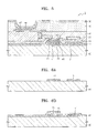
- FIG. 1 is a schematic cross-sectional view of an embodiment of an organic light emitting display apparatus
- FIGS. 2A through 2F are schematic cross-sectional views showing an embodiment of a method of manufacturing the organic light emitting display apparatus of FIG. 1 ;
- FIG. 3 is a schematic cross-sectional view of another embodiment of an organic light emitting display apparatus
- FIGS. 4A and 4B are schematic cross-sectional views showing another embodiment of a method of manufacturing the organic light emitting display apparatus of FIG. 3 ;
- FIG. 5 is a schematic cross-sectional view of an organic light emitting display apparatus according to a comparative example.
- FIGS. 6A through 6G are schematic cross-sectional views showing a method of manufacturing the organic light emitting display apparatus of FIG. 5 , according to the comparative example.
- FIG. 1 is a schematic cross-sectional view of an embodiment of an organic light emitting display apparatus 1.
- FIGS. 2A through 2F are schematic cross-sectional views showing an embodiment of a method of manufacturing the organic light emitting display apparatus 1 of FIG. 1 .
- a pixel region PXL1 having a light emitting layer 119, a thin film transistor (TFT) region TFT1 having a TFT, and a capacitor region CAP 1 having a capacitor are formed on a substrate 10.
- the substrate 10 and a first protection layer 12 are formed.
- the substrate 10 may be formed of a transparent material
- the first protection layer 12 may be formed of an insulating film.
- a gate electrode 213 of the TFT is formed on the first protection layer 12.
- a first insulating layer 14 that functions as a gate insulating film is formed on the gate electrode 213, and a semiconductor layer 215 is formed on the first insulating layer 14.
- the semiconductor layer 215 includes a transparent conductive oxide.
- the transparent oxide may include at least one of gallium (Ga), indium (In), zinc (Zn), hafnium (Hf), and tin (Sn).
- the transparent conductive oxide may be one of InGaZnO, ZnSnO, InZnO, InGaO, ZnO, TiO, and hafnium-indium-zinc oxide (HIZO).
- An oxide semiconductor TFT that includes a transparent conductive oxide, as an active layer has high performance characteristics and can be manufactured using a low temperature process, and thus, is evaluated as an optimum device for a backplane for a flat panel display apparatus.
- the oxide semiconductor TFT has a transparent characteristic in a visible light region and is flexible. Therefore, the oxide semiconductor TFT may be applied to a transparent display apparatus or a flexible display apparatus.
- a second insulating layer 16 covering the semiconductor layer 215 is formed.
- Source and drain electrodes 217 connected to the semiconductor layer 215 through contact holes Cl that penetrate through the second insulating layer 16 are formed on the second insulating layer 16.
- One of the source and drain electrodes 217 is connected to an upper edge of a pixel electrode 111 of the pixel region PXL1 via a via hole C2 that simultaneously penetrates the first protection layer 12, the first insulating layer 14, and the second insulating layer 16.
- the pixel electrode 111 that includes a transparent conductive material is formed on the substrate 10 in the pixel region PXL1.
- the pixel electrode 111 may include at least one of indium tin oxide (ITO), indium zink oxide (IZO), zinc oxide (ZnO), indium oxide (In203), indium gallium oxide (IGO), and aluminum zinc oxide (AZO).
- the pixel electrode 111 may be formed as a multiple layer that includes a semi-transparent metal layer 111a that includes silver (Ag). As depicted in FIG. 1 , the pixel electrode 111 may further include the semi-transparent metal layer 111a that includes silver (Ag) and a layer 111b that includes a transparent conductive material such as ITO on the semi-transparent metal layer 111a.
- the semi-transparent metal layer 111a functions as a semi-transparent mirror and may form a resonance structure together with a facing electrode 120 that functions as a reflection mirror, and thus, can increase optical extraction efficiency of the display apparatus.
- the first protection layer 12 is formed above/on an upper edge of the pixel electrode 111 (i.e. on an edge of the pixel electrode 111 on a side of the pixel electrode 111 that faces away from the substrate).
- the first protection layer 12 may function as a protective film for preventing the pixel electrode 111 from degrading during a manufacturing process of the pixel electrode 111, and may function as a dielectric film of the capacitor.
- the first protection layer 12 may be one of various insulating films formed of a material selected from SiNx, SiOx, and SiON.
- a second protection layer 113 is formed above/on an upper edge of the pixel electrode 111 (i.e. on an edge of the pixel electrode 111 on a side of the pixel electrode 111 that faces away from the substrate) by using the same material used to form the gate electrode 213.
- the first insulating layer 14 and the second insulating layer 16 are sequentially stacked on the second protection layer 113.
- the second protection layer 113, the first insulating layer 14, and the second insulating layer 16 form an opening for exposing the pixel electrode 111.
- Etching surfaces S1 of the opening in the second protection layer 113, the first insulating layer 14, and the second insulating layer 16 form the same plane.
- the second protection layer 113 may function as a protective film for preventing the pixel electrode 111 from degrading during the manufacturing process of the pixel electrode 111.
- a third insulating layer 18 is formed on the second insulating layer 16, and an opening C4 that exposes the pixel electrode 11 1 is formed in the third insulating layer 18.
- Etching surfaces S2 of the third insulating layer 18 and the first protection layer 12 form the same plane. Accordingly, the etching surfaces S2 of the first protection layer 12 and the second protection layer 113 that expose the pixel electrode 111 may form a gap G.
- the light emitting layer 119 is formed on the pixel electrode 111, and light generated from the light emitting layer 119 is emitted towards the substrate 10 through the pixel electrode 111 formed of a transparent conductive material.
- the light emitting layer 119 may be formed of a low molecular organic material or a polymer organic material. If the light emitting layer 119 is formed of a low molecular organic material, a hole transport layer (HTL), a hole injection Layer (HIL), an electron transport layer (ETL), and an electron injection layer (EIL) may be stacked around the light emitting layer 119. Also, various layers may be stacked as necessary.
- the low molecular organic material may include copper phthalocyanine (CuPc), N,N'-di(naphthalene-l-yl)-N,N'-diphenyl-benzidinc (NPB), or tris-8-hydroxyquinoline aluminum (Alq3).
- a hole transport layer HTL may be included in addition to the light emitting layer 119.
- the HTL may be formed of poly-(2,4)-ethylene-dihydroxy thiophene (PEDOT) or polyaniline (PANI).
- the organic material may be a poly organic material such as polyphenylenevinylene (PPV), and polyfluorene.
- the facing electrode 120 as a common electrode is formed on the light emitting layer 119.
- the pixel electrode 111 is used as an anode, and the facing electrode 120 is used as a cathode.
- the polarities of the pixel electrode 111 and the facing electrode 120 may be reversed in other embodiments.
- the facing electrode 120 may be formed as a reflective electrode that includes a reflective material.
- the facing electrode 120 may include at least one of Al, Mg, Li, Ca, LiF/Ca, and LiF/Al. Since the facing electrode 120 is a reflective electrode, light generated from the light emitting layer 119 is reflected by the facing electrode 120 and is emitted towards the substrate 10 through the pixel electrode 111 formed of a transparent conductive material. If the pixel electrode 111 further includes the semi-transparent metal layer 111a that includes silver Ag, the semi-transparent metal layer 111a may function as a semi-transparent mirror, may form a resonance structure together with the facing electrode 120 that functions as a reflection mirror, thereby increasing optical extraction efficiency of the organic light emitting display apparatus 1.
- a capacitor first electrode 311 and a capacitor second electrode 313 are disposed on the substrate 10 with the first protection layer 12 interposed therebetween.
- the capacitor first electrode 311 is formed on the same layer as the pixel electrode 111 1 using the same material used to form the pixel electrode 111.
- the capacitor second electrode 313 is formed on the same layer as the gate electrode 213 using the same material used to form the gate electrode 213.
- the first protection layer 12 functions as a dielectric film. In some embodiments, since the capacitor first electrode 311 and the capacitor second electrode 313 are respectively formed in the same mask process for forming the pixel electrode 111 and the gate electrode 213, the manufacturing process may be simplified.
- the first insulating layer 14 and the second insulating layer 16 are sequentially stacked on the capacitor second electrode 313, and a capacitor third electrode 317 that is formed on the same layer as the source and drain electrodes 217.
- the capacitor 317 may be formed of the same material used to form the source and drain electrodes 217, and may be formed on the second insulating layer 16. Since the capacitor first electrode 311 and the capacitor second electrode 313 form a metal-insulator-metal (MIM) cap, when the area of the capacitor is increased to increase a capacitance, an opening ratio of a display apparatus may be reduced. However, when the capacitor third electrode 317 is additionally formed, the capacitance is increased since the capacitor third electrode 317 is connected in parallel to the capacitor first electrode 311 and the capacitor second electrode 313. Therefore, even though the area of the capacitor is reduced, the reduced capacitance can be compensated for.
- MIM metal-insulator-metal
- FIGS. 2A through 2F are schematic cross-sectional views showing an embodiment of a method of manufacturing the organic light emitting display apparatus 1 of FIG. 1 .
- the pixel electrode 111 and the capacitor first electrode 311 are simultaneously formed on the substrate 10 in a first mask process.
- a buffer layer (not shown) that includes Si0 2 and/or SiNx may further be formed on the substrate 10 to provide planarity to the substrate 10 and to block penetration of foreign elements into the substrate 10.
- FIG. 2A shows a result whereby, after depositing a transparent conductive material on the substrate and coating a photoresist (not shown) on the transparent conductive material, the pixel electrode 111 and the capacitor first electrode 311 are simultaneously patterned by a photolithography process using a first mask (not shown).
- the first mask process using photolithography includes a series of processes such as developing, etching, and stripping or ashing after exposing the first mask (not shown) using an exposure apparatus (not shown).
- the same mask processes using photolithography will not be repeatedly described.
- FIG. 2B is a cross-sectional view of a result of a second mask process of the embodiment of an organic light emitting display apparatus 1.
- the first protection layer 12 is formed on the resultant product of the first mask process, and the second protection layer 113, the gate electrode 213, and the capacitor second electrode 313 are simultaneously formed on the first protection layer 12.
- the second protection layer 113 is not formed in a region where the via hole C2 contacts the pixel electrode 111. Accordingly, the second protection layer 113 has an area smaller than that of the pixel electrode 111.
- FIG. 2C is a cross-sectional view of a resultant product of a third mask process of the embodiment of an organic light emitting display apparatus 1 .
- the first insulating layer 14 is formed on the resultant product of the second mask process, and the semiconductor layer 215 is formed on the first insulating layer 14.
- the semiconductor layer 215 may include a transparent conductive oxide.
- FIG. 2D is a cross-sectional view of a resultant product of a fourth mask process of the embodiment of an organic light emitting display apparatus 1.
- the second insulating layer 16 is formed on the resultant product of the third mask process, and the contact hole C 1 and the via hole C2 are formed.
- an opening C3 that exposes an upper surface of the second protection layer 113 is formed by removing the first insulating layer 14 and the second insulating layer 16. Since the second protection layer 113 is not removed but remains above the pixel electrode 111, the second protection layer 113 protects the first protection layer 12 and the pixel electrode 111 when the contact hole C1, the via hole C2, and the opening C3 are formed.
- FIG. 2E is a cross-sectional view of a resultant product of a fifth mask process of the embodiment of an organic light emitting display apparatus 1 .
- the source and drain electrodes 217 and the capacitor third electrode 317 are formed by patterning the metal material.
- the metal material for forming the source and drain electrodes 217 is also deposited on the opening C3 that is formed in the fourth mask process.
- the metal material is removed together with the second protection layer 113.
- the second protection layer 113 and the metal material are removed by a single etching process. If the second protection layer 113 is formed of a material different from that used to form the source and drain electrodes 217, multiple etching processes may be performed.
- the first protection layer 12 protects the pixel electrode 111.
- FIG. 2F is a cross-sectional view of a resultant product of a sixth mask process of the embodiment of an organic light emitting display apparatus 1.
- the third insulating layer 18 is formed on the resultant product of the fifth mask process, and the opening C4 that exposes an upper surface of the pixel electrode 111 is formed by removing a portion of the third insulating layer 18.
- the first protection layer 12 formed on the pixel electrode 111 is also removed. Accordingly, the third insulating layer 18 and the first protection layer 12 may form the same etching surface S2.
- FIG. 3 is a schematic cross-sectional view of another embodiment of an organic light emitting display apparatus 2.
- FIGS. 4A and 4B are schematic cross-sectional views showing an embodiment of a method of manufacturing the organic light emitting display apparatus 2 of FIG. 3 .
- mainly the differences from the organic light emitting display apparatus 1 will be described.
- FIGS. 4A and 4B are schematic cross-sectional views respectively showing the fifth and sixth mask processes of the organic light emitting display apparatus 2.
- the first through fourth mask processes of the organic light emitting display apparatus 2 are performed the same as described with reference to the organic light emitting display apparatus 1 of FIG. 1 .
- the source and drain electrodes 217 and the capacitor third electrode 317 are formed by patterning the metal material.
- the metal material for forming the source and drain electrodes 217 is also deposited in the opening C3 in the fourth mask process.
- the metal material in the opening C3 is removed together with the second protection layer 113 and the first protection layer 12. Accordingly, since the second protection layer 113 and the first protection layer 12 are etched in the same mask process, the second protection layer 113 and the first protection layer 12 have the same etching surface S3.
- the third insulating layer 18 is formed on the resultant product of the fifth mask process, and the opening C4 that exposes the upper surface of the pixel electrode 111 is formed by removing a portion of the third insulating layer 18.
- the first protection layer 12 since the first protection layer 12 is removed together with the second protection layer 113 in the fifth mask process, the first protection layer 12 and the second protection layer 113 have the same etching surface S3.
- FIG. 5 is a schematic cross-sectional view of an organic light emitting display apparatus 3 according to a comparative example.
- FIGS. 6A through 6G are schematic cross-sectional views showing a method of manufacturing the comparative example of an organic light emitting display apparatus 3 of FIG. 5 .
- FIG. 6A is a schematic cross-sectional view of a result of a first mask process of the organic light emitting display apparatus 3. Referring to FIG. 6A , a gate electrode 41 and a capacitor first electrode 51 of a TFT are simultaneously formed on a substrate 40 in the first mask process.
- FIG. 6B is a schematic cross-sectional view of a result of a second mask process of the organic light emitting display apparatus 3.
- a first insulating layer 42 is formed on the resultant product of the first mask process, and a semiconductor layer 43 that includes a transparent conductive oxide is formed on the first insulating layer 42.
- FIG. 6C is a schematic cross-sectional view of a result of a third mask process of the organic light emitting display apparatus 3.
- a second insulating layer 44 is formed on the resultant product of the second mask process, and contact holes C5 that expose portions of the semiconductor layer 43 are formed.
- FIG. 6D is a schematic cross-sectional view of a result of a fourth mask process of the organic light emitting display apparatus 3.
- the source and drain electrodes 45 are formed by patterning the material.
- a capacitor third electrode 55 is also simultaneously formed.
- FIG. 6E is a schematic cross-sectional view of a result of a fifth mask process of the organic light emitting display apparatus 3.
- a third insulating layer 46 is formed on the resultant product of the fourth mask process, and a via hole C6 that exposes one of the source and drain electrodes 45 is formed.
- FIG. 6F is a schematic cross-sectional view of a result of a sixth mask process of the organic light emitting display apparatus 3.
- the pixel electrode 47 is formed by patterning the material.
- FIG. 6G is a schematic cross-sectional view of a result of a seventh mask process of the organic light emitting display apparatus 3.
- a fourth insulating layer 48 is formed on the resultant product of the sixth mask process, and an opening C7 that exposes an upper surface of the pixel electrode 47 is formed by removing a portion of the fourth insulating layer 48.
- a light emitting layer 49 and a facing electrode 50 are formed in the opening C7 formed in the seventh mask process.
- Embodiments of the present invention are described with reference to an organic light emitting display apparatus, but the present invention is not limited thereto.
- the present invention may also be applied to a liquid crystal display apparatus in which a light emitting layer includes liquid crystals.
- the present invention may also be applied to various kinds of display apparatuses.
Landscapes
- Physics & Mathematics (AREA)
- Engineering & Computer Science (AREA)
- Nonlinear Science (AREA)
- Microelectronics & Electronic Packaging (AREA)
- Crystallography & Structural Chemistry (AREA)
- Chemical & Material Sciences (AREA)
- Mathematical Physics (AREA)
- General Physics & Mathematics (AREA)
- Optics & Photonics (AREA)
- Power Engineering (AREA)
- Geometry (AREA)
- Manufacturing & Machinery (AREA)
- Electroluminescent Light Sources (AREA)
- Devices For Indicating Variable Information By Combining Individual Elements (AREA)
Applications Claiming Priority (1)
| Application Number | Priority Date | Filing Date | Title |
|---|---|---|---|
| KR1020110047944A KR20120129592A (ko) | 2011-05-20 | 2011-05-20 | 평판 표시 장치용 백플레인, 이를 포함하는 평판 표시 장치, 및 그 제조 방법 |
Publications (2)
| Publication Number | Publication Date |
|---|---|
| EP2525405A2 true EP2525405A2 (fr) | 2012-11-21 |
| EP2525405A3 EP2525405A3 (fr) | 2014-08-27 |
Family
ID=46062157
Family Applications (1)
| Application Number | Title | Priority Date | Filing Date |
|---|---|---|---|
| EP12168449.2A Withdrawn EP2525405A3 (fr) | 2011-05-20 | 2012-05-17 | Fond de panier pour appareil d'affichage à panneau plat, appareil d'affichage à écran plat et procédé de fabrication de la face arrière |
Country Status (6)
| Country | Link |
|---|---|
| US (2) | US8618546B2 (fr) |
| EP (1) | EP2525405A3 (fr) |
| JP (1) | JP6054629B2 (fr) |
| KR (1) | KR20120129592A (fr) |
| CN (1) | CN102842582B (fr) |
| TW (1) | TWI529948B (fr) |
Cited By (2)
| Publication number | Priority date | Publication date | Assignee | Title |
|---|---|---|---|---|
| WO2016170355A1 (fr) * | 2015-04-22 | 2016-10-27 | Flexenable Limited | Composant de commande pour support optique entraîné par un courant |
| US11605655B2 (en) | 2014-02-27 | 2023-03-14 | Semiconductor Energy Laboratory Co., Ltd. | Semiconductor device, and module and electronic appliance including the same |
Families Citing this family (23)
| Publication number | Priority date | Publication date | Assignee | Title |
|---|---|---|---|---|
| KR20120129592A (ko) * | 2011-05-20 | 2012-11-28 | 삼성디스플레이 주식회사 | 평판 표시 장치용 백플레인, 이를 포함하는 평판 표시 장치, 및 그 제조 방법 |
| KR102021028B1 (ko) * | 2012-12-04 | 2019-09-16 | 삼성디스플레이 주식회사 | 유기 발광 표시 장치 |
| KR102015873B1 (ko) * | 2013-01-03 | 2019-10-22 | 삼성디스플레이 주식회사 | 표시장치용 백플레인 및 그의 제조 방법 |
| JP5948427B2 (ja) * | 2013-03-18 | 2016-07-06 | パナソニック株式会社 | 薄膜半導体基板、発光パネル及び薄膜半導体基板の製造方法 |
| TWI502784B (zh) * | 2013-03-21 | 2015-10-01 | Chunghwa Picture Tubes Ltd | 電致發光裝置之電極基板的製作方法以及電致發光裝置的製作方法 |
| KR102049443B1 (ko) * | 2013-05-15 | 2019-11-28 | 삼성디스플레이 주식회사 | 유기 발광 표시 장치 및 그 제조 방법 |
| KR102116493B1 (ko) * | 2013-05-23 | 2020-06-08 | 삼성디스플레이 주식회사 | 유기발광표시장치 및 이의 제조방법 |
| KR102093458B1 (ko) | 2013-07-05 | 2020-03-26 | 삼성디스플레이 주식회사 | 커패시터 |
| JP6169005B2 (ja) * | 2014-01-17 | 2017-07-26 | 株式会社ジャパンディスプレイ | 発光素子表示装置 |
| US20150349000A1 (en) * | 2014-05-29 | 2015-12-03 | Qualcomm Mems Technologies, Inc. | Fabrication of transistor with high density storage capacitor |
| KR102236381B1 (ko) | 2014-07-18 | 2021-04-06 | 삼성디스플레이 주식회사 | 유기 발광 표시 장치 및 유기 발광 표시 장치의 제조 방법 |
| CN104157613B (zh) * | 2014-07-31 | 2017-03-08 | 京东方科技集团股份有限公司 | 一种阵列基板的制备方法 |
| TWI582968B (zh) | 2014-08-15 | 2017-05-11 | 群創光電股份有限公司 | 陣列基板結構及接觸結構 |
| US9766517B2 (en) * | 2014-09-05 | 2017-09-19 | Semiconductor Energy Laboratory Co., Ltd. | Display device and display module |
| KR102360783B1 (ko) | 2014-09-16 | 2022-02-10 | 삼성디스플레이 주식회사 | 디스플레이 장치 |
| KR102284756B1 (ko) | 2014-09-23 | 2021-08-03 | 삼성디스플레이 주식회사 | 디스플레이 장치 |
| KR102460407B1 (ko) * | 2015-10-30 | 2022-10-27 | 엘지디스플레이 주식회사 | 유기 발광 표시 장치 및 그의 제조방법 |
| KR102581258B1 (ko) * | 2016-06-10 | 2023-09-22 | 삼성디스플레이 주식회사 | 유기발광표시장치 및 유기발광표시장치의 제조방법 |
| CN107579083B (zh) * | 2017-09-30 | 2024-06-11 | 京东方科技集团股份有限公司 | 阵列基板及制备方法和显示装置 |
| CN107887398B (zh) * | 2017-11-14 | 2022-01-21 | 京东方科技集团股份有限公司 | 阵列基板及其制备方法、显示面板以及显示装置 |
| KR102503168B1 (ko) * | 2018-02-08 | 2023-02-27 | 삼성디스플레이 주식회사 | 표시 장치 및 그의 제조 방법 |
| KR20240117936A (ko) * | 2023-01-26 | 2024-08-02 | 엘지디스플레이 주식회사 | 표시 장치 |
| KR20240176890A (ko) * | 2023-06-16 | 2024-12-26 | 삼성디스플레이 주식회사 | 표시 장치 및 이의 제조 방법 |
Family Cites Families (35)
| Publication number | Priority date | Publication date | Assignee | Title |
|---|---|---|---|---|
| US4528480A (en) * | 1981-12-28 | 1985-07-09 | Nippon Telegraph & Telephone | AC Drive type electroluminescent display device |
| JP4030193B2 (ja) * | 1998-07-16 | 2008-01-09 | 株式会社半導体エネルギー研究所 | 半導体装置の作製方法 |
| TWI232595B (en) * | 1999-06-04 | 2005-05-11 | Semiconductor Energy Lab | Electroluminescence display device and electronic device |
| KR100395755B1 (ko) * | 2001-06-28 | 2003-08-21 | 삼성전자주식회사 | 비휘발성 메모리 소자 및 그 제조방법 |
| TWI270919B (en) * | 2002-04-15 | 2007-01-11 | Semiconductor Energy Lab | Display device and method of fabricating the same |
| JP2004192935A (ja) * | 2002-12-11 | 2004-07-08 | Hitachi Displays Ltd | 有機el表示装置 |
| KR100521272B1 (ko) * | 2002-12-20 | 2005-10-12 | 삼성에스디아이 주식회사 | 휘도가 개선된 유기전계 발광표시장치 |
| KR100557730B1 (ko) * | 2003-12-26 | 2006-03-06 | 엘지.필립스 엘시디 주식회사 | 듀얼패널타입 유기전계발광 소자 및 그 제조방법 |
| US8629819B2 (en) * | 2005-07-14 | 2014-01-14 | Semiconductor Energy Laboratory Co., Ltd. | Semiconductor device and driving method thereof |
| JP5132097B2 (ja) * | 2005-07-14 | 2013-01-30 | 株式会社半導体エネルギー研究所 | 表示装置 |
| JP5060738B2 (ja) * | 2006-04-28 | 2012-10-31 | 株式会社ジャパンディスプレイイースト | 画像表示装置 |
| KR20080058762A (ko) | 2006-12-22 | 2008-06-26 | 엘지디스플레이 주식회사 | 박막트랜지스터 액정표시장치용 어레이 기판 및 그제조방법 |
| JP5275608B2 (ja) * | 2007-10-19 | 2013-08-28 | 株式会社半導体エネルギー研究所 | 半導体基板の作製方法 |
| KR100964227B1 (ko) * | 2008-05-06 | 2010-06-17 | 삼성모바일디스플레이주식회사 | 평판 표시 장치용 박막 트랜지스터 어레이 기판, 이를포함하는 유기 발광 표시 장치, 및 이들의 제조 방법 |
| CN102047426B (zh) * | 2008-05-29 | 2013-02-06 | 夏普株式会社 | 半导体装置及其制造方法 |
| KR101545923B1 (ko) | 2008-11-26 | 2015-08-21 | 엘지디스플레이 주식회사 | 산화물 박막 트랜지스터 및 그 제조방법 |
| KR101251725B1 (ko) * | 2008-12-18 | 2013-04-05 | 파나소닉 주식회사 | 유기 일렉트로 루미네슨스 표시 장치 및 그 제조 방법 |
| US8441007B2 (en) * | 2008-12-25 | 2013-05-14 | Semiconductor Energy Laboratory Co., Ltd. | Display device and manufacturing method thereof |
| JP2010177223A (ja) * | 2009-01-27 | 2010-08-12 | Videocon Global Ltd | 液晶表示装置及びその製造方法 |
| KR101074788B1 (ko) * | 2009-01-30 | 2011-10-20 | 삼성모바일디스플레이주식회사 | 평판 표시 장치 및 이의 제조 방법 |
| JP2010204239A (ja) * | 2009-03-02 | 2010-09-16 | Seiko Epson Corp | 液晶装置および電子機器 |
| KR101050461B1 (ko) * | 2009-04-23 | 2011-07-19 | 삼성모바일디스플레이주식회사 | 유기 발광 디스플레이 장치 및 유기 발광 디스플레이 장치의 제조방법 |
| KR101646808B1 (ko) * | 2009-10-28 | 2016-08-08 | 가부시키가이샤 제이올레드 | 렌즈 시트, 표시 패널 장치 및 표시 장치 |
| KR101093424B1 (ko) * | 2009-11-10 | 2011-12-14 | 삼성모바일디스플레이주식회사 | 유기전계발광 표시 장치 및 그의 제조 방법 |
| KR101117642B1 (ko) * | 2009-11-16 | 2012-03-05 | 삼성모바일디스플레이주식회사 | 유기 발광 표시 장치 및 그 제조 방법 |
| KR101108176B1 (ko) * | 2010-07-07 | 2012-01-31 | 삼성모바일디스플레이주식회사 | 더블 게이트형 박막 트랜지스터 및 이를 구비한 유기 발광 표시 장치 |
| JP5574456B2 (ja) * | 2010-08-06 | 2014-08-20 | パナソニック株式会社 | 発光素子とその製造方法、および発光装置 |
| KR101764272B1 (ko) * | 2010-12-02 | 2017-08-16 | 삼성디스플레이 주식회사 | 유기 발광 표시 장치 및 그 제조방법 |
| KR20120129592A (ko) * | 2011-05-20 | 2012-11-28 | 삼성디스플레이 주식회사 | 평판 표시 장치용 백플레인, 이를 포함하는 평판 표시 장치, 및 그 제조 방법 |
| KR101873448B1 (ko) * | 2011-07-15 | 2018-07-03 | 삼성디스플레이 주식회사 | 유기발광표시장치 및 이의 제조방법 |
| KR101801350B1 (ko) * | 2011-08-01 | 2017-12-21 | 삼성디스플레이 주식회사 | 박막 트랜지스터 어레이 기판, 이를 포함하는 유기 발광 표시 장치 및 그 제조 방법 |
| KR101810051B1 (ko) * | 2011-08-09 | 2017-12-19 | 삼성디스플레이 주식회사 | 유기 발광 표시 장치 및 그 제조방법 |
| KR102080009B1 (ko) * | 2013-05-29 | 2020-04-08 | 삼성디스플레이 주식회사 | 유기 발광 표시 장치 및 그 제조방법 |
| CN103928470B (zh) * | 2013-06-24 | 2017-06-13 | 上海天马微电子有限公司 | 一种氧化物半导体tft阵列基板及其制造方法 |
| KR20150000949A (ko) * | 2013-06-25 | 2015-01-06 | 삼성디스플레이 주식회사 | 표시 장치 및 이의 제조 방법 |
-
2011
- 2011-05-20 KR KR1020110047944A patent/KR20120129592A/ko not_active Abandoned
-
2012
- 2012-04-11 US US13/444,736 patent/US8618546B2/en active Active
- 2012-05-10 TW TW101116699A patent/TWI529948B/zh active
- 2012-05-16 JP JP2012112741A patent/JP6054629B2/ja active Active
- 2012-05-17 EP EP12168449.2A patent/EP2525405A3/fr not_active Withdrawn
- 2012-05-21 CN CN201210158797.9A patent/CN102842582B/zh active Active
-
2013
- 2013-11-20 US US14/085,211 patent/US9048257B2/en active Active
Non-Patent Citations (1)
| Title |
|---|
| None |
Cited By (4)
| Publication number | Priority date | Publication date | Assignee | Title |
|---|---|---|---|---|
| US11605655B2 (en) | 2014-02-27 | 2023-03-14 | Semiconductor Energy Laboratory Co., Ltd. | Semiconductor device, and module and electronic appliance including the same |
| US11916088B2 (en) | 2014-02-27 | 2024-02-27 | Semiconductor Energy Laboratory Co., Ltd. | Semiconductor device, and module and electronic appliance including the same |
| WO2016170355A1 (fr) * | 2015-04-22 | 2016-10-27 | Flexenable Limited | Composant de commande pour support optique entraîné par un courant |
| US10971062B2 (en) | 2015-04-22 | 2021-04-06 | Flexenable Limited | Control component for a current-driven optical media |
Also Published As
| Publication number | Publication date |
|---|---|
| TW201248865A (en) | 2012-12-01 |
| EP2525405A3 (fr) | 2014-08-27 |
| US8618546B2 (en) | 2013-12-31 |
| CN102842582B (zh) | 2016-09-07 |
| KR20120129592A (ko) | 2012-11-28 |
| US20120292612A1 (en) | 2012-11-22 |
| US20140080270A1 (en) | 2014-03-20 |
| JP6054629B2 (ja) | 2016-12-27 |
| CN102842582A (zh) | 2012-12-26 |
| TWI529948B (zh) | 2016-04-11 |
| JP2012242834A (ja) | 2012-12-10 |
| US9048257B2 (en) | 2015-06-02 |
Similar Documents
| Publication | Publication Date | Title |
|---|---|---|
| US9048257B2 (en) | Backplane for flat panel display apparatus, flat panel display apparatus, and method of manufacturing the backplane | |
| US9502604B2 (en) | Backplane for flat panel display apparatus, method of manufacturing the backplane, and organic light emitting display apparatus including the backplane | |
| US8575606B2 (en) | Back panel for flat panel display apparatus, flat panel display apparatus comprising the same, and method of manufacturing the back panel | |
| KR101833235B1 (ko) | 박막 트랜지스터 어레이 기판, 이를 포함하는 유기 발광 표시 장치 및 그 제조 방법 | |
| US8785937B2 (en) | Organic light-emitting display apparatus and method of manufacturing the same | |
| US8637868B2 (en) | Thin-film transistor array substrate, organic light emitting display device including the same, and method of manufacturing the same | |
| KR101881895B1 (ko) | 박막트랜지스터 어레이 기판, 이를 포함하는 유기 발광 표시 장치 및 박막트랜지스터 어레이 기판의 제조 방법 | |
| US9123594B2 (en) | Organic light-emitting display apparatus having high aperture ratio | |
| KR101890799B1 (ko) | 박막 트랜지스터 어레이 기판, 이를 포함하는 유기 발광 표시 장치 및 그 제조 방법 | |
| KR101938761B1 (ko) | 박막 트랜지스터 어레이 기판, 이를 포함하는 유기 발광 표시 장치 및 그 제조 방법 | |
| US20130037783A1 (en) | Organic light-emitting display apparatus and method of manufacturing the same | |
| KR20130007310A (ko) | 유기 발광 소자, 유기 발광 표시 장치 및 그 제조 방법 | |
| KR20160081100A (ko) | 유기 발광 표시 장치의 제조 방법 및 상기 제조 방법에 의해 제조된 유기 발광 표시 장치 | |
| KR102124044B1 (ko) | 박막 트랜지스터 기판, 그 제조방법 및 이를 포함하는 유기 발광 디스플레이 장치 | |
| KR101944916B1 (ko) | 박막 트랜지스터 어레이 기판, 이를 포함하는 유기 발광 표시 장치 및 그 제조 방법 | |
| KR20140125181A (ko) | 평판표시장치용 백플레인 및 그의 제조방법 |
Legal Events
| Date | Code | Title | Description |
|---|---|---|---|
| PUAI | Public reference made under article 153(3) epc to a published international application that has entered the european phase |
Free format text: ORIGINAL CODE: 0009012 |
|
| AK | Designated contracting states |
Kind code of ref document: A2 Designated state(s): AL AT BE BG CH CY CZ DE DK EE ES FI FR GB GR HR HU IE IS IT LI LT LU LV MC MK MT NL NO PL PT RO RS SE SI SK SM TR |
|
| AX | Request for extension of the european patent |
Extension state: BA ME |
|
| 17P | Request for examination filed |
Effective date: 20140331 |
|
| RBV | Designated contracting states (corrected) |
Designated state(s): AL AT BE BG CH CY CZ DE DK EE ES FI FR GB GR HR HU IE IS IT LI LT LU LV MC MK MT NL NO PL PT RO RS SE SI SK SM TR |
|
| PUAL | Search report despatched |
Free format text: ORIGINAL CODE: 0009013 |
|
| AK | Designated contracting states |
Kind code of ref document: A3 Designated state(s): AL AT BE BG CH CY CZ DE DK EE ES FI FR GB GR HR HU IE IS IT LI LT LU LV MC MK MT NL NO PL PT RO RS SE SI SK SM TR |
|
| AX | Request for extension of the european patent |
Extension state: BA ME |
|
| RIC1 | Information provided on ipc code assigned before grant |
Ipc: H01L 27/12 20060101AFI20140722BHEP Ipc: H01L 29/66 20060101ALI20140722BHEP |
|
| RAP1 | Party data changed (applicant data changed or rights of an application transferred) |
Owner name: SAMSUNG DISPLAY CO., LTD. |
|
| STAA | Information on the status of an ep patent application or granted ep patent |
Free format text: STATUS: THE APPLICATION HAS BEEN WITHDRAWN |
|
| 18W | Application withdrawn |
Effective date: 20170823 |