EP2525407A2 - Nitrid-Halbleiterbauelement, Nitrid-Halbleiterwafer und Verfahren zur Herstellung einer Nitrid-Halbleiterschicht - Google Patents
Nitrid-Halbleiterbauelement, Nitrid-Halbleiterwafer und Verfahren zur Herstellung einer Nitrid-Halbleiterschicht Download PDFInfo
- Publication number
- EP2525407A2 EP2525407A2 EP12152936A EP12152936A EP2525407A2 EP 2525407 A2 EP2525407 A2 EP 2525407A2 EP 12152936 A EP12152936 A EP 12152936A EP 12152936 A EP12152936 A EP 12152936A EP 2525407 A2 EP2525407 A2 EP 2525407A2
- Authority
- EP
- European Patent Office
- Prior art keywords
- concentration
- layer
- foundation
- less
- thickness
- Prior art date
- Legal status (The legal status is an assumption and is not a legal conclusion. Google has not performed a legal analysis and makes no representation as to the accuracy of the status listed.)
- Granted
Links
Images






Classifications
-
- H—ELECTRICITY
- H10—SEMICONDUCTOR DEVICES; ELECTRIC SOLID-STATE DEVICES NOT OTHERWISE PROVIDED FOR
- H10H—INORGANIC LIGHT-EMITTING SEMICONDUCTOR DEVICES HAVING POTENTIAL BARRIERS
- H10H20/00—Individual inorganic light-emitting semiconductor devices having potential barriers, e.g. light-emitting diodes [LED]
- H10H20/80—Constructional details
- H10H20/81—Bodies
- H10H20/822—Materials of the light-emitting regions
- H10H20/824—Materials of the light-emitting regions comprising only Group III-V materials, e.g. GaP
- H10H20/825—Materials of the light-emitting regions comprising only Group III-V materials, e.g. GaP containing nitrogen, e.g. GaN
-
- H—ELECTRICITY
- H10—SEMICONDUCTOR DEVICES; ELECTRIC SOLID-STATE DEVICES NOT OTHERWISE PROVIDED FOR
- H10D—INORGANIC ELECTRIC SEMICONDUCTOR DEVICES
- H10D62/00—Semiconductor bodies, or regions thereof, of devices having potential barriers
- H10D62/80—Semiconductor bodies, or regions thereof, of devices having potential barriers characterised by the materials
- H10D62/85—Semiconductor bodies, or regions thereof, of devices having potential barriers characterised by the materials being Group III-V materials, e.g. GaAs
- H10D62/8503—Nitride Group III-V materials, e.g. AlN or GaN
-
- H—ELECTRICITY
- H10—SEMICONDUCTOR DEVICES; ELECTRIC SOLID-STATE DEVICES NOT OTHERWISE PROVIDED FOR
- H10P—GENERIC PROCESSES OR APPARATUS FOR THE MANUFACTURE OR TREATMENT OF DEVICES COVERED BY CLASS H10
- H10P14/00—Formation of materials, e.g. in the shape of layers or pillars
- H10P14/20—Formation of materials, e.g. in the shape of layers or pillars of semiconductor materials
- H10P14/29—Formation of materials, e.g. in the shape of layers or pillars of semiconductor materials characterised by the substrates
- H10P14/2901—Materials
- H10P14/2902—Materials being Group IVA materials
- H10P14/2905—Silicon, silicon germanium or germanium
-
- H—ELECTRICITY
- H10—SEMICONDUCTOR DEVICES; ELECTRIC SOLID-STATE DEVICES NOT OTHERWISE PROVIDED FOR
- H10P—GENERIC PROCESSES OR APPARATUS FOR THE MANUFACTURE OR TREATMENT OF DEVICES COVERED BY CLASS H10
- H10P14/00—Formation of materials, e.g. in the shape of layers or pillars
- H10P14/20—Formation of materials, e.g. in the shape of layers or pillars of semiconductor materials
- H10P14/32—Formation of materials, e.g. in the shape of layers or pillars of semiconductor materials characterised by intermediate layers between substrates and deposited layers
- H10P14/3202—Materials thereof
- H10P14/3214—Materials thereof being Group IIIA-VA semiconductors
- H10P14/3216—Nitrides
-
- H—ELECTRICITY
- H10—SEMICONDUCTOR DEVICES; ELECTRIC SOLID-STATE DEVICES NOT OTHERWISE PROVIDED FOR
- H10P—GENERIC PROCESSES OR APPARATUS FOR THE MANUFACTURE OR TREATMENT OF DEVICES COVERED BY CLASS H10
- H10P14/00—Formation of materials, e.g. in the shape of layers or pillars
- H10P14/20—Formation of materials, e.g. in the shape of layers or pillars of semiconductor materials
- H10P14/32—Formation of materials, e.g. in the shape of layers or pillars of semiconductor materials characterised by intermediate layers between substrates and deposited layers
- H10P14/3242—Structure
- H10P14/3244—Layer structure
- H10P14/3251—Layer structure consisting of three or more layers
- H10P14/3252—Alternating layers, e.g. superlattice
-
- H—ELECTRICITY
- H10—SEMICONDUCTOR DEVICES; ELECTRIC SOLID-STATE DEVICES NOT OTHERWISE PROVIDED FOR
- H10P—GENERIC PROCESSES OR APPARATUS FOR THE MANUFACTURE OR TREATMENT OF DEVICES COVERED BY CLASS H10
- H10P14/00—Formation of materials, e.g. in the shape of layers or pillars
- H10P14/20—Formation of materials, e.g. in the shape of layers or pillars of semiconductor materials
- H10P14/34—Deposited materials, e.g. layers
- H10P14/3402—Deposited materials, e.g. layers characterised by the chemical composition
- H10P14/3414—Deposited materials, e.g. layers characterised by the chemical composition being group IIIA-VIA materials
- H10P14/3416—Nitrides
-
- H—ELECTRICITY
- H10—SEMICONDUCTOR DEVICES; ELECTRIC SOLID-STATE DEVICES NOT OTHERWISE PROVIDED FOR
- H10P—GENERIC PROCESSES OR APPARATUS FOR THE MANUFACTURE OR TREATMENT OF DEVICES COVERED BY CLASS H10
- H10P14/00—Formation of materials, e.g. in the shape of layers or pillars
- H10P14/20—Formation of materials, e.g. in the shape of layers or pillars of semiconductor materials
- H10P14/34—Deposited materials, e.g. layers
- H10P14/3438—Doping during depositing
- H10P14/3441—Conductivity type
- H10P14/3442—N-type
-
- H—ELECTRICITY
- H10—SEMICONDUCTOR DEVICES; ELECTRIC SOLID-STATE DEVICES NOT OTHERWISE PROVIDED FOR
- H10P—GENERIC PROCESSES OR APPARATUS FOR THE MANUFACTURE OR TREATMENT OF DEVICES COVERED BY CLASS H10
- H10P14/00—Formation of materials, e.g. in the shape of layers or pillars
- H10P14/20—Formation of materials, e.g. in the shape of layers or pillars of semiconductor materials
- H10P14/34—Deposited materials, e.g. layers
- H10P14/3438—Doping during depositing
- H10P14/3448—Delta-doping
-
- H—ELECTRICITY
- H10—SEMICONDUCTOR DEVICES; ELECTRIC SOLID-STATE DEVICES NOT OTHERWISE PROVIDED FOR
- H10H—INORGANIC LIGHT-EMITTING SEMICONDUCTOR DEVICES HAVING POTENTIAL BARRIERS
- H10H20/00—Individual inorganic light-emitting semiconductor devices having potential barriers, e.g. light-emitting diodes [LED]
- H10H20/01—Manufacture or treatment
- H10H20/011—Manufacture or treatment of bodies, e.g. forming semiconductor layers
- H10H20/013—Manufacture or treatment of bodies, e.g. forming semiconductor layers having light-emitting regions comprising only Group III-V materials
- H10H20/0133—Manufacture or treatment of bodies, e.g. forming semiconductor layers having light-emitting regions comprising only Group III-V materials with a substrate not being Group III-V materials
- H10H20/01335—Manufacture or treatment of bodies, e.g. forming semiconductor layers having light-emitting regions comprising only Group III-V materials with a substrate not being Group III-V materials the light-emitting regions comprising nitride materials
-
- H—ELECTRICITY
- H10—SEMICONDUCTOR DEVICES; ELECTRIC SOLID-STATE DEVICES NOT OTHERWISE PROVIDED FOR
- H10H—INORGANIC LIGHT-EMITTING SEMICONDUCTOR DEVICES HAVING POTENTIAL BARRIERS
- H10H20/00—Individual inorganic light-emitting semiconductor devices having potential barriers, e.g. light-emitting diodes [LED]
- H10H20/80—Constructional details
- H10H20/81—Bodies
- H10H20/815—Bodies having stress relaxation structures, e.g. buffer layers
Definitions
- Embodiments described herein relate generally to a nitride semiconductor device, a nitride semiconductor wafer, and a method for manufacturing a nitride semiconductor layer.
- LED Light emitting diodes
- nitride semiconductors semiconductor light emitting devices using nitride semiconductors
- Electronic devices using the nitride semiconductors have been used for highfrequency devices and high-power devices.
- nitride semiconductor device When such nitride semiconductor device is formed on a silicon (Si) substrate having an excellent mass productivity, a defect and a crack are easily generated due to a difference in lattice constant or thermal expansion coefficient. There is a demand for a technique of producing a high-quality crystal on the silicon substrate. Especially when it is attempted to form a thick n-type GaN layer on the silicon substrate, a crack tends to be generated.
- a nitride semiconductor device includes: a stacked foundation layer, and a functional layer.
- the stacked foundation layer is formed on an AIN buffer layer formed on a silicon substrate.
- the stacked foundation layer includes a plurality of AIN foundation layers and a plurality of GaN foundation layers being alternately stacked with the AIN foundation layers.
- the functional layer includes a low-concentration part, and a high-concentration part.
- the low-concentration part is provided on the stacked foundation layer.
- the low-concentration part includes a nitride semiconductor and has a Si concentration less than 1 X 10 18 cm -3 .
- the high-concentration part is provided on the low-concentration part and has a Si concentration not less than 1 X 10 18 cm -3 .
- a substrate-side GaN foundation layer closest to the silicon substrate among the plurality of GaN foundation layers includes a first portion, a second portion, and a third portion.
- the first portion has a Si concentration less than 5 X 10 18 cm -3 .
- the second portion has a Si concentration less than 5 X 10 18 cm -3 .
- the third portion is provided between the first portion and the second portion.
- the third portion has a Si concentration not less than 5 X 10 18 cm -3 and has a thickness smaller than a sum of a thickness of the first portion and a thickness of the second portion.
- a nitride semiconductor device includes: a functional layer formed on an AIN buffer layer formed on a silicon substrate.
- the functional layer includes: a plurality of low-concentration parts, and a plurality of high-concentration parts.
- the plurality of low-concentration parts include a nitride semiconductor and have a Si concentration less than 5 X 10 18 cm -3 .
- the plurality of high-concentration parts have a Si concentration not less than 5 X 10 18 cm -3 .
- the low-concentration parts are alternately stacked with the high-concentration parts. A thickness of each of the high-concentration parts is smaller than a thickness of each of the low-concentration parts.
- a nitride semiconductor wafer includes: a silicon substrate, an AIN buffer layer, a stacked foundation layer, and a functional layer.
- the AIN buffer layer is provided on the silicon substrate.
- the stacked foundation layer is provided on the AIN buffer layer.
- the stacked foundation layer includes a plurality of AIN foundation layers and a plurality of GaN foundation layers being alternately stacked with the AIN foundation layers.
- the functional layer includes a low-concentration part, and a high-concentration part.
- the low-concentration part is provided on the stacked foundation layer.
- the low-concentration part includes a nitride semiconductor and has a Si concentration less than 5 X 10 18 cm -3 .
- the high-concentration part is provided on the low-concentration part and has a Si concentration not less than 5 X 10 18 cm -3 .
- a substrate-side GaN foundation layer closest to the silicon substrate among the plurality of GaN foundation layers includes: a first portion, a second portion, and a third portion.
- the first portion has a Si concentration less than 5 X 10 18 cm -3 .
- the second portion has a Si concentration less than 5 X 10 18 cm -3 .
- the third portion is provided between the first portion and the second portion.
- the third portion has a Si concentration not less than 5 X 10 18 cm -3 and has a thickness smaller than a sum of a thickness of the first portion and a thickness of the second portion.
- a nitride semiconductor wafer includes: a silicon substrate, an AIN buffer layer, and a functional layer.
- the AIN buffer layer is provided on the silicon substrate.
- the functional layer is provided on the AlN buffer layer.
- the functional layer includes a plurality of low-concentration parts, and a plurality of high-concentration parts.
- the plurality of low-concentration parts include a nitride semiconductor and have a Si concentration less than 5 X 10 18 cm -3 .
- the plurality of high-concentration parts have a Si concentration not less than 5 X 10 18 cm -3 .
- the low-concentration parts are alternately stacked with the high-concentration parts. A thickness of each of the high-concentration parts is smaller than a thickness of each of the low-concentration parts.
- a method for manufacturing a nitride semiconductor layer can form a stacked foundation layer by alternately stacking a plurality of AIN foundation layers and a plurality of GaN foundation layers on an AIN buffer layer provided on a silicon substrate.
- the method can form a functional layer by forming a low-concentration part on the stacked foundation layer and forming a high-concentration part on the low-concentration part.
- the low-concentration part includes a nitride semiconductor and has a Si concentration less than 5 X 10 18 cm -3 .
- the high-concentration part has a Si concentration not less than 5 X 10 18 cm -3 .
- Forming a substrate-side GaN foundation layer closest to the silicon substrate among the plurality of GaN foundation layers including forming a first portion, a second low-concentration foundation, and a third portion.
- the first portion has a Si concentration less than 5 X 10 18 cm -3 .
- the second portion has a Si concentration less than 5 X 10 18 cm -3 .
- the third portion is provided between the first portion and the second portion.
- the third portion has a Si concentration not less than 5 X 10 18 cm -3 and has a thickness smaller than a sum of a thickness of the first portion and a thickness of the second portion.
- a method for manufacturing a nitride semiconductor layer can form a functional layer on an AIN buffer layer formed on a silicon substrate.
- the forming the functional layer includes repeating a process a plurality of times.
- the process includes forming a low-concentration part and forming a high-concentration part.
- the low-concentration part includes a nitride semiconductor and has a Si concentration less than 5 X 10 18 cm -3 .
- the high-concentration part has a Si concentration not less than 5 X 10 18 cm -3 .
- a thickness of each of the high-concentration parts is smaller than a thickness of each of the low-concentration parts.
- the embodiment relates to a nitride semiconductor device.
- the nitride semiconductor device according to the embodiment includes semiconductor devices such as semiconductor light emitting devices, semiconductor light receiving devices and electronic devices.
- semiconductor light emitting devices include light emitting diodes (LEDs) and laser diodes (LDs).
- semiconductor light receiving devices include photodiodes (PDs).
- the electronic devices include high electron mobility transistors (HEMTs), heterojunction bipolar transistors (HBTs), field-effect transistors (FETs) and Schottky barrier diodes (SBDs).
- HEMTs high electron mobility transistors
- HBTs heterojunction bipolar transistors
- FETs field-effect transistors
- SBDs Schottky barrier diodes
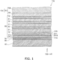
- FIG. 1 is a schematic sectional view illustrating configuration of a nitride semiconductor device according to the first embodiment.
- a nitride semiconductor device 110 As shown in FIG. 1 , a nitride semiconductor device 110 according to the embodiment has a stacked foundation layer 50 and a functional layer 10s.
- the stacked foundation layer 50 is formed on an AIN buffer layer 55 formed on a silicon substrate 40.
- the thickness of the AIN buffer layer 55 is, for example, about 30 nanometers (nm).
- an intermediate layer 54 is provided between the stacked foundation layer 50 and the AIN buffer layer 55.
- an AlGaN layer is used as the intermediate layer 54.
- an Al 0.25 Ga 0.75 N layer is used as the intermediate layer 54.
- the thickness of the intermediate layer 54 is, for example, about 40 nm.
- the intermediate layer 54 is provided as needed and may be omitted according to circumstances.
- the stacked foundation layer 50 includes a plurality of AIN foundation layers 52 and a plurality of GaN foundation layers 51 alternately stacked with the AIN foundation layers 52.
- the functional layer 10s is provided on the stacked foundation layer 50.
- a direction heading from the stacked foundation layer 50 toward the functional layer 10s is defined as a Z-axis direction.
- One axis perpendicular to the Z axis is defined as an X axis.
- a direction perpendicular to the Z axis and the X axis is defined as a Y axis.
- the functional layer 10s is stacked with the stacked foundation layer 50 along the Z axis.
- a term of "stacked” includes the case where layers are stacked in contact with each other as well as the case where layers are stacked with another layer being interposed therebetween.
- a phrase of "provided on” includes the case where layers are provided in contact with each other as well as the case where layers are provided with another layer being interposed therebetween.
- the functional layer 10s includes a low-concentration part 10l and a high-concentration part 10h.
- the low-concentration part 10l includes a nitride semiconductor and has a Si concentration less than 1 X 10 18 cm -3 .
- the low-concentration part 10l has a Si concentration less than 1 X 10 17 cm -3 .
- the Si concentration of the low-concentration part 10l is not more than a detection limit in a secondary ion mass spectrometory (SIMS) measurement generally used.
- SIMS secondary ion mass spectrometory
- an undoped GaN layer is used as the low-concentration part 10l.
- the high-concentration part 10h is provided on the low-concentration part 10l.
- the high-concentration part 10h is stacked on the low-concentration part 10l along the Z axis.
- the high-concentration part 10h has a Si concentration not less than 1 X 10 18 cm -3 .
- an n-type GaN layer is used as the high-concentration part 10h.
- the high-concentration part 10h is included in an n-type semiconductor layer 10.
- the n-type semiconductor layer 10 includes the low-concentration part 10l.
- each of the plurality of AIN foundation layers 52 is, for example, a low-temperature AIN layer formed at low temperature.
- the thickness of each of the AIN foundation layers 52 is, for example, about 12 nm.
- the thickness of each of the GaN foundation layers 51 is, for example, about 300 nm.
- each of the number of the GaN foundation layers 51 and the number of the AIN foundation layers 52 (that is, the number of pairs) is three. However, the embodiment is not limited to this, and any number of pairs may be employed.
- the GaN foundation layer 51 closest to the silicon substrate 40 among the plurality of GaN foundation layers 51 is defined as a substrate-side GaN foundation layer 51s.
- the substrate-side GaN foundation layer 51s incudes a first portion 51 a, a second portion 51b and a third portion 51c.
- the third portion 51c is provided between the first portion 51a and the second portion 51b.
- the first portion 51a, the third portion 51c and the second portion 51b are stacked along the Z axis in this order.
- the Si concentration of the first portion 51a and the second portion 51b is less than 5 X 10 18 cm -3 .
- the Si concentration of the third portion 51c is not less than 5 X 10 18 cm -3 .
- the Si concentration of the third portion 51c is not more than 1 X 10 21 cm -3 .
- the thickness of the third portion 51c (length along the Z axis) is smaller than a sum of the thickness of the first portion 51a and the thickness of the second portion 51b.
- the third portion 51c may contain silicon nitride (its composition ratio is optional), that is, Si ⁇ N ⁇ (0 ⁇ ⁇ , 0 ⁇ ⁇ ).
- the thickness of the third portion 51c is not less than 0.1 nm and not more than 50 nm.
- the third portion 51c is, for example, a ⁇ -doped layer 51d.
- the silicon substrate 40 is, for example, a Si (111) substrate.
- the plane direction of the silicon substrate 40 is not necessarily a (111) plane.
- nitride semiconductor device 110 is a light emitting device
- FIG. 2 is a schematic sectional view illustrating configuration of a nitride semiconductor device according to the first embodiment.
- the functional layer 10s further includes a light emitting part 30 and a p-type semiconductor layer 20.
- the light emitting part 30 is provided on the n-type semiconductor layer 10 (the high-concentration part 10h).
- the p-type semiconductor layer 20 is provided on the light emitting part 30.
- the p-type semiconductor layer 20 includes a nitride semiconductor.
- the p-type semiconductor layer 20 includes at least one of Mg, Zn and C.
- FIG. 3 is a schematic sectional view illustrating configuration of a part of the nitride semiconductor device according to the first embodiment.
- the light emitting part 30 includes a plurality of barrier layers 31 and a plurality of well layers 32 each provided between the barrier layers 31.
- the plurality of barrier layers 31 and the plurality of well layers 32 alternately stacked with the barrier layers 31 along the Z axis.
- the well layer 32 contains, for example, In x1 Ga 1-x1 N (0 ⁇ x1 ⁇ 1).
- the barrier layer 31 contains, for example, GaN. In other words, for example, the well layer 32 contains In and the barrier layer 31 does not substantially contain In. Bandgap energy in the barrier layer 31 is larger than bandgap energy in the well layer 32.
- the light emitting part 30 may have Single Quantum Well (SQW) structure. At this time, the light emitting part 30 includes the two barrier layers 31 and the well layer 32 provided between the barrier layers 31. Alternatively, the light emitting part 30 may have Multi Quantum Well (MQW) structure. At this time, the light emitting part 30 includes the three or more barrier layers 31 and the well layers 32 each provided between the barrier layers 31.
- SQL Single Quantum Well
- MQW Multi Quantum Well
- the light emitting part 30 includes the (n + 1) barrier layers 31 and the n well layers 32 ("n" is an integer of 2 or more).
- the (i + 1) th barrier layer BL(i + 1) is disposed between the i lh barrier layer BLi and the p-type semiconductor layer 20 ("i" is an integer that is not less than 1 and not more than (n-1)).
- the (i + 1) th well layer WL(i + 1) is disposed between the i th well layer WLi and the p-type semiconductor layer 20.
- the first barrier layer BL1 is provided between the n-type semiconductor layer 10 and the first well layer WL1.
- the n th well layer WLn is provided between the n th barrier layer BLn and the (n + 1) th barrier layer BL(n + 1).
- the (n + 1) th barrier layer BL(n + 1) is provided between the n th well layer WLn and the p-type semiconductor layer 20.
- the peak wavelength of light (emitted light) emitted from the light emitting part 30 is, for example, not less than 200 nanometers (nm) and not more than 1600 nm. However, in the embodiment, the peak wavelength is optional.
- the Si ⁇ -doped layer 51d (the third portion 51c) is provided in the substrate-side GaN foundation layer 51s closest to the silicon substrate 40 among the plurality of GaN foundation layers 51. Thereby, it is possible to provide the high-quality nitride semiconductor device with reduced number of cracks formed on the silicon substrate.
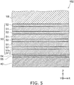
- FIG. 4 to FIG. 7 are schematic sectional views illustrating configuration of first to fourth samples, respectively.
- FIG. 4 shows the configuration of the first sample 151 corresponding to the embodiment.
- the Si ⁇ -doped layer 51 d (the third portion 51c) is provided in the substrate-side GaN foundation layer 51s closest to the silicon substrate 40 among the plurality of GaN foundation layers 51.
- no high-concentration part 10h is provided in the first sample 151.
- the first sample 151 is in the state before the high-concentration part 10h is provided on the low-concentration part 10l in the configuration of the embodiment.
- no ⁇ -doped layer 51 d (the third portion 51c) is provided in all of the plurality of GaN foundation layers 51.
- the ⁇ -doped layer 51d (the third portion 51c) is provided on the upper side of the AIN foundation layer 52 and in contact with the AIN foundation layer 52.
- no ⁇ -doped layer 51 d (the third portion 51c) is provided in all of the plurality of GaN foundation layers 51.
- the ⁇ -doped layer 51d (the third portion 51c) is provided in the low-concentration part 10l.
- the first sample 151 was fabricated by a following fabrication method.
- an MOVPE Metal-Organic Vapor Phase Epitaxy
- MOVPE Metal-Organic Vapor Phase Epitaxy
- the Si(111) silicon substrate 40 was cleaned by using a mixed solution of H 2 O 2 and H 2 SO 4 (1:1) for 13 minutes.
- the silicon substrate 40 was cleaned by using 2% HF for 10 minutes. After cleaning, the silicon substrate 40 was introduced into an MOVPE reactor.
- the temperature of a susceptor was increased to 720°C under hydrogen atmosphere and TMA was supplied for eight seconds. Then, NH 3 was further supplied to form an AIN layer having a thickness of 30 nm serving as the AIN buffer layer 55.
- the temperature of the susceptor was increased to 1030°C to form an Al 0.25 Ga 0.75 N layer having a thickness of 40 nm serving as the intermediate layer 54.
- the temperature of the susceptor was increased to 1080°C to form a GaN layer having a thickness of 150 nm serving as a part (the first portion 51a) of the substrate-side GaN foundation layer 51 s. Then, supply of gas was interrupted and only SiH 4 and NH 3 were supplied for 300 seconds to form the Si ⁇ -doped layer 51 d.
- a GaN layer having a thickness of 150 nm was formed as a part (the second portion 51b) of the substrate-side GaN foundation layer 51 s.
- the temperature of the susceptor was decreased to 800°C to form a low-temperature AIN layer having a thickness of 12 nm serving as the AIN foundation layer 52.
- the temperature of the susceptor was increased to 1120°C to form a GaN layer having a thickness of 300 nm serving as the GaN foundation layer 51. Furthermore, growth of the above-mentioned AIN foundation layer 52 and GaN foundation layer 51 was repeated three times. Thereby, the stacked foundation layer 50 was formed.
- the second sample 152 was obtained.
- the third sample 153 was obtained.
- the fourth sample 154 was obtained.
- the ⁇ -doped layer 51 d is provided at a position away from the uppermost AIN foundation layer 52 by 300 nm.
- the above-mentioned first sample 151 to the fourth sample 154 were observed by using a Nomarski microscope.
- FIG. 8A to FIG. 8D are Nomarski microscope images illustrating characteristics of the first to fourth samples.
- the first sample 151 a surface without crack was obtained.
- a rocking curve of the wafer was measured by using an X-ray diffractometer.
- the full width at half maximum of a (002) plane was 364 arcseconds and the full width at half maximum of a (101) plane was 817 arcseconds.
- the full width at half maximum of the (002) plane is highly correlated to screw dislocation density and the full width at half maximum of the (101) plane is highly correlated to edge dislocation density.
- the first sample 151 has a low defect density.
- the second sample 152 has a higher defect density than the first sample.
- the crack CR was observed.
- the full width at half maximum of the (002) plane was 364 arcseconds and the full width at half maximum of the (101) plane was 999 arcseconds.
- the third sample 153 has the crack CR and characteristics of the semiconductor device formed on the wafer are poor. It is considered that, in the case where the ⁇ -doped layer 51d is provided in a region within 100 nm from the low-temperature AIN layer, the effect of reducing the dislocation by the ⁇ -doped layer 51d is obtained, the effect of applying the compressive strain due to formation of the GaN foundation layers 51 thereon cannot be brought about.
- the generation of the crack CR is suppressed.
- defect density is low.
- the thickness of the low-concentration part 10l and the thickness of the high-concentration part 10h are appropriately adjusted from viewpoints of the generation of crack and defect.
- the AIN foundation layer 52 does not match in lattice with the GaN foundation layer 51 located immediately therebelow. As a result, the strain is relaxed and the AIN foundation layer 52 has a lattice constant of AIN which is not affected by the influence of the strain.
- the GaN foundation layer 51 so as to grow pseudomorphically on the AIN foundation layer 52, GaN grows while being subjected to compressive strain. This results in a convex warp.
- the warp further protruding upwards can be made large.
- tensile strain which is applied in decreasing temperature after crystal growth due to difference between thermal expansion coefficients of Si and GaN, can be compensated. This promotes suppression of the generation of crack.
- GaN foundation layers 51 can terminate defects such as threading dislocation due to lattice mismatching between the silicon substrate 40 and the nitride semiconductor layer. Thereby, extending of detects to the functional layer 10s can be suppressed. As a result, with the embodiment, the high-performance device can be achieved.
- dislocation extending in the stacking direction (the Z-axis direction) is curved.
- dislocation in the functional layer 10s can be reduced.
- GaN grows in three-dimensional way in further forming the GaN foundation layers 51 on the ⁇ -doped layer 51d, compressive strain protruding upwards tends to be generated during crystal growth, thereby the generation of crack can easily suppressed.
- the thickness of the GaN foundation layer 51 be not less than 50 nm and not more than 1000 nm.
- the thickness is smaller than 50 nm, the effect of reducing dislocation such as threading dislocation generated between the silicon substrate 40 and the stacked foundation layer 50 is insufficient.
- the thickness is larger than 1000 nm, crack caused by tensile strain in decreasing temperature after crystal growth tends to be generated.
- the thickness of the GaN foundation layer 51 be not less than 15 nm and not more than 100 nm.
- the thickness is smaller than 15 nm, the effect of reducing dislocation is insufficient.
- the thickness is larger than 100 nm, crack caused by tensile strain tends to be generated.
- the thickness of the AIN foundation layers 52 (the low-temperature AIN layer) be, for example, not less than 5 nm and not more than 20 nm. It is noted that the crystal growth temperature of the AIN foundation layer 52 be, for example, not less than 600°C and not more than 1050°C. By setting the thickness and the temperature in these ranges, the lattice of the AIN foundation layer 52 is easily relaxed. Thereby, in forming the AIN foundation layer 52, it becomes hard to be subject to tensile strain from the GaN foundation layers 51 serving as a foundation. As a result, it is possible to efficiently form the lattice constant of AIN that is not affected by strain from the GaN foundation layers 51 serving as a foundation.
- the thickness of the AlN foundation layers 52 is smaller than 5 nm, it is difficult that AIN is sufficiently relaxed.
- the thickness of the AIN foundation layer 52 is larger than 20 nm, dislocation due to lattice relaxation increases.
- the formation temperature of the AIN foundation layers 52 is lower than 600°C, impurities are easily incorporated and furthermore, cubic crystal AIN grows, causing excessive generation of crystal dislocation.
- the formation temperature of the AIN foundation layer 52 is higher than 1050°C, strain is not relaxed and thus, tensile strain is easily introduced into the silicon substrate 40. Furthermore, since compressive strain cannot be appropriately applied during crystal growth of the GaN foundation layer 51, crack tends to be generated in decreasing temperature after crystal growth.
- the distance between the AIN foundation layers 52 (that is, the thickness of the GaN foundation layer 51) be not less the 50 nm and not more than 1000 nm.
- the GaN foundation layer 51 In forming the GaN foundation layer 51 on the AlN foundation layer 52, the GaN foundation layer 51 having a thickness not less than 50 nm and not more than 200 nm grows pseudomorphically on AIN foundation layer 52 and is tend to be subjected to compressive strain. Accordingly, when the distance between the AIN foundation layers 52 is larger than 1000 nm, the effect of applying compressive strain is insufficient. When the distance is smaller than 50 nm, the number of AIN foundation layers 52 in the GaN foundation layer 51 becomes excessively many and therefore, the temperature increase and decrease process is excessively repeated, decreasing the material use efficiency of the crystal growth apparatus and the like.
- the ⁇ -doped layer 51d contains Si with a concentration not less than 5 X 10 18 cm -3 and not more than 1 X 10 22 cm -3 mainly in GaN.
- the ⁇ -doped layer 51d may contain SiN.
- SiN may be partially formed in the plane. It is noted that the thickness of the ⁇ -doped layer 51d be not less than 0.1 nm and not more than 50 nm.
- the Si concentration is not less than 5 X 10 18 cm -3 and not more than 1 X 10 22 cm -3 , the GaN foundation layer 51 formed on the ⁇ -doped layer 51d tends to grow in a three-dimensional way. Thereby, it becomes easy to apply compressive strain, resulting in that the effect of suppressing the generation of crack is easily obtained.
- dislocation and crack in the functional layer 10s are reduced. Further, crystallinity of the functional layer 10s is improved. That is, the functional layer 10s has high quality.
- the ⁇ -doped layer 51d be provided in the substrate-side GaN foundation layer 51s.
- the ⁇ -doped layer 51d be provided in the substrate-side GaN foundation layer 51s.
- no ⁇ -doped layer 51d be provided in all of the GaN foundation layers 51 except for the substrate-side GaN foundation layer 51s among the plurality of GaN foundation layers 51.
- all of the GaN foundation layers 51 except for the substrate-side GaN foundation layer 51 s have the Si concentration less than 5 X 10 18 cm -3 .
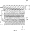
- FIG. 9 is a schematic sectional view illustrating configuration of another nitride semiconductor device according to the first embodiment.
- the functional layer 10s includes a plurality of low-concentration parts 10l and a plurality of high-concentration parts 10h.
- the thickness of each of the plurality of high-concentration parts 10h is smaller than the thickness of each of the low-concentration parts 10l.
- the plurality of low-concentration parts 10l and the plurality of high-concentration parts 10h are alternately disposed. In other words, the plurality of low-concentration parts 10l and the plurality of high-concentration parts 10h are alternately stacked along the Z axis.
- each of the high-concentration parts 10h is a Si ⁇ -doped layer 10d.
- Other configuration of the nitride semiconductor device 120 is the same as that of the nitride semiconductor device 110 and thus, description thereof is omitted.
- n-type semiconductor layer 10 is ⁇ -doped with Si.
- the thickness of each of the plurality of high-concentration parts 10h is not less than 0.1 nm and not more than 50 nm.
- the distance between the plurality of high-concentration parts 10h (the ⁇ -doped layers 10d), that is, the thickness of each of the plurality of low-concentration parts 10l, is not less than 300 nm and not more than 500 nm.
- the thickness of the n-type semiconductor layer 10 is, for example, 2.1 ⁇ m.
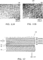
- FIG. 10 is a schematic sectional view illustrating configuration of a fifth sample of the nitride semiconductor device.
- the n-type semiconductor layer 10 is provided directly on the stacked foundation layer 50. Also in this case, the thickness of the n-type semiconductor layer 10 is, for example, 2.1 ⁇ m.
- no ⁇ -doped layer 10d is provided in the n-type semiconductor layer 10. That is, Si is doped in a wide region along the Z axis of the n-type semiconductor layer 10.
- FIG. 11A and FIG. 11B are Nomarski microscope images illustrating characteristics of the nitride semiconductor device.
- the thickness of the Si-doped GaN layer is not less than 1.5 ⁇ m, crack density tends to become very high. Accordingly, when the embodiment is applied to formation of the n-type GaN layer having a thickness not less than 1.5 ⁇ m, the effect of suppressing the generation of the crack CR can be effectively obtained.
- the nitride semiconductor device 120 is used as at least a part of the n-type semiconductor layer 10 such as the light emitting diode and the laser diode to produce a larger effect.
- the thickness of the n-type semiconductor layer 10 is generally not less than 2 ⁇ m. If the thickness of the n-type semiconductor layer 10 in such semiconductor light emitting device is not more than 1.5 ⁇ m, current spreading is insufficient, and thus, for example, in-plane light emission pattern becomes nonuniform. In addition, this disadvantageously leads to high resistance.
- crack density is reduced by providing the ⁇ -doped layer 51d in the stacked foundation layer 50. It is considered that, like the AlN foundation layer 52 (the low-temperature AlN layer), the GaN foundation layer 51 grown on the ⁇ -doped layer 51d is subjected to compressive strain and warp protruding upwards is previously stored during crystal growth to compensate tensile strain due to difference between thermal expansion coefficients of the GaN foundation layer 51 and the Si substrate in decreasing temperature after crystal growth
- the generation of the crack CR can be suppressed.
- the generation of the crack CR can be suppressed.
- the GaN layer in which the ⁇ -doped layers 10d are periodically provided becomes the n-type semiconductor layer 10.
- the bandgap energy of AIN (6.3 eV) is much larger than the bandgap energy of GaN (3.4 eV)
- the current flow is interrupt and it cannot function as an n-type GaN layer.
- the configuration of the embodiment is constructed. Thereby, it is possible to provide the wafer having a high-quality nitride semiconductor crystal formed on the Si substrate.
- the stacked foundation layer 50 is provided.
- the stacked foundation layer 50 is not necessarily provided.
- arbitral structure that applies compressive strain during growth may be provided between the functional layer 10s and the AIN buffer layer 55.
- an AlN/GaN superlattice structure or a structure in which Al composition is inclined in a stepped manner or continuously may be provided between the functional layer 10s and the AIN buffer layer 55.
- the semiconductor light emitting device may further include the stacked foundation layer 50 formed on the AIN buffer layer 55 and under the functional layer 10s.
- the stacked foundation layer 50 includes the plurality of AIN foundation layers 52 and the plurality of GaN foundation layers 51 alternately stacked with the AIN foundation layers 52.
- the substrate-side GaN foundation layer 51 s closest to the silicon substrate 40 among the plurality of GaN foundation layers 51 can have the first portion 51a having a Si concentration less than 5 X 10 18 cm -3 , the second portion 51b having a Si concentration less than 5 X 10 18 cm -3 and the third portion 51c that is provided between the first portion 51a and the second portion 51b, has a Si concentration not less than 5 X 10 18 cm -3 and has a thickness smaller than a sum of the thickness of the first portion 51a and the thickness of the second portion 51b.
- FIG. 12 is a schematic sectional view illustrating configuration of another nitride semiconductor device according to the first embodiment.
- another nitride semiconductor device 130 includes the functional layer 10s formed on the AlN buffer layer 55 formed on the silicon substrate 40.
- the intermediate layer 54 is provided on the AIN buffer layer 55 and the functional layer 10s is provided on the intermediate layer 54.
- the intermediate layer 54 is provided as needed and may be omitted according to circumstances.
- the functional layer 10s includes the plurality of low-concentration parts 10l and the plurality of high-concentration parts 10h (for example, ⁇ -doped layer 10d) alternately stacked with the low-concentration parts 10l.
- Each of the plurality of low-concentration parts 10l includes the nitride semiconductor and has a Si concentration less than 5 X 10 18 cm -3 .
- Each of the plurality of high-concentration parts 10h has a Si concentration not less than 5 X 10 18 cm -3 .
- the thickness of each of the plurality of high-concentration parts 10h is smaller than the thickness of each of the low-concentration parts 10l.
- the distance (for example, a period) between the ⁇ -doped layers 10d in the functional layer 10s be not less than 50 nm and not more than 500 nm.
- the distance is smaller than 50 nm, the doping concentration of the GaN layer becomes too high. The effect obtained by applying compressive strain cannot be sufficiently obtained.
- the distance (for example, period) is larger than 500 nm, it is noted that the number of ⁇ -doped layers 10d be not less than two and not more than 80.
- the part except for the ⁇ -doped layers 10d in the n-type semiconductor layer 10 may contain Si having a concentration not more than a half of the Si concentration in the ⁇ -doped layers 10d.
- the embodiment relates to a nitride semiconductor wafer.
- the wafer is provided with, for example, at least a part of the semiconductor devices, or a portion that becomes at least a part of the semiconductor devices.
- the semiconductor devices include the semiconductor light emitting device, the semiconductor light receiving device and the electronic device.
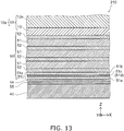
- FIG. 13 is a schematic sectional view illustrating configuration of the nitride semiconductor wafer according to the second embodiment.
- a nitride semiconductor wafer 210 includes the silicon substrate 40, the AIN buffer layer 55, the stacked foundation layer 50 and the functional layer 10s.
- the nitride semiconductor wafer 210 further includes the intermediate layer 54.
- the intermediate layer 54 may be omitted.
- the configuration described with respect to the first embodiment can be applied to each of the silicon substrate 40, the AIN buffer layer 55, the intermediate layer 54, the stacked foundation layer 50 and the functional layer 10s.
- the substrate-side GaN foundation layer 51s closest to the silicon substrate 40 among the plurality of GaN foundation layers 51s included in the stacked foundation layer 50 includes the first portion 51a having a Si concentration less than 5 X 10 18 cm -3 , the second portion 51b having a Si concentration less than 5 X 10 18 cm -3 and the third portion 51c that is provided between the first portion 51a and the second portion 51b.
- the third portion 51c has a Si concentration not less than 5 X 10 18 cm -3 and has a thickness smaller than the sum of the thickness of the first portion 51a and the thickness of the second portion 51b.
- FIG. 14 is a schematic sectional view illustrating configuration of another nitride semiconductor wafer according to the second embodiment.
- another nitride semiconductor wafer 230 includes the silicon substrate 40, the AIN buffer layer 55 provided on the silicon substrate 40 and the functional layer provided on the AIN buffer layer 55.
- the nitride semiconductor wafer 230 further includes the intermediate layer 54.
- the intermediate layer 54 may be omitted.
- the functional layer 10s includes the plurality of low-concentration parts 10l and the plurality of high-concentration parts 10h (for example, the ⁇ -doped layers 10d) alternately stacked with the low-concentration parts 10l.
- Each of the plurality of low-concentration parts 10l includes the nitride semiconductor and has a Si concentration less than 5 X 10 18 cm -3 .
- Each of the plurality of high-concentration parts 10h has a Si concentration not less than 5 X 10 18 cm -3 .
- the thickness of each of the plurality of high-concentration parts 10h is smaller than that of each of the low-concentration parts 10l.
- nitride semiconductor wafers 210 and 230 By using the nitride semiconductor wafers 210 and 230, it is possible to provide the nitride semiconductor wafer for the high-quality nitride semiconductor device with the reduced number of cracks formed on the silicon substrate.
- FIG. 15 is a flow chart illustrating a method for manufacturing the nitride semiconductor layer according to a third embodiment.
- the plurality of AIN foundation layers 52 and the plurality of GaN foundation layers 51 are alternately stacked on the AIN buffer layer 55 provided on the silicon substrate 40 to form the stacked foundation layer 50 (Step S110). Further, the low-concentration part 10l that includes the nitride semiconductor and has a Si concentration less than 5 X 10 18 cm -3 is formed on the stacked foundation layer 50 and the high-concentration part 10h having a Si concentration not less than 5 X 10 18 cm -3 is formed on the low-concentration part 10l to form the functional layer 10s (Step S120).
- Forming the stacked foundation layer 50 includes, in formation of the substrate-side GaN foundation layer 51s closest to the silicon substrate 40 among the plurality of GaN foundation layers 51, forming the first portion 51a having a Si concentration less than 5 X 10 18 cm -3 , the second portion 51b having a Si concentration less than 5 X 10 18 cm -3 and the third portion 51c that is provided between the first portion 51a and the second portion 51b, has a Si concentration not less than 5 X 10 18 cm -3 and has a thickness smaller than the sum of the thickness of the first portion 51a and the thickness of the second portion 51b.
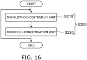
- FIG. 16 is a flow chart illustrating another method for manufacturing the nitride semiconductor layer according to the third embodiment.
- the manufacturing method includes a process of forming the functional layer 10s on the AIN buffer layer 55 formed on the silicon substrate 40 (Step S200).
- Forming the functional layer 10s repeats a process a plurality of times, the process including: forming a plurality of low-concentration parts 10l each including a nitride semiconductor and having a Si concentration less than 5 X 10 18 cm -3 (step S210); and forming a plurality of high-concentration parts 10h having a Si concentration not less than 5 X 10 18 cm -3 (step S220).
- the thickness of each of the plurality of high-concentration parts 10h is smaller than the thickness of each of the low-concentration parts 10l.
- MOCVD Metal-Organic Chemical Vapor Deposition
- MOVPE Metal-Organic Vapor Phase Epitaxy
- MBE Molecular Beam Epitaxy
- HVPE Hydride Vapor Phase Epitaxy
- TMGa trimethyl gallium
- TEGa triethyl gallium
- TMIn trimethyl indium
- TEIn triethyl indium
- TMAI trimethyl aluminum
- NH 3 ammonia
- MMHy monomethyl hydrazine
- DMHy dimethyl hydrazine
- SiH 4 monosilane
- Si 2 H 6 disilane
- the embodiment it is possible to provide a method for manufacturing a high-quality nitride semiconductor device with the reduced number of cracks formed on the silicon substrate, a nitride semiconductor wafer and a nitride semiconductor layer.
- nitride semiconductor includes all compositions of semiconductors of the chemical formula B x In y Al z Ga 1-x-y-z N (0 ⁇ x ⁇ 1, 0 ⁇ y ⁇ 1, 0 ⁇ z ⁇ 1, and x+y+z ⁇ 1) for which each of the compositional proportions x, y, and z are changed within the ranges.
- Nonride semiconductor further includes group V elements other than N (nitrogen) in the chemical formula recited above, various elements added to control various properties such as the conductivity type, etc., and various elements included unintentionally.
- perpendicular and parallel refer to not only strictly perpendicular and strictly parallel but also include, for example, the fluctuation due to manufacturing processes, etc. It is sufficient to be substantially perpendicular and substantially parallel.
- exemplary embodiments of the invention are described with reference to the specific examples. However, the invention is not limited to these specific examples.
- one skilled in the art may similarly practice the invention by appropriately selecting specific configurations of component included in substrates included in nitride semiconductor devices and wafers, AIN buffer layers, intermediate layers, stacked foundation layers, AIN foundation layers, GaN foundation layers, functional layers, semiconductor layers and light emitting parts, etc., from known art. Such practice is included in the scope of the invention to the extent that similar effects thereto are obtained.
- nitride semiconductor devices, nitride semiconductor wafers and methods for manufacturing nitride semiconductor layers practicable by an appropriate design modification by one skilled in the art based on the nitride semiconductor devices, nitride semiconductor wafers and methods for manufacturing nitride semiconductor layers described above as embodiments of the invention also are within the scope of the invention to the extent that the purport of the embodiments of the invention is included.
Landscapes
- Led Devices (AREA)
- Semiconductor Lasers (AREA)
- Chemical Vapour Deposition (AREA)
- Junction Field-Effect Transistors (AREA)
Applications Claiming Priority (1)
| Application Number | Priority Date | Filing Date | Title |
|---|---|---|---|
| JP2011109560A JP5023230B1 (ja) | 2011-05-16 | 2011-05-16 | 窒化物半導体素子、窒化物半導体ウェーハ及び窒化物半導体層の製造方法 |
Publications (3)
| Publication Number | Publication Date |
|---|---|
| EP2525407A2 true EP2525407A2 (de) | 2012-11-21 |
| EP2525407A3 EP2525407A3 (de) | 2015-11-25 |
| EP2525407B1 EP2525407B1 (de) | 2017-10-25 |
Family
ID=45655281
Family Applications (1)
| Application Number | Title | Priority Date | Filing Date |
|---|---|---|---|
| EP12152936.6A Active EP2525407B1 (de) | 2011-05-16 | 2012-01-27 | Nitrid-Halbleiterbauelement, Nitrid-Halbleiterwafer und Verfahren zur Herstellung einer Nitrid-Halbleiterschicht |
Country Status (5)
| Country | Link |
|---|---|
| US (1) | US8692287B2 (de) |
| EP (1) | EP2525407B1 (de) |
| JP (1) | JP5023230B1 (de) |
| KR (1) | KR101292470B1 (de) |
| CN (1) | CN102790147B (de) |
Cited By (1)
| Publication number | Priority date | Publication date | Assignee | Title |
|---|---|---|---|---|
| EP2736085A1 (de) * | 2012-11-21 | 2014-05-28 | Kabushiki Kaisha Toshiba | Nitrid-Halbleiterbauelement, Nitrid-Halbleiterwafer und Verfahren zur Herstellung einer Nitrid-Halbleiterschicht |
Families Citing this family (12)
| Publication number | Priority date | Publication date | Assignee | Title |
|---|---|---|---|---|
| JP5066274B1 (ja) * | 2011-05-16 | 2012-11-07 | 株式会社東芝 | 半導体発光素子 |
| JP5117609B1 (ja) | 2011-10-11 | 2013-01-16 | 株式会社東芝 | 窒化物半導体ウェーハ、窒化物半導体装置及び窒化物半導体結晶の成長方法 |
| JP5425284B1 (ja) | 2012-09-21 | 2014-02-26 | 株式会社東芝 | 半導体ウェーハ、半導体素子及び窒化物半導体層の製造方法 |
| KR101901932B1 (ko) * | 2012-11-02 | 2018-09-27 | 엘지전자 주식회사 | 이종 기판, 질화물 반도체 발광 소자 및 그 제조 방법 |
| JP6270536B2 (ja) * | 2013-06-27 | 2018-01-31 | 株式会社東芝 | 窒化物半導体素子、窒化物半導体ウェーハ及び窒化物半導体層の形成方法 |
| US11322643B2 (en) | 2014-05-27 | 2022-05-03 | Silanna UV Technologies Pte Ltd | Optoelectronic device |
| KR102318317B1 (ko) | 2014-05-27 | 2021-10-28 | 실라나 유브이 테크놀로지스 피티이 리미티드 | 반도체 구조물과 초격자를 사용하는 진보된 전자 디바이스 구조 |
| WO2015181656A1 (en) * | 2014-05-27 | 2015-12-03 | The Silanna Group Pty Limited | Electronic devices comprising n-type and p-type superlattices |
| WO2015181648A1 (en) | 2014-05-27 | 2015-12-03 | The Silanna Group Pty Limited | An optoelectronic device |
| JP6661330B2 (ja) | 2015-10-27 | 2020-03-11 | 株式会社ディスコ | Led基板の形成方法 |
| JP6652042B2 (ja) * | 2016-12-13 | 2020-02-19 | 三菱電機株式会社 | Iii−v族窒化物半導体エピタキシャルウェハの製造方法 |
| JP7158272B2 (ja) * | 2018-12-25 | 2022-10-21 | エア・ウォーター株式会社 | 化合物半導体基板 |
Family Cites Families (17)
| Publication number | Priority date | Publication date | Assignee | Title |
|---|---|---|---|---|
| JPH04301592A (ja) | 1991-03-29 | 1992-10-26 | Hitachi Ltd | 燃料集合体 |
| JP3744211B2 (ja) | 1997-09-01 | 2006-02-08 | 日亜化学工業株式会社 | 窒化物半導体素子 |
| JP4301592B2 (ja) | 1998-01-16 | 2009-07-22 | 三菱マテリアル株式会社 | 窒化物半導体層付き基板の製造方法 |
| CA2322490C (en) * | 1998-03-12 | 2010-10-26 | Nichia Chemical Industries, Ltd. | Nitride semiconductor device |
| JP3669848B2 (ja) | 1998-09-16 | 2005-07-13 | 日亜化学工業株式会社 | 窒化物半導体レーザ素子 |
| US6608330B1 (en) * | 1998-09-21 | 2003-08-19 | Nichia Corporation | Light emitting device |
| JP2003078169A (ja) | 1998-09-21 | 2003-03-14 | Nichia Chem Ind Ltd | 発光素子 |
| JP2001313421A (ja) | 2000-02-21 | 2001-11-09 | Sanken Electric Co Ltd | 半導体発光素子及びその製造方法 |
| JP2004047764A (ja) * | 2002-07-12 | 2004-02-12 | Hitachi Cable Ltd | 窒化物半導体の製造方法および半導体ウェハならびに半導体デバイス |
| TWI240969B (en) | 2003-06-06 | 2005-10-01 | Sanken Electric Co Ltd | Nitride semiconductor device and method for manufacturing same |
| JP2006114886A (ja) * | 2004-09-14 | 2006-04-27 | Showa Denko Kk | n型III族窒化物半導体積層構造体 |
| JP4622466B2 (ja) | 2004-11-12 | 2011-02-02 | 日亜化学工業株式会社 | 窒化物半導体素子 |
| KR100662191B1 (ko) | 2004-12-23 | 2006-12-27 | 엘지이노텍 주식회사 | 질화물 반도체 발광소자 및 그 제조방법 |
| JP2010509081A (ja) | 2006-11-10 | 2010-03-25 | エージェンシー フォー サイエンス, テクノロジー アンド リサーチ | マイクロメカニカル構造体およびマイクロメカニカル構造体の製造方法 |
| JP5471440B2 (ja) * | 2007-05-02 | 2014-04-16 | 豊田合成株式会社 | Iii族窒化物半導体発光素子の製造方法 |
| KR20090034169A (ko) * | 2007-10-02 | 2009-04-07 | 주식회사 에피밸리 | 3족 질화물 반도체 발광소자 |
| KR101017396B1 (ko) * | 2008-08-20 | 2011-02-28 | 서울옵토디바이스주식회사 | 변조도핑층을 갖는 발광 다이오드 |
-
2011
- 2011-05-16 JP JP2011109560A patent/JP5023230B1/ja active Active
- 2011-08-31 US US13/222,200 patent/US8692287B2/en active Active
-
2012
- 2012-01-19 CN CN201210017269.1A patent/CN102790147B/zh active Active
- 2012-01-27 EP EP12152936.6A patent/EP2525407B1/de active Active
- 2012-01-30 KR KR1020120008745A patent/KR101292470B1/ko active Active
Non-Patent Citations (1)
| Title |
|---|
| None |
Cited By (3)
| Publication number | Priority date | Publication date | Assignee | Title |
|---|---|---|---|---|
| EP2736085A1 (de) * | 2012-11-21 | 2014-05-28 | Kabushiki Kaisha Toshiba | Nitrid-Halbleiterbauelement, Nitrid-Halbleiterwafer und Verfahren zur Herstellung einer Nitrid-Halbleiterschicht |
| US9054036B2 (en) | 2012-11-21 | 2015-06-09 | Kabushiki Kaisha Toshiba | Nitride semiconductor device, nitride semiconductor wafer, and method for forming nitride semiconductor layer |
| US9673284B2 (en) | 2012-11-21 | 2017-06-06 | Kabushiki Kaisha Toshiba | Nitride semiconductor device, nitride semiconductor wafer, and method for forming nitride semiconductor layer |
Also Published As
| Publication number | Publication date |
|---|---|
| US8692287B2 (en) | 2014-04-08 |
| CN102790147A (zh) | 2012-11-21 |
| EP2525407A3 (de) | 2015-11-25 |
| US20120292593A1 (en) | 2012-11-22 |
| CN102790147B (zh) | 2015-05-06 |
| EP2525407B1 (de) | 2017-10-25 |
| KR20120128085A (ko) | 2012-11-26 |
| JP5023230B1 (ja) | 2012-09-12 |
| JP2012243807A (ja) | 2012-12-10 |
| KR101292470B1 (ko) | 2013-07-31 |
Similar Documents
| Publication | Publication Date | Title |
|---|---|---|
| EP2525407B1 (de) | Nitrid-Halbleiterbauelement, Nitrid-Halbleiterwafer und Verfahren zur Herstellung einer Nitrid-Halbleiterschicht | |
| US8969891B2 (en) | Nitride semiconductor device, nitride semiconductor wafer and method for manufacturing nitride semiconductor layer | |
| US10008571B2 (en) | Semiconductor wafer, semiconductor device, and method for manufacturing nitride semiconductor layer | |
| US20150001547A1 (en) | Nitride semiconductor element, nitride semiconductor wafer, and method for forming nitride semiconductor layer | |
| US9054036B2 (en) | Nitride semiconductor device, nitride semiconductor wafer, and method for forming nitride semiconductor layer | |
| US8975165B2 (en) | III-V semiconductor structures with diminished pit defects and methods for forming the same | |
| US9478706B2 (en) | Semiconductor light emitting device, nitride semiconductor wafer, and method for manufacturing nitride semiconductor layer | |
| US20160247968A1 (en) | Nitride semiconductor wafer, nitride semiconductor element, and method for manufacturing nitride semiconductor wafer | |
| US9397167B2 (en) | Nitride semiconductor wafer, nitride semiconductor device, and method for manufacturing nitride semiconductor wafer | |
| CN102790155B (zh) | 氮化物半导体器件和晶片以及制造氮化物半导体层的方法 | |
| US8779437B2 (en) | Wafer, crystal growth method, and semiconductor device | |
| JP6649693B2 (ja) | 窒化物半導体発光素子及びその製造方法 | |
| JP5337272B2 (ja) | 窒化物半導体素子、窒化物半導体ウェーハ及び窒化物半導体層の製造方法 | |
| KR20120128088A (ko) | 질화물 반도체 소자, 질화물 반도체 웨이퍼 및 질화물 반도체층의 제조 방법 | |
| JP5597663B2 (ja) | 半導体発光素子、窒化物半導体ウェーハ及び窒化物半導体層の製造方法 |
Legal Events
| Date | Code | Title | Description |
|---|---|---|---|
| PUAI | Public reference made under article 153(3) epc to a published international application that has entered the european phase |
Free format text: ORIGINAL CODE: 0009012 |
|
| 17P | Request for examination filed |
Effective date: 20120127 |
|
| AK | Designated contracting states |
Kind code of ref document: A2 Designated state(s): AL AT BE BG CH CY CZ DE DK EE ES FI FR GB GR HR HU IE IS IT LI LT LU LV MC MK MT NL NO PL PT RO RS SE SI SK SM TR |
|
| AX | Request for extension of the european patent |
Extension state: BA ME |
|
| PUAL | Search report despatched |
Free format text: ORIGINAL CODE: 0009013 |
|
| AK | Designated contracting states |
Kind code of ref document: A3 Designated state(s): AL AT BE BG CH CY CZ DE DK EE ES FI FR GB GR HR HU IE IS IT LI LT LU LV MC MK MT NL NO PL PT RO RS SE SI SK SM TR |
|
| AX | Request for extension of the european patent |
Extension state: BA ME |
|
| RIC1 | Information provided on ipc code assigned before grant |
Ipc: H01L 29/20 20060101AFI20151022BHEP Ipc: H01L 33/32 20100101ALI20151022BHEP Ipc: H01L 21/02 20060101ALI20151022BHEP Ipc: H01L 33/00 20100101ALI20151022BHEP |
|
| STAA | Information on the status of an ep patent application or granted ep patent |
Free format text: STATUS: EXAMINATION IS IN PROGRESS |
|
| 17Q | First examination report despatched |
Effective date: 20161104 |
|
| REG | Reference to a national code |
Ref country code: DE Ref legal event code: R079 Ref document number: 602012038837 Country of ref document: DE Free format text: PREVIOUS MAIN CLASS: H01L0029200000 Ipc: H01L0033120000 |
|
| GRAP | Despatch of communication of intention to grant a patent |
Free format text: ORIGINAL CODE: EPIDOSNIGR1 |
|
| STAA | Information on the status of an ep patent application or granted ep patent |
Free format text: STATUS: GRANT OF PATENT IS INTENDED |
|
| RIC1 | Information provided on ipc code assigned before grant |
Ipc: H01L 33/32 20100101ALI20170330BHEP Ipc: H01L 21/02 20060101ALI20170330BHEP Ipc: H01L 33/12 20100101AFI20170330BHEP Ipc: H01L 33/00 20100101ALI20170330BHEP |
|
| INTG | Intention to grant announced |
Effective date: 20170426 |
|
| GRAS | Grant fee paid |
Free format text: ORIGINAL CODE: EPIDOSNIGR3 |
|
| GRAA | (expected) grant |
Free format text: ORIGINAL CODE: 0009210 |
|
| STAA | Information on the status of an ep patent application or granted ep patent |
Free format text: STATUS: THE PATENT HAS BEEN GRANTED |
|
| AK | Designated contracting states |
Kind code of ref document: B1 Designated state(s): AL AT BE BG CH CY CZ DE DK EE ES FI FR GB GR HR HU IE IS IT LI LT LU LV MC MK MT NL NO PL PT RO RS SE SI SK SM TR |
|
| REG | Reference to a national code |
Ref country code: GB Ref legal event code: FG4D |
|
| REG | Reference to a national code |
Ref country code: CH Ref legal event code: EP |
|
| REG | Reference to a national code |
Ref country code: AT Ref legal event code: REF Ref document number: 940674 Country of ref document: AT Kind code of ref document: T Effective date: 20171115 |
|
| REG | Reference to a national code |
Ref country code: IE Ref legal event code: FG4D |
|
| REG | Reference to a national code |
Ref country code: FR Ref legal event code: PLFP Year of fee payment: 7 |
|
| REG | Reference to a national code |
Ref country code: DE Ref legal event code: R096 Ref document number: 602012038837 Country of ref document: DE |
|
| REG | Reference to a national code |
Ref country code: GB Ref legal event code: 732E Free format text: REGISTERED BETWEEN 20180118 AND 20180124 |
|
| REG | Reference to a national code |
Ref country code: NL Ref legal event code: MP Effective date: 20171025 |
|
| REG | Reference to a national code |
Ref country code: DE Ref legal event code: R081 Ref document number: 602012038837 Country of ref document: DE Owner name: ALPAD CORPORATION, JP Free format text: FORMER OWNER: KABUSHIKI KAISHA TOSHIBA, TOKYO, JP |
|
| REG | Reference to a national code |
Ref country code: LT Ref legal event code: MG4D |
|
| REG | Reference to a national code |
Ref country code: AT Ref legal event code: MK05 Ref document number: 940674 Country of ref document: AT Kind code of ref document: T Effective date: 20171025 |
|
| PG25 | Lapsed in a contracting state [announced via postgrant information from national office to epo] |
Ref country code: NL Free format text: LAPSE BECAUSE OF FAILURE TO SUBMIT A TRANSLATION OF THE DESCRIPTION OR TO PAY THE FEE WITHIN THE PRESCRIBED TIME-LIMIT Effective date: 20171025 |
|
| REG | Reference to a national code |
Ref country code: FR Ref legal event code: TP Owner name: ALPAD CORPORATION, JP Effective date: 20180319 |
|
| PG25 | Lapsed in a contracting state [announced via postgrant information from national office to epo] |
Ref country code: FI Free format text: LAPSE BECAUSE OF FAILURE TO SUBMIT A TRANSLATION OF THE DESCRIPTION OR TO PAY THE FEE WITHIN THE PRESCRIBED TIME-LIMIT Effective date: 20171025 Ref country code: ES Free format text: LAPSE BECAUSE OF FAILURE TO SUBMIT A TRANSLATION OF THE DESCRIPTION OR TO PAY THE FEE WITHIN THE PRESCRIBED TIME-LIMIT Effective date: 20171025 Ref country code: SE Free format text: LAPSE BECAUSE OF FAILURE TO SUBMIT A TRANSLATION OF THE DESCRIPTION OR TO PAY THE FEE WITHIN THE PRESCRIBED TIME-LIMIT Effective date: 20171025 Ref country code: LT Free format text: LAPSE BECAUSE OF FAILURE TO SUBMIT A TRANSLATION OF THE DESCRIPTION OR TO PAY THE FEE WITHIN THE PRESCRIBED TIME-LIMIT Effective date: 20171025 Ref country code: NO Free format text: LAPSE BECAUSE OF FAILURE TO SUBMIT A TRANSLATION OF THE DESCRIPTION OR TO PAY THE FEE WITHIN THE PRESCRIBED TIME-LIMIT Effective date: 20180125 |
|
| PG25 | Lapsed in a contracting state [announced via postgrant information from national office to epo] |
Ref country code: BG Free format text: LAPSE BECAUSE OF FAILURE TO SUBMIT A TRANSLATION OF THE DESCRIPTION OR TO PAY THE FEE WITHIN THE PRESCRIBED TIME-LIMIT Effective date: 20180125 Ref country code: HR Free format text: LAPSE BECAUSE OF FAILURE TO SUBMIT A TRANSLATION OF THE DESCRIPTION OR TO PAY THE FEE WITHIN THE PRESCRIBED TIME-LIMIT Effective date: 20171025 Ref country code: GR Free format text: LAPSE BECAUSE OF FAILURE TO SUBMIT A TRANSLATION OF THE DESCRIPTION OR TO PAY THE FEE WITHIN THE PRESCRIBED TIME-LIMIT Effective date: 20180126 Ref country code: IS Free format text: LAPSE BECAUSE OF FAILURE TO SUBMIT A TRANSLATION OF THE DESCRIPTION OR TO PAY THE FEE WITHIN THE PRESCRIBED TIME-LIMIT Effective date: 20180225 Ref country code: LV Free format text: LAPSE BECAUSE OF FAILURE TO SUBMIT A TRANSLATION OF THE DESCRIPTION OR TO PAY THE FEE WITHIN THE PRESCRIBED TIME-LIMIT Effective date: 20171025 Ref country code: RS Free format text: LAPSE BECAUSE OF FAILURE TO SUBMIT A TRANSLATION OF THE DESCRIPTION OR TO PAY THE FEE WITHIN THE PRESCRIBED TIME-LIMIT Effective date: 20171025 Ref country code: AT Free format text: LAPSE BECAUSE OF FAILURE TO SUBMIT A TRANSLATION OF THE DESCRIPTION OR TO PAY THE FEE WITHIN THE PRESCRIBED TIME-LIMIT Effective date: 20171025 |
|
| REG | Reference to a national code |
Ref country code: DE Ref legal event code: R097 Ref document number: 602012038837 Country of ref document: DE |
|
| PG25 | Lapsed in a contracting state [announced via postgrant information from national office to epo] |
Ref country code: CZ Free format text: LAPSE BECAUSE OF FAILURE TO SUBMIT A TRANSLATION OF THE DESCRIPTION OR TO PAY THE FEE WITHIN THE PRESCRIBED TIME-LIMIT Effective date: 20171025 Ref country code: DK Free format text: LAPSE BECAUSE OF FAILURE TO SUBMIT A TRANSLATION OF THE DESCRIPTION OR TO PAY THE FEE WITHIN THE PRESCRIBED TIME-LIMIT Effective date: 20171025 Ref country code: EE Free format text: LAPSE BECAUSE OF FAILURE TO SUBMIT A TRANSLATION OF THE DESCRIPTION OR TO PAY THE FEE WITHIN THE PRESCRIBED TIME-LIMIT Effective date: 20171025 Ref country code: CY Free format text: LAPSE BECAUSE OF FAILURE TO SUBMIT A TRANSLATION OF THE DESCRIPTION OR TO PAY THE FEE WITHIN THE PRESCRIBED TIME-LIMIT Effective date: 20171025 Ref country code: SK Free format text: LAPSE BECAUSE OF FAILURE TO SUBMIT A TRANSLATION OF THE DESCRIPTION OR TO PAY THE FEE WITHIN THE PRESCRIBED TIME-LIMIT Effective date: 20171025 |
|
| PG25 | Lapsed in a contracting state [announced via postgrant information from national office to epo] |
Ref country code: RO Free format text: LAPSE BECAUSE OF FAILURE TO SUBMIT A TRANSLATION OF THE DESCRIPTION OR TO PAY THE FEE WITHIN THE PRESCRIBED TIME-LIMIT Effective date: 20171025 Ref country code: SM Free format text: LAPSE BECAUSE OF FAILURE TO SUBMIT A TRANSLATION OF THE DESCRIPTION OR TO PAY THE FEE WITHIN THE PRESCRIBED TIME-LIMIT Effective date: 20171025 Ref country code: IT Free format text: LAPSE BECAUSE OF FAILURE TO SUBMIT A TRANSLATION OF THE DESCRIPTION OR TO PAY THE FEE WITHIN THE PRESCRIBED TIME-LIMIT Effective date: 20171025 Ref country code: PL Free format text: LAPSE BECAUSE OF FAILURE TO SUBMIT A TRANSLATION OF THE DESCRIPTION OR TO PAY THE FEE WITHIN THE PRESCRIBED TIME-LIMIT Effective date: 20171025 |
|
| PLBE | No opposition filed within time limit |
Free format text: ORIGINAL CODE: 0009261 |
|
| REG | Reference to a national code |
Ref country code: CH Ref legal event code: PL |
|
| STAA | Information on the status of an ep patent application or granted ep patent |
Free format text: STATUS: NO OPPOSITION FILED WITHIN TIME LIMIT |
|
| 26N | No opposition filed |
Effective date: 20180726 |
|
| PG25 | Lapsed in a contracting state [announced via postgrant information from national office to epo] |
Ref country code: LU Free format text: LAPSE BECAUSE OF NON-PAYMENT OF DUE FEES Effective date: 20180127 |
|
| REG | Reference to a national code |
Ref country code: IE Ref legal event code: MM4A |
|
| REG | Reference to a national code |
Ref country code: BE Ref legal event code: MM Effective date: 20180131 |
|
| PG25 | Lapsed in a contracting state [announced via postgrant information from national office to epo] |
Ref country code: BE Free format text: LAPSE BECAUSE OF NON-PAYMENT OF DUE FEES Effective date: 20180131 Ref country code: LI Free format text: LAPSE BECAUSE OF NON-PAYMENT OF DUE FEES Effective date: 20180131 Ref country code: CH Free format text: LAPSE BECAUSE OF NON-PAYMENT OF DUE FEES Effective date: 20180131 Ref country code: SI Free format text: LAPSE BECAUSE OF FAILURE TO SUBMIT A TRANSLATION OF THE DESCRIPTION OR TO PAY THE FEE WITHIN THE PRESCRIBED TIME-LIMIT Effective date: 20171025 |
|
| PG25 | Lapsed in a contracting state [announced via postgrant information from national office to epo] |
Ref country code: IE Free format text: LAPSE BECAUSE OF NON-PAYMENT OF DUE FEES Effective date: 20180127 |
|
| PG25 | Lapsed in a contracting state [announced via postgrant information from national office to epo] |
Ref country code: MC Free format text: LAPSE BECAUSE OF FAILURE TO SUBMIT A TRANSLATION OF THE DESCRIPTION OR TO PAY THE FEE WITHIN THE PRESCRIBED TIME-LIMIT Effective date: 20171025 |
|
| PG25 | Lapsed in a contracting state [announced via postgrant information from national office to epo] |
Ref country code: MT Free format text: LAPSE BECAUSE OF NON-PAYMENT OF DUE FEES Effective date: 20180127 |
|
| PG25 | Lapsed in a contracting state [announced via postgrant information from national office to epo] |
Ref country code: TR Free format text: LAPSE BECAUSE OF FAILURE TO SUBMIT A TRANSLATION OF THE DESCRIPTION OR TO PAY THE FEE WITHIN THE PRESCRIBED TIME-LIMIT Effective date: 20171025 |
|
| PG25 | Lapsed in a contracting state [announced via postgrant information from national office to epo] |
Ref country code: PT Free format text: LAPSE BECAUSE OF FAILURE TO SUBMIT A TRANSLATION OF THE DESCRIPTION OR TO PAY THE FEE WITHIN THE PRESCRIBED TIME-LIMIT Effective date: 20171025 Ref country code: HU Free format text: LAPSE BECAUSE OF FAILURE TO SUBMIT A TRANSLATION OF THE DESCRIPTION OR TO PAY THE FEE WITHIN THE PRESCRIBED TIME-LIMIT; INVALID AB INITIO Effective date: 20120127 |
|
| PG25 | Lapsed in a contracting state [announced via postgrant information from national office to epo] |
Ref country code: MK Free format text: LAPSE BECAUSE OF NON-PAYMENT OF DUE FEES Effective date: 20171025 |
|
| PG25 | Lapsed in a contracting state [announced via postgrant information from national office to epo] |
Ref country code: AL Free format text: LAPSE BECAUSE OF FAILURE TO SUBMIT A TRANSLATION OF THE DESCRIPTION OR TO PAY THE FEE WITHIN THE PRESCRIBED TIME-LIMIT Effective date: 20171025 |
|
| PGFP | Annual fee paid to national office [announced via postgrant information from national office to epo] |
Ref country code: GB Payment date: 20221208 Year of fee payment: 12 Ref country code: FR Payment date: 20221208 Year of fee payment: 12 |
|
| P01 | Opt-out of the competence of the unified patent court (upc) registered |
Effective date: 20230517 |
|
| GBPC | Gb: european patent ceased through non-payment of renewal fee |
Effective date: 20240127 |
|
| PG25 | Lapsed in a contracting state [announced via postgrant information from national office to epo] |
Ref country code: GB Free format text: LAPSE BECAUSE OF NON-PAYMENT OF DUE FEES Effective date: 20240127 |
|
| PG25 | Lapsed in a contracting state [announced via postgrant information from national office to epo] |
Ref country code: FR Free format text: LAPSE BECAUSE OF NON-PAYMENT OF DUE FEES Effective date: 20240131 |
|
| PG25 | Lapsed in a contracting state [announced via postgrant information from national office to epo] |
Ref country code: GB Free format text: LAPSE BECAUSE OF NON-PAYMENT OF DUE FEES Effective date: 20240127 Ref country code: FR Free format text: LAPSE BECAUSE OF NON-PAYMENT OF DUE FEES Effective date: 20240131 |
|
| REG | Reference to a national code |
Ref country code: DE Ref legal event code: R079 Ref document number: 602012038837 Country of ref document: DE Free format text: PREVIOUS MAIN CLASS: H01L0033120000 Ipc: H10H0020815000 |
|
| PGFP | Annual fee paid to national office [announced via postgrant information from national office to epo] |
Ref country code: DE Payment date: 20241203 Year of fee payment: 14 |