EP2525418A2 - Gehäuse für lichtemittierende Vorrichtung und Beleuchtungssystem damit - Google Patents
Gehäuse für lichtemittierende Vorrichtung und Beleuchtungssystem damit Download PDFInfo
- Publication number
- EP2525418A2 EP2525418A2 EP20120167043 EP12167043A EP2525418A2 EP 2525418 A2 EP2525418 A2 EP 2525418A2 EP 20120167043 EP20120167043 EP 20120167043 EP 12167043 A EP12167043 A EP 12167043A EP 2525418 A2 EP2525418 A2 EP 2525418A2
- Authority
- EP
- European Patent Office
- Prior art keywords
- layer
- led
- led chip
- phosphor layer
- light
- Prior art date
- Legal status (The legal status is an assumption and is not a legal conclusion. Google has not performed a legal analysis and makes no representation as to the accuracy of the status listed.)
- Withdrawn
Links
Images



Classifications
-
- F—MECHANICAL ENGINEERING; LIGHTING; HEATING; WEAPONS; BLASTING
- F21—LIGHTING
- F21K—NON-ELECTRIC LIGHT SOURCES USING LUMINESCENCE; LIGHT SOURCES USING ELECTROCHEMILUMINESCENCE; LIGHT SOURCES USING CHARGES OF COMBUSTIBLE MATERIAL; LIGHT SOURCES USING SEMICONDUCTOR DEVICES AS LIGHT-GENERATING ELEMENTS; LIGHT SOURCES NOT OTHERWISE PROVIDED FOR
- F21K2/00—Non-electric light sources using luminescence; Light sources using electrochemiluminescence
-
- F—MECHANICAL ENGINEERING; LIGHTING; HEATING; WEAPONS; BLASTING
- F21—LIGHTING
- F21S—NON-PORTABLE LIGHTING DEVICES; SYSTEMS THEREOF; VEHICLE LIGHTING DEVICES SPECIALLY ADAPTED FOR VEHICLE EXTERIORS
- F21S41/00—Illuminating devices specially adapted for vehicle exteriors, e.g. headlamps
- F21S41/10—Illuminating devices specially adapted for vehicle exteriors, e.g. headlamps characterised by the light source
- F21S41/14—Illuminating devices specially adapted for vehicle exteriors, e.g. headlamps characterised by the light source characterised by the type of light source
- F21S41/141—Light emitting diodes [LED]
- F21S41/143—Light emitting diodes [LED] the main emission direction of the LED being parallel to the optical axis of the illuminating device
- F21S41/145—Light emitting diodes [LED] the main emission direction of the LED being parallel to the optical axis of the illuminating device the main emission direction of the LED being opposite to the main emission direction of the illuminating device
-
- F—MECHANICAL ENGINEERING; LIGHTING; HEATING; WEAPONS; BLASTING
- F21—LIGHTING
- F21S—NON-PORTABLE LIGHTING DEVICES; SYSTEMS THEREOF; VEHICLE LIGHTING DEVICES SPECIALLY ADAPTED FOR VEHICLE EXTERIORS
- F21S41/00—Illuminating devices specially adapted for vehicle exteriors, e.g. headlamps
-
- F—MECHANICAL ENGINEERING; LIGHTING; HEATING; WEAPONS; BLASTING
- F21—LIGHTING
- F21S—NON-PORTABLE LIGHTING DEVICES; SYSTEMS THEREOF; VEHICLE LIGHTING DEVICES SPECIALLY ADAPTED FOR VEHICLE EXTERIORS
- F21S41/00—Illuminating devices specially adapted for vehicle exteriors, e.g. headlamps
- F21S41/10—Illuminating devices specially adapted for vehicle exteriors, e.g. headlamps characterised by the light source
- F21S41/14—Illuminating devices specially adapted for vehicle exteriors, e.g. headlamps characterised by the light source characterised by the type of light source
- F21S41/16—Laser light sources
-
- F—MECHANICAL ENGINEERING; LIGHTING; HEATING; WEAPONS; BLASTING
- F21—LIGHTING
- F21S—NON-PORTABLE LIGHTING DEVICES; SYSTEMS THEREOF; VEHICLE LIGHTING DEVICES SPECIALLY ADAPTED FOR VEHICLE EXTERIORS
- F21S41/00—Illuminating devices specially adapted for vehicle exteriors, e.g. headlamps
- F21S41/10—Illuminating devices specially adapted for vehicle exteriors, e.g. headlamps characterised by the light source
- F21S41/14—Illuminating devices specially adapted for vehicle exteriors, e.g. headlamps characterised by the light source characterised by the type of light source
- F21S41/176—Light sources where the light is generated by photoluminescent material spaced from a primary light generating element
-
- F—MECHANICAL ENGINEERING; LIGHTING; HEATING; WEAPONS; BLASTING
- F21—LIGHTING
- F21S—NON-PORTABLE LIGHTING DEVICES; SYSTEMS THEREOF; VEHICLE LIGHTING DEVICES SPECIALLY ADAPTED FOR VEHICLE EXTERIORS
- F21S41/00—Illuminating devices specially adapted for vehicle exteriors, e.g. headlamps
- F21S41/30—Illuminating devices specially adapted for vehicle exteriors, e.g. headlamps characterised by reflectors
- F21S41/32—Optical layout thereof
- F21S41/323—Optical layout thereof the reflector having two perpendicular cross sections having regular geometrical curves of a distinct nature
-
- F—MECHANICAL ENGINEERING; LIGHTING; HEATING; WEAPONS; BLASTING
- F21—LIGHTING
- F21S—NON-PORTABLE LIGHTING DEVICES; SYSTEMS THEREOF; VEHICLE LIGHTING DEVICES SPECIALLY ADAPTED FOR VEHICLE EXTERIORS
- F21S41/00—Illuminating devices specially adapted for vehicle exteriors, e.g. headlamps
- F21S41/30—Illuminating devices specially adapted for vehicle exteriors, e.g. headlamps characterised by reflectors
- F21S41/37—Illuminating devices specially adapted for vehicle exteriors, e.g. headlamps characterised by reflectors characterised by their material, surface treatment or coatings
-
- F—MECHANICAL ENGINEERING; LIGHTING; HEATING; WEAPONS; BLASTING
- F21—LIGHTING
- F21V—FUNCTIONAL FEATURES OR DETAILS OF LIGHTING DEVICES OR SYSTEMS THEREOF; STRUCTURAL COMBINATIONS OF LIGHTING DEVICES WITH OTHER ARTICLES, NOT OTHERWISE PROVIDED FOR
- F21V7/00—Reflectors for light sources
- F21V7/22—Reflectors for light sources characterised by materials, surface treatments or coatings, e.g. dichroic reflectors
- F21V7/24—Reflectors for light sources characterised by materials, surface treatments or coatings, e.g. dichroic reflectors characterised by the material
-
- H—ELECTRICITY
- H10—SEMICONDUCTOR DEVICES; ELECTRIC SOLID-STATE DEVICES NOT OTHERWISE PROVIDED FOR
- H10H—INORGANIC LIGHT-EMITTING SEMICONDUCTOR DEVICES HAVING POTENTIAL BARRIERS
- H10H20/00—Individual inorganic light-emitting semiconductor devices having potential barriers, e.g. light-emitting diodes [LED]
- H10H20/80—Constructional details
- H10H20/84—Coatings, e.g. passivation layers or antireflective coatings
- H10H20/841—Reflective coatings, e.g. dielectric Bragg reflectors
-
- H—ELECTRICITY
- H10—SEMICONDUCTOR DEVICES; ELECTRIC SOLID-STATE DEVICES NOT OTHERWISE PROVIDED FOR
- H10H—INORGANIC LIGHT-EMITTING SEMICONDUCTOR DEVICES HAVING POTENTIAL BARRIERS
- H10H20/00—Individual inorganic light-emitting semiconductor devices having potential barriers, e.g. light-emitting diodes [LED]
- H10H20/80—Constructional details
- H10H20/85—Packages
- H10H20/851—Wavelength conversion means
-
- H—ELECTRICITY
- H10—SEMICONDUCTOR DEVICES; ELECTRIC SOLID-STATE DEVICES NOT OTHERWISE PROVIDED FOR
- H10H—INORGANIC LIGHT-EMITTING SEMICONDUCTOR DEVICES HAVING POTENTIAL BARRIERS
- H10H20/00—Individual inorganic light-emitting semiconductor devices having potential barriers, e.g. light-emitting diodes [LED]
- H10H20/80—Constructional details
- H10H20/85—Packages
- H10H20/851—Wavelength conversion means
- H10H20/8511—Wavelength conversion means characterised by their material, e.g. binder
-
- H—ELECTRICITY
- H10—SEMICONDUCTOR DEVICES; ELECTRIC SOLID-STATE DEVICES NOT OTHERWISE PROVIDED FOR
- H10H—INORGANIC LIGHT-EMITTING SEMICONDUCTOR DEVICES HAVING POTENTIAL BARRIERS
- H10H20/00—Individual inorganic light-emitting semiconductor devices having potential barriers, e.g. light-emitting diodes [LED]
- H10H20/80—Constructional details
- H10H20/85—Packages
- H10H20/851—Wavelength conversion means
- H10H20/8515—Wavelength conversion means not being in contact with the bodies
-
- H—ELECTRICITY
- H10—SEMICONDUCTOR DEVICES; ELECTRIC SOLID-STATE DEVICES NOT OTHERWISE PROVIDED FOR
- H10H—INORGANIC LIGHT-EMITTING SEMICONDUCTOR DEVICES HAVING POTENTIAL BARRIERS
- H10H20/00—Individual inorganic light-emitting semiconductor devices having potential barriers, e.g. light-emitting diodes [LED]
- H10H20/80—Constructional details
- H10H20/85—Packages
- H10H20/855—Optical field-shaping means, e.g. lenses
- H10H20/856—Reflecting means
-
- F—MECHANICAL ENGINEERING; LIGHTING; HEATING; WEAPONS; BLASTING
- F21—LIGHTING
- F21S—NON-PORTABLE LIGHTING DEVICES; SYSTEMS THEREOF; VEHICLE LIGHTING DEVICES SPECIALLY ADAPTED FOR VEHICLE EXTERIORS
- F21S41/00—Illuminating devices specially adapted for vehicle exteriors, e.g. headlamps
- F21S41/20—Illuminating devices specially adapted for vehicle exteriors, e.g. headlamps characterised by refractors, transparent cover plates, light guides or filters
- F21S41/25—Projection lenses
- F21S41/255—Lenses with a front view of circular or truncated circular outline
-
- F—MECHANICAL ENGINEERING; LIGHTING; HEATING; WEAPONS; BLASTING
- F21—LIGHTING
- F21S—NON-PORTABLE LIGHTING DEVICES; SYSTEMS THEREOF; VEHICLE LIGHTING DEVICES SPECIALLY ADAPTED FOR VEHICLE EXTERIORS
- F21S41/00—Illuminating devices specially adapted for vehicle exteriors, e.g. headlamps
- F21S41/30—Illuminating devices specially adapted for vehicle exteriors, e.g. headlamps characterised by reflectors
- F21S41/32—Optical layout thereof
-
- F—MECHANICAL ENGINEERING; LIGHTING; HEATING; WEAPONS; BLASTING
- F21—LIGHTING
- F21W—INDEXING SCHEME ASSOCIATED WITH SUBCLASSES F21K, F21L, F21S and F21V, RELATING TO USES OR APPLICATIONS OF LIGHTING DEVICES OR SYSTEMS
- F21W2102/00—Exterior vehicle lighting devices for illuminating purposes
-
- F—MECHANICAL ENGINEERING; LIGHTING; HEATING; WEAPONS; BLASTING
- F21—LIGHTING
- F21Y—INDEXING SCHEME ASSOCIATED WITH SUBCLASSES F21K, F21L, F21S and F21V, RELATING TO THE FORM OR THE KIND OF THE LIGHT SOURCES OR OF THE COLOUR OF THE LIGHT EMITTED
- F21Y2115/00—Light-generating elements of semiconductor light sources
- F21Y2115/10—Light-emitting diodes [LED]
-
- H—ELECTRICITY
- H10—SEMICONDUCTOR DEVICES; ELECTRIC SOLID-STATE DEVICES NOT OTHERWISE PROVIDED FOR
- H10H—INORGANIC LIGHT-EMITTING SEMICONDUCTOR DEVICES HAVING POTENTIAL BARRIERS
- H10H20/00—Individual inorganic light-emitting semiconductor devices having potential barriers, e.g. light-emitting diodes [LED]
- H10H20/80—Constructional details
- H10H20/84—Coatings, e.g. passivation layers or antireflective coatings
-
- H—ELECTRICITY
- H10—SEMICONDUCTOR DEVICES; ELECTRIC SOLID-STATE DEVICES NOT OTHERWISE PROVIDED FOR
- H10H—INORGANIC LIGHT-EMITTING SEMICONDUCTOR DEVICES HAVING POTENTIAL BARRIERS
- H10H20/00—Individual inorganic light-emitting semiconductor devices having potential barriers, e.g. light-emitting diodes [LED]
- H10H20/80—Constructional details
- H10H20/882—Scattering means
Definitions
- the present invention relates to a light emitting device (LED) assembly and a headlamp including the LED assembly, and more particularly, to an LED assembly and a headlamp including the LED assembly that may obtain high contrast while reducing a loss of light emitted from an LED.
- LED light emitting device
- a vehicle may incorporate a lamp system such as a headlamp and a tail lamp to recognize an object in a traveling direction while travelling at night and to inform other vehicles or other load users about a travel state of the vehicle.
- the headlamp may be referred to as a headlight, and indicate a lighting lamp that lights a path along which the vehicle travels.
- a daytime running light may indicate a lamp enhancing perception of a vehicle during daytime hours to reduce a risk of accidents occurring.
- An existing lamp for a vehicle may generally have a headlamp manufactured using a light source such as a halogen lamp, a high intensity discharge (HID), and the like.
- a light source such as a halogen lamp, a high intensity discharge (HID), and the like.
- an emitting pattern of the headlight is regulated, and an optical design or a physical shield cutoff of the headlight is used to conform to the regulation.
- a light emitting device may correspond to a semiconductor device that generates light by an applied current.
- the LED may be superior to other light sources in terms of low power consumption, semi-permanent lifespan, fast response time, high light conversion efficiency, stability, environmental friendliness, and the like.
- a headlamp using an LED as a light source of a lamp for a vehicle has been developed recently.
- an LED headlamp used for a vehicle is in a first stage of development, and is being developed slowly.
- a light collection structure of a conventional LED headlamp may include an LED light source, a reflector to control a direction of light generated by the LED headlamp, a lens to protect the LED light source, and a physical shield capable of blocking light emitted toward a vehicle from an opposite direction and to prevent a glare from the opposite direction affecting the vehicle.
- a light intensity may decrease when a cutoff shield is used to conform to regulations for an emitting pattern of a vehicle headlamp.
- an LED headlamp excluding the cutoff shield is being developed at an increased rate.
- a light emitted from a light source may disperse and as such, it may be difficult to obtain a desired contrast.
- light generated from an LED chip and being dispersed to a side of the LED chip may be blocked.
- light extraction efficiency may be an essential element in the LED light source.
- contrast of an LED light source and the light extraction efficiency may be in a trade-off relationship.
- a light emitting device (LED) assembly and a headlamp including the LED assembly that may obtain a high contrast while reducing loss of light emitted from an LED.
- an LED assembly including a substrate, at least one LED chip mounted on the substrate, a first reflection layer formed on a side surface of the at least one LED chip, an optical layer formed on the at least one LED chip, a phosphor layer formed on the optical layer, and a second reflection layer formed on side surfaces of the optical layer and the phosphor layer.
- the optical layer may be formed using a transparent material.
- the optical layer may be formed using silicon.
- the optical layer may include a scattering particle.
- the scattering particle may correspond to silicon dioxide (SiO 2 ).
- An upper surface of the optical layer may be patterned.
- the first reflection layer and the second reflection layer may be formed using the same material.
- the first reflection layer and the second reflection layer may comprise a material selected from a group consisting of titanium dioxide (TiO 2 ), zirconium dioxide (ZrO 2 ), niobium pentoxide (Nb 2 O 5 ), aluminum oxide (Al 2 O 3 ), magnesium fluoride (MgF 2 ), aluminum nitride (AlN), and silicon dioxide (SiO 2 ).
- the optical layer and the phosphor layer may be formed in a film form and be mounted on the at least one LED chip.
- an LED assembly including a substrate, at least one LED chip mounted on the substrate, a first reflection layer formed on a side surface of the at least one LED chip, a phosphor layer formed on the at least one LED chip and comprising a scattering particle, and a second reflection layer formed on a side surface of the phosphor layer.
- the scattering particle may correspond to SiO 2 .
- An upper surface of the phosphor layer may be patterned.
- the first reflection layer and the second reflection layer may include a material selected from TiO 2 , ZrO 2 , Nb 2 O 5 , Al 2 O 3 , MgF 2 , AlN, and SiO 2 .
- the phosphor layer may be formed in a film form and be mounted on the at least one LED chip.
- a headlamp for a vehicle including one of the LED assemblies described above, a reflector to reflect a light generated by the LED assembly at the front of the vehicle, and a lens to project a light reflected by the reflector and emitted to an area in front of the vehicle of the vehicle.
- each of a substrate, a layer, an element, and the like is formed “on” or “under” a substrate, a layer, an element, and the like
- the term “on” may include “directly on” and “indirectly on interposing another element therebetween”
- the term “under” may include “directly under” and “indirectly under interposing another element therebetween.”
- a standard for "on” or “under” of each element may be determined based on a corresponding drawing.
- LED light emitting device
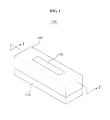
- FIG. 1 is a perspective view illustrating a light emitting device (LED) assembly according to an embodiment of the present invention.
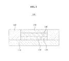
- FIG. 2 is a cross-sectional view cut along the line I-I' of FIG. 1 .
- the LED assembly 100 may include a substrate 110, at least one LED chip 120 mounted on the substrate 110, a first reflection layer 130 formed on a side surface of the at least one LED chip 120, an optical layer 140 formed on the at least one LED chip 120, a phosphor layer 150 formed on the optical layer 140, and a second reflection layer 160 formed on side surfaces of the optical layer 140 and the phosphor layer 150.
- the substrate 110 may be manufactured using a metal, silicon, or ceramic.
- the substrate 110 may correspond to an insulating substrate manufactured using glass or sapphire, and correspond to a conductive substrate manufactured using silicon (Si), silicon carbide (SiC), or zinc oxide (ZnO). That is, the substrate 110 may be manufactured using a material having an excellent heat radiation characteristic.
- An electrode (not shown) may be formed on the substrate 110, and the electrode may include an electric circuit. Here, power may be supplied to the at least one LED chip 120 through the electric circuit.
- the at least one LED chip 120 used as a light source may be mounted on the substrate 110.
- the at least one LED chip 120 is briefly described in the following.
- the at least one LED chip 120 may include a first conductive semiconductor layer, an active layer, a second conductive semiconductor layer, and an electrode.
- the first conductive semiconductor layer may be n-doped. That is, an electron may be moved to the active layer through the first conductive semiconductor layer.
- the active layer may be formed on the first conductive semiconductor layer.
- the active layer may be formed in a laminated structure in which a quantum barrier layer and a quantum well layer are alternately formed so that an electron and a hole may recombine and emit light.
- composition of the active layer may vary depending on a desired emission wavelength.
- the second conductive semiconductor layer may be formed on the active layer.
- the second conductive semiconductor layer may be p-doped. That is, a hole may be moved to the active layer through the second conductive semiconductor layer.
- a transparent electrode may be formed on the second conductive semiconductor layer.
- the transparent electrode may be formed on a transparent metal layer such as nickel (Ni) / gold (Au) or be formed to include a conductive oxide such as indium tin oxide (ITO).
- a p-type electrode may be formed on the transparent electrode, and an n-type electrode may be formed on the first conductive semiconductor layer.
- the p-type electrode and the n-type electrode may include various conductive materials such as titanium (Ti) / aluminum (Al), and the like.
- a hole may be provided through the p-type electrode, and an electron may be provided through the n-type electrode.
- the provided hole and the electron may combine in the active layer to generate light energy.
- the at least one LED chip 120 may correspond to an ultraviolet LED or a blue light LED depending on a desired wavelength of an emitted light.
- the first reflection layer 130 may be formed on a side surface of the at least one LED chip 120.
- the first reflection layer 130 may be formed between the at least one LED chip 120.
- the first reflection layer 130 may be formed to improve dark regions generated in a space between LED chips when there exists a plurality of LED chips 120.
- the first reflection layer 130 may fill in the space between the at least one LED chip 120, thereby improving dark regions where luminance deteriorates in comparison to each portion of the at least one LED chip 120.
- the first reflection layer 130 may reflect light emitted from a side of the at least one LED chip 120 to be delivered to the optical layer 140.
- the optical layer 140 may be formed on the at least one LED chip 120.
- the optical layer 140 may be formed on the first reflection layer 130 that is formed between the LED chips when there exists a plurality of LED chips 120.
- the optical layer 140 may be formed on the entire surface of the plurality of the LED chips 120 rather than being formed on each of the plurality of the LED chips 120 respectively.
- light generated on the at least one LED chip 120 and light generated at a side of the at least one LED chip 120 and delivered by the first reflection layer 130 may be delivered to the phosphor layer 150 through the optical layer 140.
- the optical layer 140 may function as a light guide panel that delivers light generated from the at least one LED chip 120 to the phosphor layer 150.
- the optical layer 140 formed using a transparent material may be disposed between the at least one LED chip 120 and the phosphor layer 150 to prevent direct contact between the at least one LED chip 120 and the phosphor layer 150, thereby reducing a loss of light.
- the optical layer 140 may be formed using a transparent material.
- the optical layer 140 may be formed using silicon.
- the optical layer 140 may be formed using a silicon resin having light transmissivity of at least 90%.
- the optical layer 140 may be formed using at least one material selected from a group consisting of transparent silicon resin composition, epoxy resin, a modified epoxy resin composition, and may not be limited thereto.
- the optical layer 140 may be formed using a transparent material such as glass or an insulating composition of a plastic synthetic resin.
- the optical layer 140 may include a scattering particle, and the scattering particle may correspond to silicon dioxide (SiO 2 ).
- SiO 2 silicon dioxide
- the scattering particle When the scattering particle is included in the optical layer 140, light delivered from the at least one LED chip 120 may be scattered, thereby enhancing light extraction efficiency.
- An upper surface of the optical layer 140 may be patterned. When the upper surface of the optical layer 140 is patterned to have micro-irregularities, an amount of light lost in the optical layer 140 may be reduced, thereby enhancing light extraction efficiency.
- the phosphor layer 150 may be formed on the optical layer 140.
- light emitted from the at least one LED chip 120 may be delivered through the optical layer 140 and emitted to an external environment through the phosphor layer 150.
- the phosphor layer 150 may scatter and color-convert colors of light emitted from the at least one LED chip 120. For example, blue light emitted from the at least one LED chip 120 may be converted to yellow light, green light, or red light through the phosphor layer 150, and white light may be emitted to an external environment.
- the phosphor layer 150 may include a phosphor material that may convert blue light to yellow light, green light, or red light.
- the phosphor layer 150 may include a host material and an active material, and include, for example, a material activated by cerium (Ce) in an yttrium aluminum garnet (YAG) host material.
- YAG yttrium aluminum garnet
- a material activated by europium (Eu) included in a silicate-based host material may be used for the phosphor layer 150, and not be limited thereto.
- the phosphor layer 150 may be formed to have a thin and uniform thickness. That is, phosphor particles may be uniformly distributed in the phosphor layer 150. Thus, colors of light penetrating the phosphor layer 150 may be uniformly color-converted.
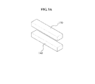
- FIGS. 3A and 3B are diagrams illustrating an optical layer 140 and a phosphor layer 150 in a film form in an LED assembly according to another embodiment of the present invention.
- FIG. 3A illustrates that the optical layer 140 and the phosphor layer 150 are separately manufactured in film forms
- FIG. 3B illustrates that the optical layer 140 and the phosphor layer 150 are manufactured in a film form as one body.
- the optical layer 140 and the phosphor layer 150 may be formed in a film form to be stacked on the at least one LED chip 120 of FIG 2 .
- the optical layer 140 and the phosphor layer 150 may be manufactured separately in film forms to be subsequently stacked on the at least one LED chip 120.
- the optical layer 140 and the phosphor layer 150 may be manufactured in a film form as one body to be stacked on the at least one LED chip 120 in a single operation.
- a manufacturing process may be simplified by initially manufacturing the optical layer 140 and the phosphor layer 150 in a film form.
- the optical layer 140 and the phosphor layer 150 may be formed by applying a liquid material onto the at least one LED chip 120 and a first reflection layer 130 of FIG. 2 and using thermal curing or ultraviolet (UV) curing.
- a liquid material onto the at least one LED chip 120 and a first reflection layer 130 of FIG. 2 and using thermal curing or ultraviolet (UV) curing.
- UV ultraviolet
- the second reflection layer 160 may be formed on side surfaces of the optical layer 140 and the phosphor layer 150 to improve a total luminous flux and obtain contrast in a boundary of a light source portion. That is, when the first reflection layer 130 is formed only between LED chips when there exists a plurality of the at least one LED chip 120, the second reflection layer 160 may be formed on a side surface of the at least one LED chip 120 at an outermost position. The first reflection layer 130 or the second reflection layer 160 may be formed on a side surface of the at least one LED chip 120 at an outermost position.
- High contrast of a light source may be obtained by forming a reflection layer on side surfaces of the at least one LED chip 120, the optical layer 140, and the phosphor layer 150.
- the first reflection layer 130 and the second reflection layer 160 may be formed using the same material.
- the first reflection layer 130 and the second reflection layer 160 may be formed using an oxide that includes one of titanium (Ti), zirconium (Zr), niobium (Nb), aluminum (Al), and silicon (Si) corresponding to a light reflective material, or be formed using a material selected from aluminum nitride (AlN) and magnesium fluoride (MgF 2 ).
- the first reflection layer 130 and the second reflection layer 160 may be formed using a material selected from a group consisting of titanium dioxide (TiO 2 ), zirconium dioxide (ZrO 2 ), niobium pentoxide (Nb 2 O 5 ), aluminum oxide (Al 2 O 3 ), magnesium fluoride (MgF 2 ), aluminum nitride (AlN), and SiO 2 .
- contrast may be enhanced by employing the second reflection layer 160 to prevent light from being emitted to an external environment through a portion other than the phosphor layer 150. Since a separate shield structure for enhancing contrast may be omitted, a loss of light may be minimized and light extraction efficiency may be improved.
- the configurations may be different from the aforementioned LED assembly, for ease of description, descriptions of structures that are similar to, or the same as the structures described in the foregoing with reference to FIG. 1 and Fig. 2 will be omitted, for conciseness, or will be provided as needed.
- FIG. 4 is a perspective view illustrating an LED assembly 200 according to still another embodiment of the present invention.
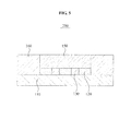
- FIG. 5 is a cross-sectional view cut along the line II-II' of FIG. 4 .
- the LED assembly 200 may include a substrate 110, at least one LED chip 120 mounted on the substrate 110, a first reflection layer 130 formed on a side surface of the at least one LED chip 120, a phosphor layer 150 formed on the at least one LED chip 102 and including a scattering particle, and a second reflection layer 160 formed on a side surface of the phosphor layer 150.
- the phosphor layer 150 may be directly formed on the at least one LED chip 102 and include the scattering particle.
- the scattering particle may be included in the phosphor layer 150 and thus, a low light extraction efficiency may be prevented.
- the scattering particle included in the phosphor layer 150 may correspond to SiO 2 .
- the scattering particle may be included in the phosphor layer 150, light delivered from the at least one LED chip 102 may be scattered, thereby enhancing light extraction efficiency.
- an upper surface of the phosphor layer 150 may be patterned. In this instance, when the upper surface of the optical layer 150 is patterned to have micro-irregularities, an amount of light amount lost in the LED assembly 200 may be reduced, thereby enhancing light extraction efficiency.
- the first reflection layer 130 and the second reflection layer 160 may be formed using an oxide, corresponding to a light reflective material, that includes one of Ti, Zr, Nb, Al, Si or be formed using a material selected from AlN and MgF 2 .
- the first reflection layer 130 and the second reflection layer 160 may be formed using a material selected from a group consisting of TiO 2 , ZrO 2 , Nb 2 O 5 , Al 2 O 3 , MgF 2 , AlN, and SiO 2 .
- the phosphor layer 150 including the scattering particle may be manufactured in a film form to be stacked on the at least one LED chip 120.
- a manufacturing process may be simplified by initially manufacturing the phosphor layer 150 in a film form, and then stacking the phosphor layer 150 on the at least one LED chip 120.
- FIG. 6 is a cross-sectional view roughly illustrating a headlamp for a vehicle according to yet another embodiment of the present invention.
- a headlamp having an LED assembly may include the LED assembly 100 described above, a reflector 310, and a lens 320.
- the reflector 310 may be incorporated in the headlamp to reflect a light generated by the LED assembly 100 at the front of the vehicle, and be formed in a predetermined shape to reflect the light to an area in front of the vehicle.
- the reflector 310 may be provided in various structures, forms and shapes such as a parabolic shape, a straight line type, and an optical reflector structure.
- the lens 320 may project a light reflected by the reflector 310 and emitted to an area in front of the vehicle of the vehicle.
- the lens 320 may correspond to an aspheric lens, and may not be limited thereto.
- an LED assembly may improve dark regions generated between at least one LED chip, may reduce loss of light, and may obtain a relatively high contrast.
- An LED assembly according to an embodiment of the present invention may omit a shield structure and thus, a headlamp for a vehicle may be manufactured in a relatively simple structure.
- An LED assembly may improve dark regions generated between LED chips when there is a plurality of the at least one LED chip 120, by employing a first reflection layer between the LED chips.
- a transparent optical layer or an optical layer including a scattering particle between an LED chip and a phosphor layer direct contact between the LED chip and the phosphor layer may be avoided, thereby preventing a low light extraction efficiency.
- a second reflection layer on side surfaces of an LED chip, an optical layer, and a phosphor layer a relatively high contrast may be obtained.
- An LED assembly according to an aspect of an embodiment of the present invention may enhance contrast through a reflective layer while increasing light extraction efficiency by including a scattering particle in a phosphor layer.
- an LED assembly may improve dark regions generated between LED chips when there exists a plurality of the at least one LED chip 120, reduce a loss of light, and obtain a relatively high contrast.
Landscapes
- Engineering & Computer Science (AREA)
- General Engineering & Computer Science (AREA)
- Physics & Mathematics (AREA)
- Optics & Photonics (AREA)
- Geometry (AREA)
- Microelectronics & Electronic Packaging (AREA)
- Electromagnetism (AREA)
- Non-Portable Lighting Devices Or Systems Thereof (AREA)
- Led Device Packages (AREA)
Applications Claiming Priority (1)
| Application Number | Priority Date | Filing Date | Title |
|---|---|---|---|
| KR1020110046845A KR101798884B1 (ko) | 2011-05-18 | 2011-05-18 | 발광소자 어셈블리 및 이를 포함하는 전조등 |
Publications (2)
| Publication Number | Publication Date |
|---|---|
| EP2525418A2 true EP2525418A2 (de) | 2012-11-21 |
| EP2525418A3 EP2525418A3 (de) | 2016-05-18 |
Family
ID=46125194
Family Applications (1)
| Application Number | Title | Priority Date | Filing Date |
|---|---|---|---|
| EP12167043.4A Withdrawn EP2525418A3 (de) | 2011-05-18 | 2012-05-08 | Gehäuse für lichtemittierende Vorrichtung und Beleuchtungssystem damit |
Country Status (4)
| Country | Link |
|---|---|
| US (3) | US8882319B2 (de) |
| EP (1) | EP2525418A3 (de) |
| KR (1) | KR101798884B1 (de) |
| TW (1) | TWI558944B (de) |
Families Citing this family (12)
| Publication number | Priority date | Publication date | Assignee | Title |
|---|---|---|---|---|
| EP2959215A4 (de) * | 2013-02-25 | 2017-02-01 | Rensselaer Polytechnic Institute | Beleuchtung mit geringer luminanz |
| KR20140115841A (ko) | 2013-03-22 | 2014-10-01 | 삼성디스플레이 주식회사 | 조명장치 및 조명유닛 |
| DE102013205836A1 (de) * | 2013-04-03 | 2014-10-09 | Osram Opto Semiconductors Gmbh | Fahrzeugleuchte |
| JP6307703B2 (ja) * | 2013-05-31 | 2018-04-11 | パナソニックIpマネジメント株式会社 | 波長変換素子、波長変換素子を備えた発光装置、発光装置を備えた車両、および波長変換素子の製造方法 |
| KR102089571B1 (ko) | 2013-07-25 | 2020-03-16 | 현대모비스 주식회사 | 차량용 램프 |
| KR102075993B1 (ko) * | 2013-12-23 | 2020-02-11 | 삼성전자주식회사 | 백색 led 소자들을 제조하는 방법 |
| CN105431953B (zh) * | 2014-06-05 | 2018-03-16 | 上海富迪照明电器有限公司 | 基于固态荧光材料的嵌入式白光led封装结构及其制作方法 |
| DE102015219799A1 (de) * | 2015-10-13 | 2017-04-27 | Osram Gmbh | Konversionsvorrichtung und Fahrzeugscheinwerfer |
| JP6332294B2 (ja) * | 2015-11-30 | 2018-05-30 | 日亜化学工業株式会社 | 発光装置 |
| US10797209B2 (en) * | 2016-02-05 | 2020-10-06 | Maven Optronics Co., Ltd. | Light emitting device with beam shaping structure and manufacturing method of the same |
| US20200263846A1 (en) * | 2019-02-20 | 2020-08-20 | Magna Closures Inc. | Vehicle light assembly with quantum doped material illuminable using distinct illumination sources |
| EP4012507B1 (de) * | 2020-12-11 | 2026-04-01 | The Swatch Group Research and Development Ltd | Phosphoreszierende uhrenkomponente |
Citations (5)
| Publication number | Priority date | Publication date | Assignee | Title |
|---|---|---|---|---|
| US20060083281A1 (en) * | 2004-10-18 | 2006-04-20 | Sharp Kabushiki Kaisha | Semiconductor light emitting device, backlight device for liquid crystal display |
| EP1667228A2 (de) * | 2004-12-02 | 2006-06-07 | Samsung Electro-Mechanics Co., Ltd | Lichtemittierende Halbleitervorrichtung und Herstellungsverfahren |
| TWM309750U (en) * | 2006-10-18 | 2007-04-11 | Lighthouse Technology Co Ltd | Light emitting diode package |
| US20090184333A1 (en) * | 2008-01-17 | 2009-07-23 | Foxsemicon Integrated Technology, Inc. | Light emitting diode device |
| JP2010219324A (ja) * | 2009-03-17 | 2010-09-30 | Nichia Corp | 発光装置 |
Family Cites Families (43)
| Publication number | Priority date | Publication date | Assignee | Title |
|---|---|---|---|---|
| KR100481994B1 (ko) | 1996-08-27 | 2005-12-01 | 세이코 엡슨 가부시키가이샤 | 박리방법,박막디바이스의전사방법,및그것을이용하여제조되는박막디바이스,박막집적회로장치및액정표시장치 |
| USRE38466E1 (en) | 1996-11-12 | 2004-03-16 | Seiko Epson Corporation | Manufacturing method of active matrix substrate, active matrix substrate and liquid crystal display device |
| US7208725B2 (en) | 1998-11-25 | 2007-04-24 | Rohm And Haas Electronic Materials Llc | Optoelectronic component with encapsulant |
| JP3906654B2 (ja) | 2000-07-18 | 2007-04-18 | ソニー株式会社 | 半導体発光素子及び半導体発光装置 |
| EP1179858B1 (de) * | 2000-08-09 | 2009-03-18 | Avago Technologies General IP (Singapore) Pte. Ltd | Lichtemittierende Vorrichtungen |
| WO2003019678A1 (en) | 2001-08-22 | 2003-03-06 | Sony Corporation | Nitride semiconductor element and production method for nitride semiconductor element |
| JP2003218034A (ja) | 2002-01-17 | 2003-07-31 | Sony Corp | 選択成長方法、半導体発光素子及びその製造方法 |
| JP3815335B2 (ja) | 2002-01-18 | 2006-08-30 | ソニー株式会社 | 半導体発光素子及びその製造方法 |
| JP4172196B2 (ja) * | 2002-04-05 | 2008-10-29 | 豊田合成株式会社 | 発光ダイオード |
| KR100499129B1 (ko) | 2002-09-02 | 2005-07-04 | 삼성전기주식회사 | 발광 다이오드 및 그 제조방법 |
| US7002182B2 (en) | 2002-09-06 | 2006-02-21 | Sony Corporation | Semiconductor light emitting device integral type semiconductor light emitting unit image display unit and illuminating unit |
| JP2004127662A (ja) * | 2002-10-01 | 2004-04-22 | Sony Corp | 表示装置 |
| US6917057B2 (en) | 2002-12-31 | 2005-07-12 | Gelcore Llc | Layered phosphor coatings for LED devices |
| KR100714639B1 (ko) | 2003-10-21 | 2007-05-07 | 삼성전기주식회사 | 발광 소자 |
| KR100506740B1 (ko) | 2003-12-23 | 2005-08-08 | 삼성전기주식회사 | 질화물 반도체 발광소자 및 그 제조방법 |
| US7517728B2 (en) * | 2004-03-31 | 2009-04-14 | Cree, Inc. | Semiconductor light emitting devices including a luminescent conversion element |
| CN100411207C (zh) * | 2004-06-28 | 2008-08-13 | 京瓷株式会社 | 发光装置及照明装置 |
| KR100664985B1 (ko) | 2004-10-26 | 2007-01-09 | 삼성전기주식회사 | 질화물계 반도체 소자 |
| TWI237411B (en) * | 2004-12-06 | 2005-08-01 | Internat Semiconductor Technol | Process and structure for packaging LED's |
| KR100665219B1 (ko) | 2005-07-14 | 2007-01-09 | 삼성전기주식회사 | 파장변환형 발광다이오드 패키지 |
| KR100665222B1 (ko) | 2005-07-26 | 2007-01-09 | 삼성전기주식회사 | 확산재료를 이용한 엘이디 패키지 및 그 제조 방법 |
| WO2007018039A1 (ja) * | 2005-08-05 | 2007-02-15 | Matsushita Electric Industrial Co., Ltd. | 半導体発光装置 |
| JP4579094B2 (ja) | 2005-08-23 | 2010-11-10 | 株式会社小糸製作所 | 車両用前照灯 |
| KR100661614B1 (ko) | 2005-10-07 | 2006-12-26 | 삼성전기주식회사 | 질화물계 반도체 발광소자 및 그 제조방법 |
| KR100723247B1 (ko) | 2006-01-10 | 2007-05-29 | 삼성전기주식회사 | 칩코팅형 led 패키지 및 그 제조방법 |
| KR100735325B1 (ko) | 2006-04-17 | 2007-07-04 | 삼성전기주식회사 | 발광다이오드 패키지 및 그 제조방법 |
| KR100930171B1 (ko) | 2006-12-05 | 2009-12-07 | 삼성전기주식회사 | 백색 발광장치 및 이를 이용한 백색 광원 모듈 |
| KR100855065B1 (ko) | 2007-04-24 | 2008-08-29 | 삼성전기주식회사 | 발광 다이오드 패키지 |
| KR100982980B1 (ko) | 2007-05-15 | 2010-09-17 | 삼성엘이디 주식회사 | 면 광원 장치 및 이를 구비하는 lcd 백라이트 유닛 |
| KR101164026B1 (ko) | 2007-07-12 | 2012-07-18 | 삼성전자주식회사 | 질화물계 반도체 발광소자 및 그 제조방법 |
| TWM334470U (en) * | 2007-08-14 | 2008-06-11 | Wellypower Optronics Corp | Light emitting diode device |
| KR100891761B1 (ko) | 2007-10-19 | 2009-04-07 | 삼성전기주식회사 | 반도체 발광소자, 그의 제조방법 및 이를 이용한 반도체발광소자 패키지 |
| KR101332794B1 (ko) | 2008-08-05 | 2013-11-25 | 삼성전자주식회사 | 발광 장치, 이를 포함하는 발광 시스템, 상기 발광 장치 및발광 시스템의 제조 방법 |
| KR20100030470A (ko) | 2008-09-10 | 2010-03-18 | 삼성전자주식회사 | 다양한 색 온도의 백색광을 제공할 수 있는 발광 장치 및 발광 시스템 |
| KR101530876B1 (ko) | 2008-09-16 | 2015-06-23 | 삼성전자 주식회사 | 발광량이 증가된 발광 소자, 이를 포함하는 발광 장치, 상기 발광 소자 및 발광 장치의 제조 방법 |
| US8008683B2 (en) | 2008-10-22 | 2011-08-30 | Samsung Led Co., Ltd. | Semiconductor light emitting device |
| KR101639788B1 (ko) * | 2009-03-19 | 2016-07-15 | 코닌클리케 필립스 엔.브이. | 컬러 조절 장치 |
| JP5482378B2 (ja) * | 2009-04-20 | 2014-05-07 | 日亜化学工業株式会社 | 発光装置 |
| JP5326837B2 (ja) * | 2009-06-08 | 2013-10-30 | 日亜化学工業株式会社 | 発光装置 |
| US20110062469A1 (en) | 2009-09-17 | 2011-03-17 | Koninklijke Philips Electronics N.V. | Molded lens incorporating a window element |
| KR101094251B1 (ko) * | 2009-09-30 | 2011-12-19 | 허재원 | 전방위로 조사되는 led 모듈 |
| JP4919179B2 (ja) * | 2010-05-11 | 2012-04-18 | 独立行政法人電子航法研究所 | ミリ波レーダ組み込み型ヘッドランプ |
| TWM397595U (en) * | 2010-08-05 | 2011-02-01 | Unity Opto Technology Co Ltd | LED structure |
-
2011
- 2011-05-18 KR KR1020110046845A patent/KR101798884B1/ko active Active
-
2012
- 2012-05-08 EP EP12167043.4A patent/EP2525418A3/de not_active Withdrawn
- 2012-05-11 TW TW101116805A patent/TWI558944B/zh active
- 2012-05-18 US US13/475,486 patent/US8882319B2/en active Active
-
2014
- 2014-01-09 US US14/151,733 patent/US8921883B2/en active Active
- 2014-12-18 US US14/575,741 patent/US9188300B2/en active Active
Patent Citations (5)
| Publication number | Priority date | Publication date | Assignee | Title |
|---|---|---|---|---|
| US20060083281A1 (en) * | 2004-10-18 | 2006-04-20 | Sharp Kabushiki Kaisha | Semiconductor light emitting device, backlight device for liquid crystal display |
| EP1667228A2 (de) * | 2004-12-02 | 2006-06-07 | Samsung Electro-Mechanics Co., Ltd | Lichtemittierende Halbleitervorrichtung und Herstellungsverfahren |
| TWM309750U (en) * | 2006-10-18 | 2007-04-11 | Lighthouse Technology Co Ltd | Light emitting diode package |
| US20090184333A1 (en) * | 2008-01-17 | 2009-07-23 | Foxsemicon Integrated Technology, Inc. | Light emitting diode device |
| JP2010219324A (ja) * | 2009-03-17 | 2010-09-30 | Nichia Corp | 発光装置 |
Also Published As
| Publication number | Publication date |
|---|---|
| TWI558944B (zh) | 2016-11-21 |
| US8882319B2 (en) | 2014-11-11 |
| US20150103547A1 (en) | 2015-04-16 |
| US20120294025A1 (en) | 2012-11-22 |
| EP2525418A3 (de) | 2016-05-18 |
| US20140124815A1 (en) | 2014-05-08 |
| KR101798884B1 (ko) | 2017-11-17 |
| KR20120128909A (ko) | 2012-11-28 |
| US9188300B2 (en) | 2015-11-17 |
| US8921883B2 (en) | 2014-12-30 |
| TW201250152A (en) | 2012-12-16 |
Similar Documents
| Publication | Publication Date | Title |
|---|---|---|
| US9188300B2 (en) | Light emitting device assembly and headlamp including the same | |
| US9496465B2 (en) | Light emitting device | |
| US9508908B2 (en) | LED with scattering features in substrate | |
| JP5059208B2 (ja) | 照明装置および車両用前照灯 | |
| KR102024291B1 (ko) | 램프 유닛 및 그를 이용한 차량 램프 장치 | |
| US8807812B2 (en) | Light emitting device, illuminating device, and headlamp | |
| US20110248623A1 (en) | Light emitting device | |
| KR20190132124A (ko) | 조명 모듈 및 이를 구비한 조명 장치 | |
| JP2012099282A (ja) | 照明装置及び車両用前照灯 | |
| JP2009070892A (ja) | Led光源 | |
| KR20200134466A (ko) | 발광소자패키지 및 광원장치 | |
| JP2010219163A (ja) | 発光モジュール、および灯具ユニット | |
| EP3480517B1 (de) | Phosphormodul | |
| JP5678462B2 (ja) | 発光装置 | |
| US11067242B2 (en) | Phosphor module | |
| JPWO2010103840A1 (ja) | 発光モジュール、および灯具ユニット | |
| CN221783239U (zh) | 半导体发光器件 | |
| KR20190010988A (ko) | 자동차 헤드램프용 발광 다이오드 | |
| CN110869665B (zh) | 照明模块 | |
| KR20200134756A (ko) | 발광소자패키지 및 광원장치 | |
| KR102426861B1 (ko) | 발광 소자 패키지 | |
| JP7518374B2 (ja) | 発光装置 | |
| CN209638932U (zh) | 发光模块 | |
| CN117558858A (zh) | 半导体发光器件 | |
| KR20120051938A (ko) | 발광소자 어셈블리 |
Legal Events
| Date | Code | Title | Description |
|---|---|---|---|
| PUAI | Public reference made under article 153(3) epc to a published international application that has entered the european phase |
Free format text: ORIGINAL CODE: 0009012 |
|
| 17P | Request for examination filed |
Effective date: 20120508 |
|
| AK | Designated contracting states |
Kind code of ref document: A2 Designated state(s): AL AT BE BG CH CY CZ DE DK EE ES FI FR GB GR HR HU IE IS IT LI LT LU LV MC MK MT NL NO PL PT RO RS SE SI SK SM TR |
|
| AX | Request for extension of the european patent |
Extension state: BA ME |
|
| RIC1 | Information provided on ipc code assigned before grant |
Ipc: H01L 33/46 20100101AFI20151117BHEP Ipc: H01L 33/50 20100101ALI20151117BHEP Ipc: F21S 8/12 20060101ALI20151117BHEP Ipc: F21S 8/10 20060101ALN20151117BHEP |
|
| PUAL | Search report despatched |
Free format text: ORIGINAL CODE: 0009013 |
|
| AK | Designated contracting states |
Kind code of ref document: A3 Designated state(s): AL AT BE BG CH CY CZ DE DK EE ES FI FR GB GR HR HU IE IS IT LI LT LU LV MC MK MT NL NO PL PT RO RS SE SI SK SM TR |
|
| AX | Request for extension of the european patent |
Extension state: BA ME |
|
| RIC1 | Information provided on ipc code assigned before grant |
Ipc: F21S 8/12 20060101ALI20160413BHEP Ipc: H01L 33/50 20100101ALI20160413BHEP Ipc: F21S 8/10 20060101ALN20160413BHEP Ipc: H01L 33/46 20100101AFI20160413BHEP |
|
| RBV | Designated contracting states (corrected) |
Designated state(s): AL AT BE BG CH CY CZ DE DK EE ES FI FR GB GR HR HU IE IS IT LI LT LU LV MC MK MT NL NO PL PT RO RS SE SI SK SM TR |
|
| 17Q | First examination report despatched |
Effective date: 20180425 |
|
| STAA | Information on the status of an ep patent application or granted ep patent |
Free format text: STATUS: THE APPLICATION IS DEEMED TO BE WITHDRAWN |
|
| 18D | Application deemed to be withdrawn |
Effective date: 20201009 |