EP2529262B1 - Interconnexions de fibres optiques à un guide d'ondes basées sur un réseau - Google Patents
Interconnexions de fibres optiques à un guide d'ondes basées sur un réseau Download PDFInfo
- Publication number
- EP2529262B1 EP2529262B1 EP10844895.2A EP10844895A EP2529262B1 EP 2529262 B1 EP2529262 B1 EP 2529262B1 EP 10844895 A EP10844895 A EP 10844895A EP 2529262 B1 EP2529262 B1 EP 2529262B1
- Authority
- EP
- European Patent Office
- Prior art keywords
- grating
- waveguide
- optical fiber
- interconnect
- light
- Prior art date
- Legal status (The legal status is an assumption and is not a legal conclusion. Google has not performed a legal analysis and makes no representation as to the accuracy of the status listed.)
- Active
Links
Images







Classifications
-
- G—PHYSICS
- G02—OPTICS
- G02B—OPTICAL ELEMENTS, SYSTEMS OR APPARATUS
- G02B6/00—Light guides; Structural details of arrangements comprising light guides and other optical elements, e.g. couplings
- G02B6/24—Coupling light guides
- G02B6/26—Optical coupling means
- G02B6/30—Optical coupling means for use between fibre and thin-film device
-
- G—PHYSICS
- G02—OPTICS
- G02B—OPTICAL ELEMENTS, SYSTEMS OR APPARATUS
- G02B6/00—Light guides; Structural details of arrangements comprising light guides and other optical elements, e.g. couplings
- G02B6/02—Optical fibres with cladding with or without a coating
- G02B6/02057—Optical fibres with cladding with or without a coating comprising gratings
- G02B6/02061—Grating external to the fibre and in contact with the fibre, e.g. evanescently coupled, gratings applied to the fibre end
-
- G—PHYSICS
- G02—OPTICS
- G02B—OPTICAL ELEMENTS, SYSTEMS OR APPARATUS
- G02B6/00—Light guides; Structural details of arrangements comprising light guides and other optical elements, e.g. couplings
- G02B6/10—Light guides; Structural details of arrangements comprising light guides and other optical elements, e.g. couplings of the optical waveguide type
- G02B6/12—Light guides; Structural details of arrangements comprising light guides and other optical elements, e.g. couplings of the optical waveguide type of the integrated circuit kind
- G02B6/122—Basic optical elements, e.g. light-guiding paths
- G02B6/124—Geodesic lenses or integrated gratings
-
- G—PHYSICS
- G02—OPTICS
- G02B—OPTICAL ELEMENTS, SYSTEMS OR APPARATUS
- G02B6/00—Light guides; Structural details of arrangements comprising light guides and other optical elements, e.g. couplings
- G02B6/24—Coupling light guides
- G02B6/26—Optical coupling means
- G02B6/30—Optical coupling means for use between fibre and thin-film device
- G02B6/305—Optical coupling means for use between fibre and thin-film device and having an integrated mode-size expanding section, e.g. tapered waveguide
-
- G—PHYSICS
- G02—OPTICS
- G02B—OPTICAL ELEMENTS, SYSTEMS OR APPARATUS
- G02B6/00—Light guides; Structural details of arrangements comprising light guides and other optical elements, e.g. couplings
- G02B6/24—Coupling light guides
- G02B6/26—Optical coupling means
- G02B6/34—Optical coupling means utilising prism or grating
-
- G—PHYSICS
- G02—OPTICS
- G02B—OPTICAL ELEMENTS, SYSTEMS OR APPARATUS
- G02B6/00—Light guides; Structural details of arrangements comprising light guides and other optical elements, e.g. couplings
- G02B6/10—Light guides; Structural details of arrangements comprising light guides and other optical elements, e.g. couplings of the optical waveguide type
- G02B6/12—Light guides; Structural details of arrangements comprising light guides and other optical elements, e.g. couplings of the optical waveguide type of the integrated circuit kind
- G02B2006/12083—Constructional arrangements
- G02B2006/12107—Grating
Definitions
- Embodiments of the present invention relate to optical fiber-to-waveguide couplers.
- Coupling light between optical fibers and waveguides is an indispensable part of any on- and off-chip optical communication system.
- coupling light from an optical fiber into a waveguide, or coupling light from a waveguide into an optical fiber presents a number of problems.
- conventional techniques for coupling light from a waveguide into an optical fiber include configuring the end of the waveguide to scatter the light carried by the waveguide and positioning a lens at or near the end the optical fiber to direct a portion of the scattered light in the optical fiber core.
- a lens can be used to direct the maximal ray of the focused beam within the numerical aperture of the fiber core, in this way the light captured by the lens can be effective coupled into the fiber core.
- the mode of the fiber core and the mode of the light captured by the lens must be closely matched.
- One conventional technique to couple light between a single mode fiber and a waveguide is to use a grating coupler.
- Light coming from the waveguide propagates through the grating and is scattered in free space at some finite angle from normal.
- the collecting fiber therefore needs to be positioned at an angle from normal for efficient coupling. Normal input/output operation is possible but not very efficient due to the coupling between left and right propagating waves in the grating region.
- positioning the fiber at an angle can be done, it often complicates the design and packaging of the chip.
- US2009/290837 A1 relates to an optical device and an optical system for coupling of light.
- the optical device comprises a planar substrate; and an optical waveguiding layer disposed on the planar substrate.
- the optical waveguiding layer comprises a grating portion for coupling light between a planar waveguide and an optical fiber; and a tapered guiding portion for converting the mode size between the fiber and the planar waveguide.
- the grating portion comprises a first grating section having non-uniform periods.
- SHIN W ET AL "Microstructured Fiber End Surface Grating for Coarse WDM Signal Monitoring", IEEE PHOTONICS TECHNOLOGY LETTERS, IEEE SERVICE CENTER, PISCATAWAY, NJ, US, (20070415), vol. 19, no. 8, ISSN 1041-1135, pages 550 - 552, XP011175013 discloses an optical fiber having an end surface grating for use in Coarse Wave Division Multiplexing signal measurements, diffracted beams from the grating being collimated and fed to an infrared vidicon.
- Embodiments of the present invention are directed to optical waveguide-to-fiber interconnects.
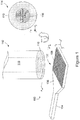
- Figure 1 shows an isometric view of an example optical fiber-to-waveguide interconnect 100 configured in accordance with one or more embodiments of the present invention.
- the interconnect 100 includes a grating coupler 102 formed at the end of a waveguide 104.
- the grating coupler 102 includes a tapered waveguide 106 and a grating block 108.
- the grating block 108 includes a grating composed of a series of lines separated by grooves oriented approximately perpendicular to the waveguide 104.
- the interconnect 100 also includes a grating layer 110 disposed on a planarized end of an optical fiber 112,
- Figure 1 also includes an end-on-view 14 of the grating layer 110, revealing the grating layer includes a planar, non-periodic, sub-wavelength grating ("SWG") 116.
- the SWG 116 is located approximately in the center of the grating layer 110 and is dimensioned to cover the end of the core 118 of the optical fiber 112.
- Figure 1 also reveals the grating coupler 102 and the grating layer 110 are separated by air space and the end portion of the optical fiber 112 is oriented substantially perpendicular to the plane of the grating coupler 102.
- the waveguide 104 has a considerably smaller cross-sectional area than the cross-sectional area of the core 118.
- the optical fiber 112 can be a single mode fiber or a multimode fiber.
- the width of the waveguide can range from approximately 2-4 ⁇ m
- the diameter of the core 118 for a single mode fiber can range from approximately 8-12 ⁇ m
- the diameter of the core 118 for a multimode fiber can range from approximately 20-70 ⁇ m.
- the interconnect 100 can be operated to couple light from the smaller dimensioned waveguide 104 into the relatively larger dimensioned core 118, and the interconnect 100 can be operated in reverse to couple light from the core 118 into the waveguide 104.
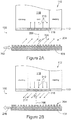
- FIG. 2A shows a cross-sectional view of the interconnect 100, along a line A-A shown in Figure 1 , operated to couple light from the waveguide 104 into the core 118 in accordance with one or more embodiments of the present invention.
- a grating 204 formed within the grating block 108 causes light 202 to exit the grating block 108 with an angle ⁇ to normal 206, as indicated by directional arrows 208.
- the SWG 116 is configured so that light exiting the grating block 108, and incident on the SWG 116 with the angle ⁇ , is transmitted into the core 118, as indicated by directional arrows 210.
- Figure 2B shows a cross-sectional view of the interconnect 100, along the line A-A shown in Figure 1 , operated to couple light from the core 118 into the waveguide 104 in accordance with one or more embodiments of the present invention.
- light transmitted along the core 118 to sub-wavelength grating 116 is represented by directional arrows 212.
- the SWG 116 is configured so that the light transmitted through the SWG 116 is incident on the grating 204 with the angle ⁇ , represented by directional arrows 214.
- the grating 204 captures the light exiting the SWG 116.
- the light 216 exits the grating block 108 and is funneled by the tapered waveguide 106 into the narrower waveguide 104, Note that the SWG 116 is configured to direct the light at the grating block 108 with the angle ⁇ so that the light can be funneled into the waveguide 104.
- the SWG 116 avoids the need to tilt the optical fiber in order to collect light output from the grating block 108.
- the SWG 116 can also operate as an antireflective coating by trapping incident light and projecting the light from the near field into the far field, as described below with reference to Figure 4 .
- the waveguide 104, tapered waveguide 106, and grating block 108 can be formed as a single solid substantial piece of, or integral, semiconductor or dielectric material.
- Semiconductors include, but are not limited to, elemental semiconductors, such as silicon (“Si”) and germanium (“Ge”); and compound semiconductors.
- Compound semiconductors include III-V compound semiconductors and II-VI compound semiconductors.
- III-V compound semiconductors are composed of column IIIa elements selected from boron (“B”), aluminum (“Al”), gallium (“Ga”), and indium (“In”) in combination with column Va elements selected from nitrogen (“N”), phosphorus (“P”), arsenic (“As”), and antimony (“Sb”).
- III-V compound semiconductors are classified according to the relative quantities of III and V elements, such as binary compound semiconductors, ternary compound semiconductors, quaternary compound semiconductors.
- binary semiconductor compounds include, but are not limited to, GaAs, GaAl, InP, InAs, and GaP
- ternary compound semiconductors include, but are not limited to, In y Ga y -1 As or GaAs y P 1- y , where y ranges between 0 and 1
- quaternary compound semiconductors include, but are not limited to, In x Ga 1- x As y P 1- y , where both x and y independently range between 0 and 1.
- II-VI compound semiconductors are composed of column IIb elements selected from zinc (“Zn”), cadmium (“Cd”), mercury (“Hg") in combination wife VIa elements selected from oxygen (“O”), sulfur (“S”), and selenium (“Se”).
- suitable II-VI compound semiconductors includes, but are not limited to, CdSe, ZnSe, ZnS, and ZnO are examples of binary II-VI compound semiconductors.
- Suitable dielectric materials include silicon oxide (“SiO 2 "), aluminum oxide (“Al 2 O 3 "), and silicon carbide (“SiC”).
- the grating coupler 102 can be formed by first depositing the material using chemical vapor deposition, physical vapor deposition, or wafer bonding on a substrate.
- the waveguide 104, tapered waveguide 106, and grating block 108 with grating 204 can then be formed using nanoimprint lithography, photolithography, reactive ion etching, focusing beam milling, or any other suitable well-known method for forming ridge waveguides and gratings.
- FIG 3A shows a top plan view of a SWG 300 configured with a one-dimensional grating pattern formed in a grating layer 301 in accordance with one or more embodiments of the present invention.
- the one-dimensional grating pattern is composed of a number of one-dimensional grating sub-patterns.
- three grating sub-patterns 301-303 are enlarged.
- each grating sub-pattern comprises a number of regularly spaced wire-like portions of the grating layer 102 material called "lines" formed in the grating layer 301.
- the lines extend in the y -direction and are periodically spaced in the x -direction.
- Figure 3A also includes an enlarged end-on view 304 of the grating sub-pattern 302.
- the lines 306 are separated by grooves 308.
- Each sub-pattern can be characterized by a particular periodic spacing of the lines and by the line width in the x -direction.
- the sub-pattern 301 comprises lines of width w 1 separated by a period p 1
- the sub-pattern 302 comprises lines with width w 2 separated by a period p 2
- the sub-pattern 303 comprises lines with width w 3 separated by a period p 3 .
- the line spacing, thickness, and periods can be continuously varying.
- the grating sub-patterns 301-303 form sub-wavelength gratings that preferentially transmit incident light polarized in one direction, i.e., the x -direction, provided the periods p 1 , p 2 , and p 3 are smaller than the wavelength of the incident light.
- the lines widths can range from approximately 10 nm to approximately 300 nm and the periods can range from approximately 20 nm to approximately 1 ⁇ m depending on the wavelength of the incident light.
- the SWG 300 can be configured to apply a particular phase change to transmitted light while maintaining a very high transmissivity.
- the one-dimensional SWG 300 can be configured to transmit light the x -polarized component or the y- polarized component of incident light by adjusting the period, line width and line thickness of the lines. For example, a particular period, line width and line thickness may be suitable for transmitting the x -polarized component but not for transmitted the y- polarized component; and a different period, line width and line thickness may be suitable for transmitting the y- polarized component but not for transmitting the x- polarized component.
- Embodiments of the present invention are not limited to one-dimensional SWGs.
- a SWG can be configured with a two-dimensional, non-periodic grating pattern to transmit polarity insensitive light.
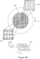
- Figures 3B-3C show top plan views of two example grating layers including two-dimensional SWGs in accordance with one or more embodiments of the present invention.
- the SWG 310 is composed of posts rather lines separated by grooves. The duty cycle and period can be varied in the x - and y -directions.
- Enlargements 312 and 314 show top views of two different rectangular-shaped post sizes.
- Figure 3B includes an isometric view 316 of posts comprising the enlargement 312.
- Embodiments of the present invention are not limited to rectangular-shaped posts, in other embodiments the posts can be square, circular, elliptical, or any other suitable shape.
- the SWG 318 is composed of holes rather than posts.
- Enlargements 320 and 322 show two different rectangular-shaped hole sizes. The duty cycle can be varied in the x - and y- directions.
- Figure 3C includes an isometric view 324 of the enlargement 320.
- the holes shown in Figure 3C are rectangular shaped, in other embodiments, the holes can be square, circular, elliptical or any other suitable shape.
- the one-dimensional and two-dimensiona! grating patterns are described as being composed of sub-patterns, in practice, the period, duty cycle, and thickness of the lines, posts, and holes of the one- and two-dimensional gratings can be continuously varying.
- Figure 4 shows a cross-sectional view of lines from two separate regions of an example SWG revealing the phase acquired by transmitted light in accordance with one or more embodiments of the present invention.
- lines 402 and 403 can be lines in a first region of the SWG
- lines 404 and 405 can be lines in a second region of the same SWG.
- the thickness t 1 of the lines 402 and 403 is greater than the thickness t 2 of the lines 404 and 405, and the duty cycle ⁇ 1 associated with the lines 402 and 403 is also greater than the duty cycle ⁇ 2 associated with the lines 404 and 405.
- the incident waves 408 and 410 strike the lines 402-405 with approximately the same phase, but the wave 412 transmitted through the lines 402 and 403 acquires a relatively larger phase shift ⁇ than the phase ⁇ ' (i.e., ⁇ > ⁇ ') acquired by the wave 414 transmitted through the lines 404 and 405.
- Figure 5 shows a cross-sectional view of the lines 402-405 revealing how the transmitted wavefront changes in accordance with one or more embodiments of the present invention.
- incident light with a substantially uniform wavefront 502 strikes the lines 402-405 producing transmitted light with a curved transmitted wavefront 504.
- the curved wavefront 504 results from portions of the incident wavefront 502 interacting with the lines 402 and 403 with a relatively larger duty cycle ⁇ 1 and thickness t 1 than portions of the same incident wavefront 502 interacting with the lines 404 and 405 with a relatively smaller duty cycle ⁇ 2 and thickness t 2 .
- the shape of the transmitted wavefront 504 is consistent with the larger phase acquired by light striking the lines 402 and 403 relative to the smaller phase acquired by light striking the lines 404 and 405.
- FIG. 6 shows an isometric view of an exemplary phase change contour map 600 produced by a particular SWG 602 of a grating layer 604 in accordance with one or more embodiments of the present invention.
- the contour map 600 represents the magnitude of the phase change acquired by light transmitted through the SWG 602.
- the SWG 602 produces a contour map 602 with the largest magnitude in the phase acquired by the light transmitted near the center of the SWG 602 and with the magnitude of the phase acquired by transmitted light decreasing away from the center of the SWG 602.
- light transmitted through a region 606 acquires a phase of ⁇ 1
- light transmitted through a region 608 acquires a phase of ⁇ 2 . Because ⁇ 1 is much larger than ⁇ 2 , the light transmitted through the regions 606 acquires a much larger phase than the light transmitted through the region 608.
- the phase change in turn shapes the wavefront of light transmitted through a SWG.
- a region having a relatively larger duty cycle produces a larger phase shift in transmitted light than a region having a relatively smaller duty cycle.
- a portion of a wavefront transmitted through a region with a large duty cycle lags behind a second portion of the same wavefront transmitted through a different region with smaller duty cycle.
- Embodiments of the present invention include patterning the SWG to control the phase change and ultimately the shape of the transmitted wavefront so that the SWG can be operated similar to a prism.
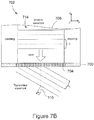
- Figures 7A-7B shows a side view of an example grating layer 700 attached to an end of an optical fiber 702 and operated in accordance with embodiments of the present invention.
- the grating layer 700 includes a SWG 704 configured to transmit light with a wavelength ⁇ .
- light incident on the SWG 704 is represented by incident wavefront 708 and strikes the SWG 704 at an angle of incidence ⁇ to the normal 710.
- the SWG 704 is configured to linearly vary the phase of the incident wavefront 708 to produce transmitted wavefront 712, which propagates along the core 706.
- incident light with the wavelength ⁇ propagating along the core 706 to the SWG 704 is represented by incident wavefront 714.
- the incident light is transmitted through the SWG 104 with a transmitted angle ⁇ to produce transmitted wavefront 716.
- the SWG 704 can be configured to produce a transmitted wavefront with any desired shape, or the SWG 704 can be configured to scatter incident light into the core 706.
- the optical fiber 702 can be a single mode fiber or a multimode fiber.
- the SWG 704 can be configured with dimensions that support coupling the TEM 00 mode into and out of the core 706.
- the SWG 704 can be configured with larger dimensions to support coupling other TEM mn modes into and out of the fiber core 706.
- a SWG can be designed to transmit incident light and introduce a desired phase front by varying the period and duty cycle.
- Figure 8 shows a phase contour plot for transmitted light as a function of period and duty cycle obtained in accordance with one or more embodiments of the present invention using either the well-known finite element method or rigorous coupled wave analysis.
- Contour lines, such as contour lines 801-803 each correspond to a particular phase acquired by light transmitted through region of a SWG with a period and duty cycle lying anywhere along the contour.
- the phase contours are separated by 0.25 ⁇ rad.
- contour 801 corresponds to periods and duty cycles that apply a phase of -0.25 ⁇ rad to transmitted light
- contour 802 corresponds to periods and duty cycles that apply a phase of -0.5 ⁇ rad to transmitted light.
- phase contour can be obtained using either the application "MIT Electromagnetic Equation Propagation” (“MEEP”) simulation package to model electromagnetic systems (ab-initio.mit.edu/meep/meep-1.1.1.tar.gz), or COMSOL Multiphysies® which is a finite element analysis and solver software package that can be used to simulate various physics and engineering applications (see, www.comsol.com).
- MEEP MIT Electromagnetic Equation Propagation
- the points ( p , ⁇ , ⁇ ) represented by the phase contour plot can be used to select periods and duty cycles for a SWG that can be operated as a particular type of lens or prism.
- the data represented in the phase contour plot of Figure 8 can be used to design SWG with particular optical properties.
- the period or duty cycle can be fixed while the other parameter is varied to design and fabricate SWGs. In other embodiments, both the period and duty cycle can be varied to design and fabricate SWGs.
- FIG. 9A shows a top plan view of a grating layer 900 configured with a one-dimensional SWG 902 to operate in accordance with one or more embodiments of the present invention.
- Each shaded region of the SWG 902 represents a different grating sub-pattern of lines extending in the y -direction, with darker shaded regions, such as region 904, representing regions with a relatively larger duty cycle than lighter shaded regions, such as region 906.
- Figure 9A includes enlargements 908 and 910 of two subregions revealing that the lines run parallel in the y -direction. Enlargements 908 and 910 also reveal that the line width w , or duty cycle ⁇ , decreases the x -direction.
- the SWG 902 represents a configuration in which light of an appropriate wavelength and polarized in the x -direction is transmitted through the SWG with a linearly varying wavefront, as described above with reference to Figures 7A and 7B .
- the SWG can be configured so transmit light polarized in any direction by appropriately tapering the lines of the SWG.
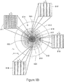
- Figure 9B shows a top plan view of a grating layer 912 configured to operate in accordance with one or more embodiments of the present invention.
- the grating layer 912 includes a SWG 914 with a grating pattern represented by annular shaded regions 916-920. Each annular region represents a different grating sub-pattern of lines.
- Enlargements 916-919 show that the SWG 914 comprises lines tapered in the y -direction with a constant line period spacing p in the x -direction.
- Enlargements 916-919 are enlargements of the same lines running parallel to dashed-line 920 in the y -direction. Enlargements 916-919 reveal that the line period spacing p remains constant but the width of the lines narrow or taper away from the center of the SWG 914 in the y -direction.
- Each annular region has the same duty cycle and period. For example, enlargements 916, 918, and 919 have substantially the same duty cycle. As a result, each portion of an annular region produces the same approximate phase shift in the light transmitted through the SWG 914.
- dashed circle 922 represents a single phase shift contour in which light transmitted through the SWG anywhere along the circle 922 acquires substantially the same phase ⁇ .
- the grating layer can also be configured with a two-dimensional SWG in order to couple unpolarized incident light into or out of an optical fiber core.
- Figures 10A-10B show a top plan views of two two-dimensional SWGs in accordance with one or more embodiments of the present invention.
- a SWG 1002 is composed of posts as described above with reference to Figure 3B .
- the duty cycle and period can be varied in the x - and y -directions.
- Enlargements 1004 and 1006 show the size of the posts decreasing in the x -direction.
- a SWG 1008 is composed of holes as described above with reference to Figure 3C .
- the duty cycle and period can also be varied in the x- and y -directions.
- Enlargements 1010 and 1012 show the size of the holes increasing in the x-direction.
- the SWGs 1002 and 1008 are a configuration so that light of an appropriate is transmitted through the SWGs with a linearly varying wavefront, as described above with reference to Figures 7A and 7B
- a SWG can be fabricated in a grating layer composed of a high refractive index material.
- the grating layer can be composed of, but is not limited to, an elemental semiconductor, a III-V semiconductor, a II-VI semiconductor, or a dielectric material.
- the grating layer can be deposited directly on the end of a planarized optical fiber using wafer bonding, chemical vapor deposition, or physical vapor deposition.
- the SWG can be formed in the grating layer using reactive ion etching, focused ion beam milling, nanoimprint lithography, or photolithography.
- the SWG can be formed using any suitable well-known technique.
Landscapes
- Physics & Mathematics (AREA)
- General Physics & Mathematics (AREA)
- Optics & Photonics (AREA)
- Engineering & Computer Science (AREA)
- Microelectronics & Electronic Packaging (AREA)
- Diffracting Gratings Or Hologram Optical Elements (AREA)
- Optical Couplings Of Light Guides (AREA)
- Optical Integrated Circuits (AREA)
Claims (11)
- Interconnexion de fibres optiques en un guide d'ondes, comprenant :un guide d'ondes ;une fibre optique (112) ;un coupleur de réseau (102) situé à l'extrémité du guide d'ondes ; etune couche de réseau (110) disposée sur l'extrémité de la fibre optique (112), la fibre optique (112) comprenant un noyau (118) et la couche de réseau (110) comprenant un réseau de sous-longueurs d'onde plan et non périodique, (116), la lumière portée par le guide d'ondes dans le coupleur de réseau (102) pouvant être sortie et couplée au noyau (118) par l'intermédiaire du réseau de sous-longueurs d'onde (116), et la lumière transmise le long du noyau à la couche de réseau (110) pouvant être dirigée par le réseau de sous-longueurs d'onde (116) dans le coupleur du réseau pour transmission dans le guide d'ondes.
- Interconnexion selon la revendication 1, dans laquelle le coupleur de réseau comprend en outre un guide d'ondes conique (106) fixé au guide d'ondes, et un bloc de réseau fixé au guide d'ondes conique.
- Interconnexion selon la revendication 2, dans laquelle le coupleur de réseau comprend en outre le guide d'ondes, le guide d'ondes conique et le bloc de réseau composé d'un matériau d'un seul tenant.
- Interconnexion selon la revendication 1, dans laquelle le réseau de sous-longueurs d'onde comprend en outre un motif de réseau unidimensionnel (300).
- Interconnexion selon la revendication 1, dans laquelle le réseau de sous-longueurs d'onde comprend en outre un motif de réseau bidimensionnel (310, 318).
- Interconnexion selon la revendication 1, dans laquelle le réseau de sous-longueurs d'onde comprend en outre un motif de réseau configuré pour coupler la sortie de lumière depuis le coupleur de réseau et avoir une incidence sur la sous-longueur d'ondes selon un angle d'incidence particulier dans le noyau.
- Interconnexion selon la revendication 1, dans laquelle le réseau de sous-longueurs d'onde comprend en outre un motif de réseau configuré pour coupler la sortie de lumière depuis le noyau dans le bloc de réseau selon un angle d'incidence particulier.
- Interconnexion selon la revendication 1, dans laquelle le coupleur de réseau et la couche de réseau sont séparés par un vide d'air.
- Interconnexion selon la revendication 1, dans laquelle la fibre optique et le coupleur de réseau comprennent en outre la fibre optique orientée approximativement perpendiculairement au plan du coupleur de réseau.
- Interconnexion selon la revendication 1, dans laquelle la fibre optique comprend en outre une fibre multimode.
- Interconnexion selon la revendication 1, dans laquelle la fibre optique comprend en outre une fibre monomode.
Applications Claiming Priority (1)
| Application Number | Priority Date | Filing Date | Title |
|---|---|---|---|
| PCT/US2010/022650 WO2011093895A1 (fr) | 2010-01-29 | 2010-01-29 | Interconnexions de fibres optiques à un guide d'ondes basées sur un réseau |
Publications (3)
| Publication Number | Publication Date |
|---|---|
| EP2529262A1 EP2529262A1 (fr) | 2012-12-05 |
| EP2529262A4 EP2529262A4 (fr) | 2017-11-01 |
| EP2529262B1 true EP2529262B1 (fr) | 2019-11-06 |
Family
ID=44319645
Family Applications (1)
| Application Number | Title | Priority Date | Filing Date |
|---|---|---|---|
| EP10844895.2A Active EP2529262B1 (fr) | 2010-01-29 | 2010-01-29 | Interconnexions de fibres optiques à un guide d'ondes basées sur un réseau |
Country Status (5)
| Country | Link |
|---|---|
| US (1) | US8781276B2 (fr) |
| EP (1) | EP2529262B1 (fr) |
| CN (1) | CN102713706A (fr) |
| TW (1) | TWI444681B (fr) |
| WO (1) | WO2011093895A1 (fr) |
Families Citing this family (36)
| Publication number | Priority date | Publication date | Assignee | Title |
|---|---|---|---|---|
| WO2010068476A2 (fr) * | 2008-11-25 | 2010-06-17 | The Regents Of The University Of California | Guide d'onde creux à faible perte utilisant des reseaux de diffraction a contraste eleve |
| EP2699955A4 (fr) * | 2011-04-20 | 2014-12-17 | Hewlett Packard Development Co | Éléments optiques basés sur un réseau de diffraction sous-longueur d'onde |
| EP2699879A4 (fr) | 2011-04-20 | 2015-04-01 | Hewlett Packard Development Co | Systèmes de détection de lumière |
| US8837878B2 (en) | 2011-08-24 | 2014-09-16 | Alcatel Lucent | Multi-core optical fiber coupler |
| US20140314374A1 (en) * | 2011-10-21 | 2014-10-23 | David A. Fattal | Grating couplers with deep-groove non-uniform gratings |
| WO2013105918A2 (fr) | 2011-12-09 | 2013-07-18 | Hewlett-Packard Development Company, L.P. | Raccordements optiques |
| WO2013148208A1 (fr) | 2012-03-30 | 2013-10-03 | Massachusetts Institute Of Technology | Procédés et appareil pour couplage vertical à partir de guides d'onde diélectriques |
| US9389415B2 (en) | 2012-04-27 | 2016-07-12 | Leia Inc. | Directional pixel for use in a display screen |
| US9459461B2 (en) | 2012-05-31 | 2016-10-04 | Leia Inc. | Directional backlight |
| US9201270B2 (en) | 2012-06-01 | 2015-12-01 | Leia Inc. | Directional backlight with a modulation layer |
| US9091827B2 (en) * | 2012-07-09 | 2015-07-28 | Luxtera, Inc. | Method and system for grating couplers incorporating perturbed waveguides |
| CN104937463A (zh) | 2013-01-30 | 2015-09-23 | 惠普发展公司,有限责任合伙企业 | 具有清洁元件的光学连接器 |
| US9298168B2 (en) | 2013-01-31 | 2016-03-29 | Leia Inc. | Multiview 3D wrist watch |
| US8988770B2 (en) * | 2013-03-14 | 2015-03-24 | Oracle International Corporation | Hybrid optical source with semiconductor reflector |
| KR102158054B1 (ko) | 2013-05-22 | 2020-09-21 | 휴렛 팩커드 엔터프라이즈 디벨롭먼트 엘피 | 경조 격자 렌즈를 포함하는 광학 장치 |
| US10782479B2 (en) | 2013-07-08 | 2020-09-22 | Luxtera Llc | Method and system for mode converters for grating couplers |
| KR20160078348A (ko) | 2013-10-29 | 2016-07-04 | 휴렛 팩커드 엔터프라이즈 디벨롭먼트 엘피 | 경조 격자 광전자 기기 |
| CN105209947B (zh) | 2013-12-20 | 2018-12-25 | 华为技术有限公司 | 光波导与单模光纤的耦合方法和耦合装置 |
| EP2887110A1 (fr) | 2013-12-20 | 2015-06-24 | IMEC vzw | Coupleur photonique intégré |
| WO2015112166A1 (fr) | 2014-01-24 | 2015-07-30 | Hewlett-Packard Development Company, L.P. | Dispositif de modulation optique mettant en œuvre une lentille à réseau haut contraste |
| CN103901563B (zh) * | 2014-03-31 | 2016-07-13 | 北京工业大学 | 一种折射率可调的光栅耦合器及其制作方法 |
| EP2950124A1 (fr) * | 2014-05-28 | 2015-12-02 | Paul Scherrer Institut | Guide d'ondes à base de nanofils photoniques intégrés |
| US9557466B2 (en) | 2014-07-30 | 2017-01-31 | Leia, Inc | Multibeam diffraction grating-based color backlighting |
| US9435961B2 (en) * | 2014-10-15 | 2016-09-06 | Huawei Technologies Co., Ltd. | Stacked photonic chip coupler for SOI chip-fiber coupling |
| WO2016111709A1 (fr) * | 2015-01-10 | 2016-07-14 | Leia Inc. | Rétroéclairage à base de réseaux de diffraction ayant une efficacité de couplage à diffraction commandée |
| US9645320B2 (en) * | 2015-03-30 | 2017-05-09 | Hisense Broadband Multimedia Technologies Co., Ltd. | Coupler and optical waveguide chip applying the coupler |
| ES2805551T3 (es) * | 2015-03-30 | 2021-02-12 | Leia Inc | Pantalla electrónica conmutable entre modos 2D/3D y con retroiluminación de doble capa |
| JP6811448B2 (ja) * | 2016-09-14 | 2021-01-13 | 日本電気株式会社 | グレーティングカプラ |
| CN108227080A (zh) * | 2016-12-22 | 2018-06-29 | 中兴通讯股份有限公司 | Swg桥接耦合器件、参数确定方法及装置 |
| FI128882B (en) * | 2017-12-22 | 2021-02-15 | Dispelix Oy | Optical waveguide and diffractive waveguide display |
| ES2872650B2 (es) * | 2020-04-29 | 2022-03-11 | Univ Malaga | Guia de onda periodica sub-longitud de onda enladrillada, adaptador modal, divisor de potencia y divisor de polarizacion que hacen uso de dicha guia de onda |
| US11394814B2 (en) | 2020-05-20 | 2022-07-19 | Alibaba Group Holding Limited | Path control by end hosts in networks |
| US11057113B1 (en) | 2020-06-02 | 2021-07-06 | Alibaba Group Holding Limited | High-speed silicon photonics optical transceivers |
| US11668590B2 (en) | 2020-11-11 | 2023-06-06 | Alibaba Group Holding Limited | System and method for fiber sensing |
| US11336376B1 (en) | 2021-01-29 | 2022-05-17 | Alibaba Group Holding Limited | Flexible switch solution based on co-packaged optics |
| US11630261B2 (en) | 2021-04-29 | 2023-04-18 | Alibaba Singapore Holding Private Limited | Co-packaged optics switch solution based on analog optical engines |
Family Cites Families (11)
| Publication number | Priority date | Publication date | Assignee | Title |
|---|---|---|---|---|
| JPH04349230A (ja) | 1991-01-31 | 1992-12-03 | Olympus Optical Co Ltd | 光ピックアップ |
| US7167615B1 (en) * | 1999-11-05 | 2007-01-23 | Board Of Regents, The University Of Texas System | Resonant waveguide-grating filters and sensors and methods for making and using same |
| US20040114642A1 (en) * | 2002-03-22 | 2004-06-17 | Bullington Jeff A. | Laser diode with output fiber feedback |
| JP3818255B2 (ja) | 2002-12-16 | 2006-09-06 | 住友電気工業株式会社 | 端部に回折光学膜を有する光ファイバとその製造方法 |
| US7006732B2 (en) * | 2003-03-21 | 2006-02-28 | Luxtera, Inc. | Polarization splitting grating couplers |
| US7650052B2 (en) * | 2007-07-05 | 2010-01-19 | Sun Microsystems, Inc. | Method and apparatus for coupling optical signals onto a semiconductor chip |
| FR2922031B1 (fr) | 2007-10-03 | 2011-07-29 | Commissariat Energie Atomique | Dispositif optique a circuits photoniques superposes, pour couplage avec un ou plusieurs guides optiques. |
| CN102016672B (zh) * | 2008-05-07 | 2014-04-16 | 惠普开发有限公司 | 用于点对点通信的光学引擎 |
| US20090290837A1 (en) | 2008-05-22 | 2009-11-26 | The Chinese University Of Hong Kong | Optical devices for coupling of light |
| JP2010091863A (ja) * | 2008-10-09 | 2010-04-22 | Oki Electric Ind Co Ltd | 送受信モジュール |
| US8265435B2 (en) * | 2010-01-29 | 2012-09-11 | Hewlett-Packard Development Company, L.P. | Optical fiber coupling systems and methods for fabricating the same |
-
2010
- 2010-01-29 WO PCT/US2010/022650 patent/WO2011093895A1/fr not_active Ceased
- 2010-01-29 CN CN2010800625258A patent/CN102713706A/zh active Pending
- 2010-01-29 EP EP10844895.2A patent/EP2529262B1/fr active Active
- 2010-01-29 US US13/387,025 patent/US8781276B2/en active Active
-
2011
- 2011-01-31 TW TW100103671A patent/TWI444681B/zh not_active IP Right Cessation
Non-Patent Citations (1)
| Title |
|---|
| None * |
Also Published As
| Publication number | Publication date |
|---|---|
| WO2011093895A1 (fr) | 2011-08-04 |
| CN102713706A (zh) | 2012-10-03 |
| EP2529262A1 (fr) | 2012-12-05 |
| TW201142396A (en) | 2011-12-01 |
| US8781276B2 (en) | 2014-07-15 |
| US20120281950A1 (en) | 2012-11-08 |
| EP2529262A4 (fr) | 2017-11-01 |
| TWI444681B (zh) | 2014-07-11 |
Similar Documents
| Publication | Publication Date | Title |
|---|---|---|
| US8781276B2 (en) | Grating-based optical fiber-to-waveguide interconnects | |
| TWI484234B (zh) | 基於次波長光柵之光學元件、波導耦合器及光電裝置 | |
| CN102498425B (zh) | 包含二维光栅的偏振分集光栅耦合器 | |
| US6671443B2 (en) | Shallow photonic bandgap device | |
| EP1629305B1 (fr) | Coupleur r seau de diffraction de guide d'ondes optique | |
| US8265435B2 (en) | Optical fiber coupling systems and methods for fabricating the same | |
| US8175430B2 (en) | Optical multiplexer/demultiplexer systems configured with non-periodic gratings | |
| US6891685B2 (en) | Anisotropic etching of optical components | |
| US20040129949A1 (en) | Hybrid active and electronic circuit with evanescent coupling | |
| US20150029588A1 (en) | Control of Light Wavefronts | |
| CA2449707C (fr) | Circuits optiques/electroniques integres et procedes associes permettant leur generation simultanee | |
| CA2449106A1 (fr) | Gravure anisotropique de composants optiques | |
| Oya et al. | Fabrication of One-Dimensional Photonic Crystal with Large Dispersion in SiO2 Glass Substrate Using Deep Dry Etching Technique. |
Legal Events
| Date | Code | Title | Description |
|---|---|---|---|
| PUAI | Public reference made under article 153(3) epc to a published international application that has entered the european phase |
Free format text: ORIGINAL CODE: 0009012 |
|
| 17P | Request for examination filed |
Effective date: 20120124 |
|
| AK | Designated contracting states |
Kind code of ref document: A1 Designated state(s): AT BE BG CH CY CZ DE DK EE ES FI FR GB GR HR HU IE IS IT LI LT LU LV MC MK MT NL NO PL PT RO SE SI SK SM TR |
|
| DAX | Request for extension of the european patent (deleted) | ||
| RIN1 | Information on inventor provided before grant (corrected) |
Inventor name: BEAUSOLEIL, RAYMOND, G. Inventor name: FATTAL, DAVID, A. |
|
| RAP1 | Party data changed (applicant data changed or rights of an application transferred) |
Owner name: HEWLETT PACKARD ENTERPRISE DEVELOPMENT L.P. |
|
| RA4 | Supplementary search report drawn up and despatched (corrected) |
Effective date: 20170929 |
|
| RIC1 | Information provided on ipc code assigned before grant |
Ipc: G02B 6/34 20060101AFI20170925BHEP Ipc: G02B 6/124 20060101ALI20170925BHEP |
|
| STAA | Information on the status of an ep patent application or granted ep patent |
Free format text: STATUS: EXAMINATION IS IN PROGRESS |
|
| 17Q | First examination report despatched |
Effective date: 20181015 |
|
| GRAP | Despatch of communication of intention to grant a patent |
Free format text: ORIGINAL CODE: EPIDOSNIGR1 |
|
| STAA | Information on the status of an ep patent application or granted ep patent |
Free format text: STATUS: GRANT OF PATENT IS INTENDED |
|
| RIN1 | Information on inventor provided before grant (corrected) |
Inventor name: BEAUSOLEIL, RAYMOND G. Inventor name: FATTAL, DAVID A. |
|
| INTG | Intention to grant announced |
Effective date: 20190603 |
|
| GRAS | Grant fee paid |
Free format text: ORIGINAL CODE: EPIDOSNIGR3 |
|
| GRAA | (expected) grant |
Free format text: ORIGINAL CODE: 0009210 |
|
| STAA | Information on the status of an ep patent application or granted ep patent |
Free format text: STATUS: THE PATENT HAS BEEN GRANTED |
|
| AK | Designated contracting states |
Kind code of ref document: B1 Designated state(s): AT BE BG CH CY CZ DE DK EE ES FI FR GB GR HR HU IE IS IT LI LT LU LV MC MK MT NL NO PL PT RO SE SI SK SM TR |
|
| REG | Reference to a national code |
Ref country code: GB Ref legal event code: FG4D |
|
| REG | Reference to a national code |
Ref country code: CH Ref legal event code: EP Ref country code: AT Ref legal event code: REF Ref document number: 1199543 Country of ref document: AT Kind code of ref document: T Effective date: 20191115 |
|
| REG | Reference to a national code |
Ref country code: DE Ref legal event code: R096 Ref document number: 602010061884 Country of ref document: DE |
|
| REG | Reference to a national code |
Ref country code: IE Ref legal event code: FG4D |
|
| REG | Reference to a national code |
Ref country code: NL Ref legal event code: MP Effective date: 20191106 |
|
| REG | Reference to a national code |
Ref country code: LT Ref legal event code: MG4D |
|
| PG25 | Lapsed in a contracting state [announced via postgrant information from national office to epo] |
Ref country code: PL Free format text: LAPSE BECAUSE OF FAILURE TO SUBMIT A TRANSLATION OF THE DESCRIPTION OR TO PAY THE FEE WITHIN THE PRESCRIBED TIME-LIMIT Effective date: 20191106 Ref country code: LT Free format text: LAPSE BECAUSE OF FAILURE TO SUBMIT A TRANSLATION OF THE DESCRIPTION OR TO PAY THE FEE WITHIN THE PRESCRIBED TIME-LIMIT Effective date: 20191106 Ref country code: GR Free format text: LAPSE BECAUSE OF FAILURE TO SUBMIT A TRANSLATION OF THE DESCRIPTION OR TO PAY THE FEE WITHIN THE PRESCRIBED TIME-LIMIT Effective date: 20200207 Ref country code: NO Free format text: LAPSE BECAUSE OF FAILURE TO SUBMIT A TRANSLATION OF THE DESCRIPTION OR TO PAY THE FEE WITHIN THE PRESCRIBED TIME-LIMIT Effective date: 20200206 Ref country code: NL Free format text: LAPSE BECAUSE OF FAILURE TO SUBMIT A TRANSLATION OF THE DESCRIPTION OR TO PAY THE FEE WITHIN THE PRESCRIBED TIME-LIMIT Effective date: 20191106 Ref country code: ES Free format text: LAPSE BECAUSE OF FAILURE TO SUBMIT A TRANSLATION OF THE DESCRIPTION OR TO PAY THE FEE WITHIN THE PRESCRIBED TIME-LIMIT Effective date: 20191106 Ref country code: PT Free format text: LAPSE BECAUSE OF FAILURE TO SUBMIT A TRANSLATION OF THE DESCRIPTION OR TO PAY THE FEE WITHIN THE PRESCRIBED TIME-LIMIT Effective date: 20200306 Ref country code: LV Free format text: LAPSE BECAUSE OF FAILURE TO SUBMIT A TRANSLATION OF THE DESCRIPTION OR TO PAY THE FEE WITHIN THE PRESCRIBED TIME-LIMIT Effective date: 20191106 Ref country code: SE Free format text: LAPSE BECAUSE OF FAILURE TO SUBMIT A TRANSLATION OF THE DESCRIPTION OR TO PAY THE FEE WITHIN THE PRESCRIBED TIME-LIMIT Effective date: 20191106 Ref country code: BG Free format text: LAPSE BECAUSE OF FAILURE TO SUBMIT A TRANSLATION OF THE DESCRIPTION OR TO PAY THE FEE WITHIN THE PRESCRIBED TIME-LIMIT Effective date: 20200206 Ref country code: FI Free format text: LAPSE BECAUSE OF FAILURE TO SUBMIT A TRANSLATION OF THE DESCRIPTION OR TO PAY THE FEE WITHIN THE PRESCRIBED TIME-LIMIT Effective date: 20191106 |
|
| PG25 | Lapsed in a contracting state [announced via postgrant information from national office to epo] |
Ref country code: IS Free format text: LAPSE BECAUSE OF FAILURE TO SUBMIT A TRANSLATION OF THE DESCRIPTION OR TO PAY THE FEE WITHIN THE PRESCRIBED TIME-LIMIT Effective date: 20200306 Ref country code: HR Free format text: LAPSE BECAUSE OF FAILURE TO SUBMIT A TRANSLATION OF THE DESCRIPTION OR TO PAY THE FEE WITHIN THE PRESCRIBED TIME-LIMIT Effective date: 20191106 |
|
| PG25 | Lapsed in a contracting state [announced via postgrant information from national office to epo] |
Ref country code: EE Free format text: LAPSE BECAUSE OF FAILURE TO SUBMIT A TRANSLATION OF THE DESCRIPTION OR TO PAY THE FEE WITHIN THE PRESCRIBED TIME-LIMIT Effective date: 20191106 Ref country code: DK Free format text: LAPSE BECAUSE OF FAILURE TO SUBMIT A TRANSLATION OF THE DESCRIPTION OR TO PAY THE FEE WITHIN THE PRESCRIBED TIME-LIMIT Effective date: 20191106 Ref country code: RO Free format text: LAPSE BECAUSE OF FAILURE TO SUBMIT A TRANSLATION OF THE DESCRIPTION OR TO PAY THE FEE WITHIN THE PRESCRIBED TIME-LIMIT Effective date: 20191106 Ref country code: CZ Free format text: LAPSE BECAUSE OF FAILURE TO SUBMIT A TRANSLATION OF THE DESCRIPTION OR TO PAY THE FEE WITHIN THE PRESCRIBED TIME-LIMIT Effective date: 20191106 |
|
| REG | Reference to a national code |
Ref country code: DE Ref legal event code: R097 Ref document number: 602010061884 Country of ref document: DE |
|
| REG | Reference to a national code |
Ref country code: AT Ref legal event code: MK05 Ref document number: 1199543 Country of ref document: AT Kind code of ref document: T Effective date: 20191106 |
|
| PG25 | Lapsed in a contracting state [announced via postgrant information from national office to epo] |
Ref country code: SK Free format text: LAPSE BECAUSE OF FAILURE TO SUBMIT A TRANSLATION OF THE DESCRIPTION OR TO PAY THE FEE WITHIN THE PRESCRIBED TIME-LIMIT Effective date: 20191106 Ref country code: MC Free format text: LAPSE BECAUSE OF FAILURE TO SUBMIT A TRANSLATION OF THE DESCRIPTION OR TO PAY THE FEE WITHIN THE PRESCRIBED TIME-LIMIT Effective date: 20191106 Ref country code: SM Free format text: LAPSE BECAUSE OF FAILURE TO SUBMIT A TRANSLATION OF THE DESCRIPTION OR TO PAY THE FEE WITHIN THE PRESCRIBED TIME-LIMIT Effective date: 20191106 |
|
| REG | Reference to a national code |
Ref country code: CH Ref legal event code: PL |
|
| PLBE | No opposition filed within time limit |
Free format text: ORIGINAL CODE: 0009261 |
|
| STAA | Information on the status of an ep patent application or granted ep patent |
Free format text: STATUS: NO OPPOSITION FILED WITHIN TIME LIMIT |
|
| 26N | No opposition filed |
Effective date: 20200807 |
|
| REG | Reference to a national code |
Ref country code: BE Ref legal event code: MM Effective date: 20200131 |
|
| PG25 | Lapsed in a contracting state [announced via postgrant information from national office to epo] |
Ref country code: LU Free format text: LAPSE BECAUSE OF NON-PAYMENT OF DUE FEES Effective date: 20200129 |
|
| PG25 | Lapsed in a contracting state [announced via postgrant information from national office to epo] |
Ref country code: LI Free format text: LAPSE BECAUSE OF NON-PAYMENT OF DUE FEES Effective date: 20200131 Ref country code: BE Free format text: LAPSE BECAUSE OF NON-PAYMENT OF DUE FEES Effective date: 20200131 Ref country code: SI Free format text: LAPSE BECAUSE OF FAILURE TO SUBMIT A TRANSLATION OF THE DESCRIPTION OR TO PAY THE FEE WITHIN THE PRESCRIBED TIME-LIMIT Effective date: 20191106 Ref country code: CH Free format text: LAPSE BECAUSE OF NON-PAYMENT OF DUE FEES Effective date: 20200131 Ref country code: AT Free format text: LAPSE BECAUSE OF FAILURE TO SUBMIT A TRANSLATION OF THE DESCRIPTION OR TO PAY THE FEE WITHIN THE PRESCRIBED TIME-LIMIT Effective date: 20191106 |
|
| PG25 | Lapsed in a contracting state [announced via postgrant information from national office to epo] |
Ref country code: IT Free format text: LAPSE BECAUSE OF FAILURE TO SUBMIT A TRANSLATION OF THE DESCRIPTION OR TO PAY THE FEE WITHIN THE PRESCRIBED TIME-LIMIT Effective date: 20191106 Ref country code: IE Free format text: LAPSE BECAUSE OF NON-PAYMENT OF DUE FEES Effective date: 20200129 |
|
| PG25 | Lapsed in a contracting state [announced via postgrant information from national office to epo] |
Ref country code: TR Free format text: LAPSE BECAUSE OF FAILURE TO SUBMIT A TRANSLATION OF THE DESCRIPTION OR TO PAY THE FEE WITHIN THE PRESCRIBED TIME-LIMIT Effective date: 20191106 Ref country code: MT Free format text: LAPSE BECAUSE OF FAILURE TO SUBMIT A TRANSLATION OF THE DESCRIPTION OR TO PAY THE FEE WITHIN THE PRESCRIBED TIME-LIMIT Effective date: 20191106 Ref country code: CY Free format text: LAPSE BECAUSE OF FAILURE TO SUBMIT A TRANSLATION OF THE DESCRIPTION OR TO PAY THE FEE WITHIN THE PRESCRIBED TIME-LIMIT Effective date: 20191106 |
|
| PG25 | Lapsed in a contracting state [announced via postgrant information from national office to epo] |
Ref country code: MK Free format text: LAPSE BECAUSE OF FAILURE TO SUBMIT A TRANSLATION OF THE DESCRIPTION OR TO PAY THE FEE WITHIN THE PRESCRIBED TIME-LIMIT Effective date: 20191106 |
|
| REG | Reference to a national code |
Ref country code: DE Ref legal event code: R082 Ref document number: 602010061884 Country of ref document: DE Representative=s name: FLEUCHAUS & GALLO PARTNERSCHAFT MBB - PATENT- , DE Ref country code: DE Ref legal event code: R082 Ref document number: 602010061884 Country of ref document: DE Representative=s name: FLEUCHAUS & GALLO PARTNERSCHAFT MBB PATENTANWA, DE |
|
| PGFP | Annual fee paid to national office [announced via postgrant information from national office to epo] |
Ref country code: FR Payment date: 20230124 Year of fee payment: 14 |
|
| PG25 | Lapsed in a contracting state [announced via postgrant information from national office to epo] |
Ref country code: FR Free format text: LAPSE BECAUSE OF NON-PAYMENT OF DUE FEES Effective date: 20240131 |
|
| PG25 | Lapsed in a contracting state [announced via postgrant information from national office to epo] |
Ref country code: FR Free format text: LAPSE BECAUSE OF NON-PAYMENT OF DUE FEES Effective date: 20240131 |
|
| PGFP | Annual fee paid to national office [announced via postgrant information from national office to epo] |
Ref country code: GB Payment date: 20250121 Year of fee payment: 16 |
|
| PGFP | Annual fee paid to national office [announced via postgrant information from national office to epo] |
Ref country code: DE Payment date: 20260127 Year of fee payment: 17 |