EP2529338B1 - Support de données portable avec un dispositif de radiocommunication de données - Google Patents
Support de données portable avec un dispositif de radiocommunication de données Download PDFInfo
- Publication number
- EP2529338B1 EP2529338B1 EP10790622.4A EP10790622A EP2529338B1 EP 2529338 B1 EP2529338 B1 EP 2529338B1 EP 10790622 A EP10790622 A EP 10790622A EP 2529338 B1 EP2529338 B1 EP 2529338B1
- Authority
- EP
- European Patent Office
- Prior art keywords
- layer
- data carrier
- portable data
- shaped
- antenna coil
- Prior art date
- Legal status (The legal status is an assumption and is not a legal conclusion. Google has not performed a legal analysis and makes no representation as to the accuracy of the status listed.)
- Not-in-force
Links
Images




Classifications
-
- G—PHYSICS
- G06—COMPUTING OR CALCULATING; COUNTING
- G06K—GRAPHICAL DATA READING; PRESENTATION OF DATA; RECORD CARRIERS; HANDLING RECORD CARRIERS
- G06K19/00—Record carriers for use with machines and with at least a part designed to carry digital markings
- G06K19/06—Record carriers for use with machines and with at least a part designed to carry digital markings characterised by the kind of the digital marking, e.g. shape, nature, code
- G06K19/067—Record carriers with conductive marks, printed circuits or semiconductor circuit elements, e.g. credit or identity cards also with resonating or responding marks without active components
- G06K19/07—Record carriers with conductive marks, printed circuits or semiconductor circuit elements, e.g. credit or identity cards also with resonating or responding marks without active components with integrated circuit chips
- G06K19/077—Constructional details, e.g. mounting of circuits in the carrier
- G06K19/07749—Constructional details, e.g. mounting of circuits in the carrier the record carrier being capable of non-contact communication, e.g. constructional details of the antenna of a non-contact smart card
-
- G—PHYSICS
- G06—COMPUTING OR CALCULATING; COUNTING
- G06K—GRAPHICAL DATA READING; PRESENTATION OF DATA; RECORD CARRIERS; HANDLING RECORD CARRIERS
- G06K19/00—Record carriers for use with machines and with at least a part designed to carry digital markings
- G06K19/06—Record carriers for use with machines and with at least a part designed to carry digital markings characterised by the kind of the digital marking, e.g. shape, nature, code
- G06K19/067—Record carriers with conductive marks, printed circuits or semiconductor circuit elements, e.g. credit or identity cards also with resonating or responding marks without active components
- G06K19/07—Record carriers with conductive marks, printed circuits or semiconductor circuit elements, e.g. credit or identity cards also with resonating or responding marks without active components with integrated circuit chips
- G06K19/077—Constructional details, e.g. mounting of circuits in the carrier
- G06K19/07749—Constructional details, e.g. mounting of circuits in the carrier the record carrier being capable of non-contact communication, e.g. constructional details of the antenna of a non-contact smart card
- G06K19/07771—Constructional details, e.g. mounting of circuits in the carrier the record carrier being capable of non-contact communication, e.g. constructional details of the antenna of a non-contact smart card the record carrier comprising means for minimising adverse effects on the data communication capability of the record carrier, e.g. minimising Eddy currents induced in a proximate metal or otherwise electromagnetically interfering object
Definitions
- the present invention relates to portable, preferably card-shaped data carrier with an inductively coupling data communication device.
- Portable data carriers in the sense of the present invention are, in particular, memory cards, such as micro Secure Digital (micro SD), Compact Flash, Micro Drive, Memory Stick, Secure Digital Card, Multi Media Card, xD-Picture Card, Smart Media Card.
- micro Secure Digital micro SD
- Compact Flash Compact Flash
- Memory Stick Secure Digital Card
- Multi Media Card Multi Media Card
- xD-Picture Card Smart Media Card.
- the range of ordinary RFID transponder units is too low.
- the magnetic field shielding layer is formed by a plurality of strips made of a material having a permeability of over 100,000 and having a small electrical resistance.
- the strips are rectangular and arranged in a plane parallel to the position of the antenna coil. The arrangement may be modeled on the shape of the antenna coil.
- the strip material may include ferrite particles.
- a plurality of strip layers can be arranged one above the other with the interposition of insulator layers.
- the object of the present invention is to provide a portable data carrier with an inductively coupling data communication device with an antenna coil, which can then communicate stably and over a sufficient range with a reading device, if the device interferes with the electromagnetic field generated by the data carrier Housing or the disk is located near an interfering component in the device.
- a portable data carrier is based on a carrier substrate and has an inductively coupling data communication device with an antenna coil and a magnetic field-influencing shielding structure of a material having a relative permeability ⁇ r of at least 5 and a resistivity of at least 10 -1 ⁇ m.
- the shielding structure has at least one perpendicular or at least substantially perpendicular to the coil axis of the antenna coil surface, which is divided into at least two segments, as well as a disposed within the carrier substrate body which extends at least in a direction parallel to the coil axis and the first surface contacted.
- a portable data carrier consisting of a carrier substrate and an inductively coupling data communication device comprising an antenna coil, a layer of a material having a relative permeability ⁇ r of at least perpendicular to or substantially perpendicular to the coil axis of the antenna coil at least 5 and a resistivity of at least 10 -1 ⁇ m above or below the antenna coil.
- the layer is subdivided into at least two segments which are separated from each other by a dielectric gap.
- the portable data carrier also has a body arranged inside or at the edge of the carrier substrate, which is likewise made of a material with a relative permeability ⁇ r of at least 5 and a specific electrical resistance of at least 10 -1 ⁇ m and which extends at least in one direction parallel to the coil axis.
- the body is connected to the layer gap-free or approximately gap-free. Body and layer together form a spatial shielding structure.
- body refers to a three-dimensional structure which has a significant spatial extent in all three spatial directions.
- the ratio of the thickness to the width and / or the length is very small or approaches zero, so that, in contrast to a body, a layer is to be regarded, at least to a first approximation, as a two-dimensional structure.
- the highly permeable layer shields the antenna from metal surfaces lying behind the layer in such a way that an alternating magnetic field generated by the antenna coil and an alternating field generated by a reading device and incident at the location of the antenna coil are only slightly attenuated by eddy currents generated in the metal surface.
- the high-permeability layer guides the magnetic field lines of the aforementioned alternating fields within the layer along the plane of the layer.
- magnetic field lines within the layer are directed in the longitudinal direction of the gap. Thereby, the magnetic field lines can be directed to one or two opposite side surfaces of the portable data carrier.
- the dielectric gap is a gap in which a dielectric is located.
- Dielectric is an electrically insulating material, through which the predominantly magnetic field lines used for data communication can pass, ie, a material such as air or a plastic that only slightly weakens the magnetic fields used for data communication.
- Magnetic field lines of the alternating magnetic field generated by the coil or of an incident alternating magnetic field generated by a reading device are concentrated by the body and directed through the body to the first layer. This enhances the effect of the first layer.
- the body should have a significant extension in the direction parallel to the coil axis. Therefore, in the direction parallel to the coil axis, the body preferably extends over at least 50%, more preferably over at least 80% of the residual height of the data carrier, i. the height of the data carrier minus the height of the first and possibly the second layer. If only the first layer is present, ideally the body extends to the surface of the data carrier opposite the first layer.
- the magnetic field lines are directed through the body to the first layer and, if the body approaches close enough to the second layer, to the second layer, thereby increasing the effect the first and the second layer is reinforced.
- the body not only contacts the first but also the second layer.
- the second layer is spaced apart from said layer and on a side of the antenna coil opposite the layer.
- the second layer is subdivided into at least two segments, which are each separated from one another by a dielectric gap.
- the antenna is also shielded by metal surfaces lying behind the second layer by the second layer.
- the dielectric gap directs magnetic field lines within the second layer in the longitudinal direction of the gap.
- the segments of the first and / or the second layer are elongated, and the width of the dielectric gap is 1/2 to 1/1000 of the width of the segments adjacent to the gap.
- the above-described effect of deflecting the magnetic field lines within the segmented layer in the longitudinal direction of the gap is particularly pronounced.
- the dielectric gap extends in the longitudinal direction of the portable data carrier.
- the magnetic field lines can be directed to at least one narrow side of the portable data carrier, so that they emerge on this narrow side.
- the antenna coil and the first layer are arranged on one side and the second layer on the opposite side of the carrier substrate, wherein the body penetrates the carrier substrate.
- electrical contacts are preferably arranged at one end of the data carrier, the first layer being arranged only in a region of the other end of the data carrier opposite the contacts. If the layer is segmented, the dielectric gap extends in a direction extending from one end to the other end of the data carrier or at least substantially in that direction.
- the magnetic field lines are guided within the first layer so that they emerge reinforced on the opposite side of the electrical contacts from the portable data carrier.
- read pedestals used to read such portable data carriers normally have an opening so that the magnetic field lines can exit from this opening.
- the side of the portable data carrier opposite the electrical contacts is a narrow side of the portable data carrier.
- the body is arranged at the opposite end of the contacts of the data carrier. Attaching the body at the end of the data carrier is in many cases constructionally particularly favorable. At the same time, the magnetic field lines are also guided by the body lying on the edge of the data carrier to the first layer and possibly to the second layer.
- a dielectric gap is particularly preferably present between the body and the second layer.
- the magnetic field lines exit the portable data carrier through this gap.
- the body may also be arranged such that it extends only within the coil when viewed in the direction of the coil axis.
- the magnetic field lines running through the body also run through the antenna coil at the same time.
- the magnetic field lines of an electromagnetic alternating field generated by the coil are particularly well concentrated by the body and directed through the body to the first and possibly the second layer.
- the magnetic field lines of an incident alternating electromagnetic field generated by a reading device are directed through the body and thus through the coil.
- the shielding structure is not formed by an interaction of a lying on a top surface of the data carrier layer and a simple body disposed perpendicular thereto, but that of the ferrite body has a constructed of a plurality of simple part bodies geometric shape in which at least a partial body perpendicular or substantially perpendicular to another part body lies.
- a partial body thereby takes the place of the layer, a layer can also be omitted in these embodiments.
- the body is in the form of a U-shaped or E-shaped structure, wherein the antenna coil preferably in a plurality of axially spaced turns at least about a leg or about the base between the legs of the U-shaped structure, or around the two outer legs of an E-shaped structure, and / or wrapped around the middle leg of an E-shaped structure.
- the magnetic field lines of the alternating electromagnetic field generated by the coil or of an incident alternating electromagnetic field generated by a reader are converged by the U-shaped or E-shaped structure and through the U-shaped or E-shaped structure to the two ends of the legs the U- or E-shaped structure steered. In this way, the orientation of the alternating electromagnetic field emerging from the card can be easily and effectively adjusted.
- the U-shaped structure is an integral U-shaped body.
- the integral U-shaped body is normally curved between the base and each of the legs by about 90 °.
- the integral U-shaped body may in particular be equally curved between the two legs by approximately 180 °, i. have a horseshoe shape.
- the legs of the U-shaped body terminate in one Area of the other end of the disk opposite the contacts.
- the magnetic field lines are guided within the U-shaped structure so that they emerge on the opposite side of the electrical contacts of the data carrier.
- read pedestals reading such portable data carriers normally have an opening in this area so that the magnetic field lines can exit from this opening.
- the U-shaped structure is formed of a high permeability layer and an L-shaped body having first and second legs and contacting the first leg with the layer, the layer preferably being divided into at least two segments each separated by a dielectric gap.
- the L-shaped body is usually curved by about 90 ° between its two legs.
- the field lines are directed through the layer and the first leg of the L-shaped body to the end of the second leg of the L-shaped body. If the layer is segmented, the magnetic field lines are directed through the at least one dielectric gap within the layer in the longitudinal direction of the gap. This preferably extends in a direction parallel to the second leg of the L-shaped body to guide the magnetic field lines in this direction.
- the second leg of the L-shaped body terminates in a region of the other end of the data carrier opposite the contacts.
- the magnetic field lines are guided within the L-shaped body and the high-permeability layer so that they emerge on the side of the data carrier opposite the electrical contacts.
- the coil is wound around the second leg of the L-shaped body.
- This normally extends substantially parallel to the high permeability layer, and is therefore usually longer than the second leg, thus providing more space for the coil assembly.
- the U-shaped structure is formed from a first layer, a second layer spaced from the first layer, and a body contacting the first and second layers.
- at least one of the two layers is subdivided into at least two segments, which are each separated from one another by a dielectric gap.
- the field lines are directed through the body and the first and second layers and emerge from the free ends of the two legs of the U-shaped structure, i. from the two layers, out.
- the first layer and the second layer are arranged only in the region of the other end of the data carrier opposite the contacts.
- the magnetic field lines within the body and the two layers are guided so that they emerge reinforced on the opposite side of the electrical contacts of the data carrier.
- at least one of the two layers is subdivided into at least two segments, each separated by a dielectric gap. This gap preferably runs on the opposite side of the electrical contacts the data carrier.
- the material of the first and the second layer and the material of the body deflects the magnetic field lines, but only slightly attenuated by induced eddy currents, it has in all aspects of the invention as high a relative permeability ⁇ r and at the same time the lowest possible electrical conductivity, ie a the highest possible specific electrical resistance.
- the relative permeability ⁇ r (of the first layer or of the second layer or of the body) preferably has a value of at least 100, particularly preferably at least 140, 160, 180 or 200.
- the specific electrical resistance preferably has a value of at least 1.10 , 10 2 , 10 3 , 10 4 , 10 5 or even 10 6 ⁇ m.
- the imaginary part of the complex permeability ⁇ r " which characterizes the magnitude of the magnetization losses in the material, is as small as possible, that is to say the magnetization losses are to be kept as small as possible
- the above values relate to the frequency range of the alternating electromagnetic field used for data transmission This is preferably 13, 56 MHz.
- the material of the first and the second layer and the material of the body may in particular be a ferrite material.
- the perpendicular or at least substantially perpendicular to the coil axis of the antenna coil extending layer of a material having a relative permeability ⁇ r of at least 5 and a resistivity of at least 10 -1 ⁇ m by formed a polymeric potting compound with embedded ferromagnetic particles.
- the permeable potting compound preferably has a relative permeability ⁇ r of at least 10, more preferably of at least 100.
- the aforementioned values refer to the frequency range of the alternating electromagnetic field. This is preferably at 13, 56 MHz.
- the permeable potting compound is preferably a thermoplastic polymer or a crosslinking polymer with ferromagnetic particles.
- the formation of the layer consisting of the permeable potting compound preferably takes place under the action of a magnetic field.
- the magnetic field is applied during potting and / or during the solidification process of the potting compound.
- the inductively coupling data communication device is preferably an RFID transponder unit, particularly preferably an RFID transponder unit which operates with active load modulation or else another radio-based data communication device using an active method of transmitting data.
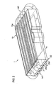
- FIGS. 1 to 9 schematically a portable data carrier 1 is shown, which, although not explicitly shown, always has an inductively coupling data communication device.
- an embodiment in map form is always used as the basis for the portable data carrier 1.
- the solutions described below are also transferable to portable data carriers 1 with other housing forms.
- the data carriers 1 are constructed on a printed circuit board 4, for example a printed circuit board, on which memory chips and a control device of the data communication device and optionally the antenna coil 2 are preferably arranged (not shown here). Furthermore, contact terminals 5 may be provided for the contact-type data exchange, which may differ depending on the data carrier type and here only in FIG. 1 are shown.
- the card-shaped data carriers 1 are micro SD cards (micro SD cards).
- the illustrated features are not limited to this type. Rather, the card-shaped data carriers 1 may also be any other card-shaped data carriers 1, in particular card-type data carriers of one of the types listed in the introduction to the description.
- the carrier substrate 3 forms the main body of the data carrier 1.
- the carrier substrate 3 can be formed, for example, by a potting compound, in particular a polymeric potting compound, into which various components of the data carrier 1, such as the memory chips and the control device, are cast.
- the data carrier 1 has the shape of a flat, cuboid body with two large top surfaces, which form a top and a bottom, and a low in comparison to the dimensions of the top surfaces peripheral edge.
- a ferritic surface 10 is formed in the form of a layer containing constituents 10a of a ferrite material.
- the ferritic surface 10, referred to below simply as a layer, has a planar design and covers most of the upper cover surface of the data carrier 1. It runs perpendicular to the coil axis of the antenna coil 2 has a plurality of elongate segments 10a which contain the ferrite material.
- the segments 10a are each separated by a gap 11 made of a dielectric material, such as a non-conductive plastic, a non-conductive paint, glass, or air, hereinafter the gap 11 is referred to as a dielectric gap.
- a ferrite material can be provided in this and all other embodiments, another material having a relative permeability ⁇ r of at least 5 and a resistivity of at least 10 -1 ⁇ m.
- the magnetic field lines MF of the magnetic field generated by the transmitting coil 2 are guided within the layer 10 along the plane of the layer 10 and directed in the longitudinal direction of the dielectric column 11, which in turn extend in the longitudinal direction of the card-shaped data carrier 1.
- the magnetic field lines MF amplified on the narrow sides of the card-shaped data carrier 1 from.
- a body 30 made of a ferrite material is further arranged within the carrier substrate 3.
- the body 30 referred to hereinafter as the ferrite body also extends in a direction parallel to the coil axis.
- the body 30 preferably has a simple geometry with a major axis and e.g. ellipsoidal or rectangular base and takes up a part of the volume of the carrier substrate. The surface of its cover sides are smaller than the surface of the layer 10, so that ferrite body 30 and layer 10 together form a T-shape in cross-section.
- the ferrite body 30 contacts the layer 10 in the sense of producing a continuous magnetic flux, ie it is connected to the layer 10 in such a way that no effective dielectric gap arises between the layer 10 and the ferrite body 30, which would disturb the magnetic flux.
- the body 30 is connected gap-free or approximately gap-free with the first layer 10.
- the body 30 physically abuts the layer 10 directly.
- body 30 and layer are approximately connected without gaps; Within these limits, a gap filled with air and / or material can also remain between the body 30 and the layer, without causing a significant deterioration of the magnetic field influencing. If a gap reaches a greater thickness, it must be filled with material with a relative permeability ⁇ r of at least 5; this is expediently done independently of the thickness.
- the above-described gap-free or approximately gap-free connection between layer 10 and body 30 is referred to below as contacting.
- ferrite material instead of the ferrite material, another material with a relative permeability ⁇ r of at least 5 and a specific electrical resistance of at least 10 -1 ⁇ m may in turn also be used for the body 30.
- the gap-free connection of the ferrite body 30 with the layer 10 creates a shielding structure which has a T-shaped longitudinal cross-section.
- This shielding structure affects the disk 1 acting or emanating from the disk 1 magnetic fields.
- Magnetic field lines MF of the magnetic alternating field generated by the coil 2 or of an incident alternating magnetic field generated by a reading device are concentrated by the ferrite body 30 and extend through the ferrite body 30 from and to the layer 10 on the upper side of the data carrier. This enhances the effect of dissipating the magnetic field lines MF in this layer 10.
- the ferrite body 30 in the direction parallel to the coil axis direction a significant extent and extending in the embodiment in the direction parallel to the coil axis direction over more than 80% of the residual height of the data carrier 1, ie the height of the data carrier 1 minus The height of the layer 10.
- the ferrite body 30 but also less, eg make up only 50% of the residual height of the data carrier 1.
- a second ferritic surface 20 extending perpendicularly or at least substantially perpendicular to the coil axis of the antenna coil 2 may also be arranged, which is likewise embodied in the form of a ferrite layer and hereinafter simply as a second layer 20 is designated.
- the second layer 20 may in turn instead of a ferrite material of another material with a relative permeability ⁇ r of at least 5 and a resistivity of at least 10 -1 ⁇ m consist.
- the second ferrite layer 20 is preferably again divided by dielectric gaps 21 into segments 20a.
- the second layer 20 is in conductive connection with the ferrite body 30, so that a shielding structure with an H-shaped cross-section is formed.
- the magnetic field lines MF are not only passed through the first layer 10 but also through the second layer 20 to the outside.
- the dielectric gaps of the second layer extend in the same direction as the dielectric gaps 11 of the first layer 10, ie in the longitudinal direction of the data carrier 1 in order to direct the magnetic field lines MF also within the second layer 20 in this direction.
- the width of the dielectric gaps 11, 21 of the first and the second layer is from 1/2 to 1/1000 of the width of the segments 10a, 20a adjoining the gaps 11, 21.
- card-shaped data carriers 1 shown are micro SD cards, in which arranged on the left side shown in the figures above electrical contacts in the form of contact surfaces 5, for illustrative purposes, however, only in FIG. 1 are explicitly drawn.
- the layer 10 is further arranged only in a region not occupied by the contacts 5 area of the data carrier 1; Accordingly, the dielectric gaps 11 of the layer 10 extend from the end of the area occupied by the contacts 5 to the opposite other end of the data carrier 1. Through the dielectric gaps 11, the magnetic field lines MF are guided within the layer 10, as explained, that they emerge from the layer 10 reinforced on the two narrow sides.
- the magnetic field lines MF in the region of the contacts 5 extend predominantly within the card-shaped data carrier 1, whereas they emerge reinforced from the data carrier 1 at the side opposite the electrical contacts 5.
- protruding in a micro SD card preferably just this narrow side of the data carrier 1 out of an opening of a read socket, so that the magnetic field lines MF on this narrow side - the so-called pull area of the micro SD card - undisturbed emerge from the opening of the read socket can.
- a perpendicular or at least substantially perpendicular to the coil axis of the antenna coil 2 extending second layer 20 may be arranged in ferrite material, which may also be segmented again.
- the second layer 20 can preferably also be arranged only in a region of the contacts 5 opposite the other end of the data carrier 1. Ideally, the body then contacts Not only the first layer 10 arranged on the upper side of the data carrier, but also the second layer 20.
- the antenna coil 2 and the first layer 10 may be disposed on one side and the second layer 20 on the opposite side of the support substrate 3, the body 30 penetrating the support substrate 3.
- FIG. 4 shown card-shaped disk 1 essentially corresponds to the FIG. 1 however, the layer 10 disposed on the surface of the data carrier 1 is not segmented. Since the layer 10 is not segmented, the magnetic field lines MF in this are not directed through dielectric gaps 11 in a preferred direction.
- the disk 1 after FIG. 4 is related to the others FIG. 1 combined aspects can be combined.
- the first layer 10 and / or the second layer 20 may be as shown in FIG FIG. 3 for the first layer 10, to be arranged only at one end of the data carrier 1, on which the magnetic field lines MF are to emerge, ie in particular on a side of the data carrier 1 opposite the electrical contacts 5.
- the ferrite body 30 extends when viewed in the direction of the coil axis only within the coil 2, which improves the effect of the ferrite body 30, since the extending through the ferrite body 30 magnetic field lines MF in amplified Measures also extend through the antenna coil 2, ie, the ferrite body 30 concentrates the magnetic field lines MF in the coil. 2
- the ferrite 30a On a - in FIG. 5 not shown - contacts 5 of the data carrier 1 opposite end of the data carrier 1 is arranged.
- This is structurally particularly favorable, since there is on this side of a micro SD card, the so-called pull-area of the card, ie an upwardly projecting portion, by means of which the micro SD card can be pulled out of a read socket.
- the pull area is presently formed by the ferrite body 30 a, which is fixed mechanically on the circuit board 4.
- the magnetic field lines MF are thereby guided by the lying on the edge of the data carrier 1 body 30a through to the arranged on the top of the data carrier layer 10. At the same time sufficient mechanical stability is achieved.
- a second ferrite layer 20 is provided on the back of the data carrier 1, but this is not mandatory.
- a dielectric gap 4 a ie, a dielectric slit formed by the circuit board 4.
- the magnetic field lines MF exit from the card-shaped data carrier 1 through this gap 4a.
- the first layer 10 arranged on the upper side of the data carrier 1 and / or the second layer 20 arranged on the rear side can be segmented, and the first layer 10 and / or the second layer 20 can, as in FIG FIG. 4 for the first Layer 10 shown to be arranged only at one end of the data carrier 1.
- the alternating magnetic fields of an external reader at the location of the data carrier 1 are strongly attenuated and generated by an antenna coil 2 of the data carrier 1 alternating magnetic fields occur only heavily attenuated to the outside, if above or below the antenna coil 2, substantially perpendicular to Coil axis of the antenna coil 2 extends a metal layer.
- This effect if the data carrier 1 is provided with the first layer 10 and / or the second layer 20 and the first layer 10 or the second layer 20 between the antenna coil 2 and the metal layer is prevented, if the first Layer 10 and / or the second layer 20 has a sufficient thickness.
- first layer 10 and optionally a second layer 20 may be provided.
- a two-sided arrangement of layers 10, 20 is particularly advantageous since the magnetic field lines MF are then guided on the top and the bottom side of the data carrier 1 in the layers 10, 20.
- the common least-area memory cards used in practice in particular micro SD cards or memory sticks, have only a very small thickness, so that, if necessary, only one-sided attachment is possible. If only a one-sided attachment is possible, the preferred arrangement for a micro SD card is usually the example in FIG. 1 illustrated arrangement of only the first layer 10 on top of the card, As a rule, there is a metal surface (eg a metal bracket) by a mechanical guide in a reading base.
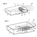
- the shielding structure is not formed by a lying on a top surface of the data carrier 1 layer 10 and a perpendicular thereto arranged simple ferrite body 30 with a single major axis, but the ferrite body has a constructed of a plurality of simple part bodies geometric shape in the at least one body part is perpendicular or substantially perpendicular to another body part.
- the parallel to the top surfaces of the data carrier 1 surfaces of the ferrite body 32, 33, 37 act as ferritic surfaces, which are segmented by the geometric shape of the body 32, 33, 37.
- One or possibly two separate ferritic surfaces or layers 10, 20, as in the embodiments of FIGS Fig. 1 to 4 may be provided in these embodiments, but are not mandatory.
- the ferrite body 32 of the shield structure in the form of a lying parallel to the top surfaces of the data carrier 1 U with a base 34 and two outgoing therefrom legs 35 is formed.
- the open side of the U is one of the narrow end faces of the data carrier 1 faces.
- the integral U-shaped ferrite body 32 may in turn be made of another material having a relative permeability ⁇ r of at least 5 and a resistivity of at least 10 -1 ⁇ m.
- the antenna coil 2 is wound in several axially spaced turns around the base of the U-shaped ferrite body 32 located between the two legs.
- the integral U-shaped body 32 is curved approximately 90 ° between the base and each of the legs.
- the integral U-shaped ferrite body 32 could in particular also be curved uniformly between the two legs by approximately 180 °, ie have a horseshoe shape.
- the magnetic field lines MF are collimated by the U-shaped ferrite body 32 and directed through the U-shaped body 32 to the both ends of the legs of the U-shaped body 32.
- the body 32 is aligned so that the legs of the body 32 extend parallel to the longitudinal sides of the data carrier 1 and the magnetic field lines MF on the opposite - not shown - electric contacts 5 narrow side of the data carrier 1 emerge from the data carrier 1.
- read pedestals in this area normally have an opening, so that the magnetic field lines MF can emerge undisturbed from this opening.
- the ferrite body 37 may also have the shape of a double U or E shape with a base 34 and three legs 35 extending therefrom, the antenna coil 2 being disposed in a plurality of axially spaced turns at least about a leg 35 or around the legs Base, preferably wrapped around the central leg of the E-shaped structure.
- the shielding structure also has a U-shaped structure.
- the U-shape is formed here of a layer 10 and an L-shaped ferrite body 33.
- the L-shaped ferrite body 33 is curved by approximately 90 ° between its base 34 and its leg 35 and makes contact with the base 34, the layer 10, wherein a dielectric gap between the layer 10 and the body 33 is to be avoided.
- the coil 2 is around the leg 35 of the L-shaped Body 33 wound because this, since it extends in the longitudinal direction of the data carrier 1, longer than dis base 34 and thus provides more space for the arrangement of the coil 2.
- the magnetic field lines MF are directed through the layer 10 and the base 34 of the L-shaped body 33 to the end of the leg 35 of the L-shaped body 33, ie the coil 2 is guided by the L-shaped body 33 to the Layer "coupled".
- the effect of the L-shaped body 33 in combination with the layer 10 is thus similar to that of the U-shaped body 32 FIG. 5 comparable, wherein the U is rotated by 90 ° about the longitudinal axis of the data carrier 10 here.
- the layer 10 is arranged in the present embodiment at the top of the data carrier 1.
- a corresponding layer 20 could be provided on the underside of the data carrier, which differs from one in comparison to FIG. 7 contacted by 180 ° rotated L-shaped body 33 is contacted.
- the leg 35 of the L-shaped body 33 terminates in a region of the other end (not shown) of the electronic contacts opposite the data carrier 1, so that the magnetic field lines MF emerge on the electrical contacts opposite narrow side of the data carrier 1.
- the layer 10 may additionally, as in the FIGS. 1 and 2 segmented by column 11 to direct the magnetic field lines MF within the layer 10 in the longitudinal direction of the column 11, preferably extending in a direction parallel to the leg 35 of the L-shaped body 33 to the magnetic field lines MF to lead in this direction.
- FIGS. 5 to 7 are the dimensions indicated for the body 32, 33, 37 for base 34 and legs 35 and their uniform dimensions with approximately square cross-section only by way of example.
- the bodies 32, 33, 37 may also be designed, for example, with rectangular or ellipsoidal cross sections, or the base 34 and legs 35 may have different dimensions.
- FIG. 8 shown card-shaped disk 1 is analogous to FIG. 7 a U-shaped structure is provided of a ferrite material, which in the present case of a first layer 10, a spaced from the first layer 10 second layer 20 and a body 30 which contacts the first and the second layer is formed.
- a corresponding U-shaped structure is previously associated with the FIGS. 3 and 4 been explained.
- the field lines MF are directed through the body 30 and the first layer 10 and the second layer 20 and are reinforced from the free ends of the two legs of the U-shaped structure 10, 20, 30, i. from the two layers 10, 20, from.
- the layers 10, 20 are arranged only in the region of the other end of the data carrier 1 (not shown), so that the magnetic field lines emerge from the data carrier 1 here.
- a corresponding recess for the body 30 is provided in the printed circuit board 4 of the data carrier 1.
- At least one of the two layers 10, 20 corresponding to the FIGS. 1 and 2 be segmented to deflect the field lines MF accordingly.
- the material of the arranged at the top of the data carrier first layer 10 and the second layer 20 and the material of the body 30, 30 a, 32, 33 of the FIGS. 1 to 8 deflects, but at the same time only slightly weakens by induced eddy currents, it has the highest possible relative permeability ⁇ r and at the same time the lowest possible electrical conductivity, ie the highest possible specific electrical resistance.
- the relative permeability ⁇ r preferably has a value of at least 100, particularly preferably at least 140, 160, 180 or even 200.
- the specific electrical resistance preferably has a value of at least 1, 10, 10 2 , 10 3 , 10 4 , 10 5 or even 10 6 ⁇ m.
- the imaginary part of the complex permeability ⁇ r ", which characterizes the magnitude of the magnetization losses in the material, is as small as possible, that is to say the magnetization losses are to be kept as small as possible
- the above values relate to the frequency range of the alternating electromagnetic field used for data transmission This is preferably 13.56 MHz.
- the material of the first layer 10 and the second layer 20 as well as the material of the bodies 30, 30a, 32, 33 can, as stated, in particular be a ferrite material. Accordingly, the first layer 10 and / or the second layer 20 may be a ferrite film, and the bodies 30, 30a, 32, 33 may be ferrite moldings.
- the highly permeable layer 40 arranged above the antenna coil 2 is formed by a polymeric potting compound 40 with ferromagnetic particles embedded therein.
- the existing of the permeable potting compound 40 layer is formed under the action of a magnetic field MF, wherein the magnetic field MF during casting and / or during the solidification process of the potting compound 40 is applied.
- Decisive for the achievable relative permeability ⁇ r is the orientation of the ferromagnetic particles within the potting compound 40.
- the ferromagnetic particles of the potting compound 40 by the magnetic field during casting and or during the solidification process in the potting compound to the outside (ie in Fig. 8 up and / or down) to thereby form a layer of increased permeability within potting compound 40.
- the potting compound has a relative permeability of at least 5.
- the potting compound consists of a material having a specific electrical resistance of at least 10 -1 ⁇ m.
- the magnetic field lines MF are passed through the potting compound 40 through to the outside.
- the magnetic field lines MF extend predominantly on the surface of the potting compound 40 at the lateral edge of the potting compound, whereas they extend downwards through the potting compound 40 and through the coil 2 in a further inner region of the potting compound 40.
- the potting compound 40 can be avoided by the potting compound 40 by a metal layer extending over the antenna coil 2, caused attenuation of the generated by an external reader electromagnetic alternating fields at the location of the antenna coil 2 and the self-generated by the antenna coil 2 itself electromagnetic alternating fields.
- the permeable potting compound 40 preferably has a relative permeability ⁇ r of at least 10, more preferably of at least 100 on.
- the aforementioned values refer to the frequency range of the alternating electromagnetic field. This is preferably 13.56 MHz.
- Second ferrite layer 20 Spaced from the potting compound 40 and on one of the potting compound 40 opposite side of the antenna coil 2 is a perpendicular or at least substantially perpendicular to the coil axis of the antenna coil 2 extending second ferrite layer 20 of a material having a relative permeability ⁇ r of at least 5 and a resistivity of at least 10 -1 ⁇ m arranged. More preferably, the material of the second layer 20 has the above-described physical properties, and more preferably, it is a ferrite material. Between the potting compound 40 and the second layer 20, a dielectric gap 4a is formed, through which the magnetic field lines MF preferably extend.
- the additional second layer 20 is not mandatory. According to a preferred embodiment, the second layer 20 can also be used in analogy to the layers 10, 20 of FIG FIGS. 1 to 3 be segmented to direct the magnetic field lines MF accordingly.
- the data communication device of the embodiments described above is particularly preferably an RFID transponder unit which operates with active load modulation, or else another radio-based data communication device which uses an active method for transmitting data.
Landscapes
- Engineering & Computer Science (AREA)
- Physics & Mathematics (AREA)
- Computer Hardware Design (AREA)
- Microelectronics & Electronic Packaging (AREA)
- General Physics & Mathematics (AREA)
- Theoretical Computer Science (AREA)
- Electromagnetism (AREA)
- Near-Field Transmission Systems (AREA)
Claims (15)
- Support de données portable (1) comportant un substrat porteur (3) et un dispositif de communication de données à couplage inductif comprenant une bobine d'antenne (2) ainsi qu'une structure de blindage influençant le champ magnétique constituée d'un matériau présentant une perméabilité relative µr d'au moins 5 et une résistance électrique spécifique d'au moins 10-1 Ωm, la structure de blindage comportant au moins une surface ferritique (10) perpendiculaire ou au moins essentiellement perpendiculaire à l'axe de bobine de la bobine d'antenne, caractérisé en ce que
la structure de blindage comporte un corps (30, 32, 33, 37) qui est agencé à l'intérieur du substrat porteur (3) et est, au moins dans un sens, parallèle à l'axe de bobine. - Support de données portable (1) selon la revendication 1,
caractérisé en ce que
la surface ferritique (10) est réalisée en tant que première couche, laquelle est subdivisée en au moins deux segments (10a) qui sont respectivement séparés l'un de l'autre par une fente (11) constituée d'un matériau diélectrique,
et en ce que le corps (30) agencé à l'intérieur du substrat porteur (3) entre en contact avec la première couche (10). - Support de données portable (1) selon la revendication 1,
caractérisé en ce que la surface ferritique (10) est réalisée en tant que première couche et en ce que, de manière espacée de la première couche (10) et d'un côté de la bobine d'antenne (2) opposé à la première couche (10), une seconde surface ferritique (20) perpendiculaire ou au moins essentiellement perpendiculaire à l'axe de bobine de la bobine d'antenne (2) est agencée, étant réalisée sous forme de seconde couche et consistant en un matériau présentant une perméabilité relative µr d'au moins 5 et une résistance électrique spécifique d'au moins 10-1 Ωm, le corps (30) entrant aussi en contact avec la seconde couche (20). - Support de données portable (1) selon la revendication 3, caractérisé en ce que la seconde couche (20) est subdivisée en au moins deux segments (20a) qui sont respectivement séparés l'un de l'autre par une fente (21) constituée d'un matériau diélectrique.
- Support de données portable (1) selon une des revendications 3 ou 4, caractérisé en ce que la bobine d'antenne (2) et la première couche (10) sont agencées d'un côté du substrat porteur (3) et en ce que la seconde couche (20) est agencée du côté opposé du substrat porteur (3), le corps (30) transperçant le substrat porteur (3).
- Support de données portable selon une des revendications de 2 à 5, caractérisé en ce que les segments (10a, 20a) sont oblongs et en ce que la largeur de la fente (11, 21) en matériau diélectrique est de 2 à 1000 fois la largeur des segments (10a, 20a) adjacents à la fente (11, 21).
- Support de données portable (1) selon une des revendications de 2, 4-6, caractérisé en ce que la fente (11, 21) en matériau diélectrique est orientée dans le sens longitudinal du support de données (1) en forme de carte.
- Support de données portable (1) selon une des revendications de 1 à 7, caractérisé en ce que, à une extrémité du support de données (1), des contacts électriques (5) sont agencés, et en ce que la surface ferritique (10) n'est agencée que dans une zone de l'autre extrémité du support de données (1) opposée aux contacts (5).
- Support de données portable (1) selon la revendication 1,
caractérisé en ce que le corps (32) est réalisé en forme de U (32; 10, 33; 10, 20, 30) avec une base (34) dont émanent deux branches (35), la base (34) étant perpendiculaire ou au moins essentiellement perpendiculaire à l'axe de bobine de la bobine d'antenne (2), et la bobine d'antenne (2) étant, en plusieurs spires axialement espacées, au moins enroulée autour d'une branche (35) ou autour de la base (34), située entre les branches, de la structure en forme de U (32; 10, 33; 10, 20, 30), et les surfaces du corps (32) parallèles aux surfaces couvrantes du support de données (1) constituant des surfaces ferritiques. - Support de données portable (1) selon la revendication 9, caractérisé en ce que la structure de blindage est un corps (32) intégral en forme de U qui est agencé parallèlement aux surfaces couvrantes du support de données (1).
- Support de données portable (1) selon la revendication 9, caractérisé en ce que le corps (37) est réalisé en forme de E avec une base (34) dont émanent trois branches (35), la bobine d'antenne (2) étant, en plusieurs spires axialement espacées, au moins enroulée autour d'une branche ou autour de la base, située entre les branches, de la structure en forme de E.
- Support de données portable (1) selon la revendication 9, caractérisé en ce que la structure (10, 33) en forme de U est constituée par une première couche (10) parallèle ou au moins essentiellement parallèle à l'axe de bobine de la bobine d'antenne (2) et par un corps (33) en forme de L qui possède une base et une branche et entre, par la branche, en contact avec la première couche (10).
- Support de données portable (1) selon une des revendications précédentes, caractérisé en ce que la surface ferritique (10) est constituée par une masse de scellement polymère (40) dans laquelle sont noyées des particules ferromagnétiques.
- Support de données portable (1) selon la revendication 13, caractérisé en ce que la masse de scellement polymère (40) est un polymère thermoplastique ou un polymère réticulant comportant des particules ferromagnétiques.
- Procédé de fabrication d'un support de données portable (1) selon la revendication 13 ou 14, caractérisé en ce que la constitution de la première couche consistant en la masse de scellement polymère (40) a lieu sous action d'un champ magnétique.
Applications Claiming Priority (2)
| Application Number | Priority Date | Filing Date | Title |
|---|---|---|---|
| DE102010005809A DE102010005809A1 (de) | 2010-01-27 | 2010-01-27 | Tragbarer Datenträger mit funkbasierter Datenkommunikationseinrichtung |
| PCT/EP2010/007545 WO2011091830A1 (fr) | 2010-01-27 | 2010-12-10 | Support de données portable avec un dispositif de radiocommunication de données |
Publications (2)
| Publication Number | Publication Date |
|---|---|
| EP2529338A1 EP2529338A1 (fr) | 2012-12-05 |
| EP2529338B1 true EP2529338B1 (fr) | 2013-11-06 |
Family
ID=43500363
Family Applications (1)
| Application Number | Title | Priority Date | Filing Date |
|---|---|---|---|
| EP10790622.4A Not-in-force EP2529338B1 (fr) | 2010-01-27 | 2010-12-10 | Support de données portable avec un dispositif de radiocommunication de données |
Country Status (3)
| Country | Link |
|---|---|
| EP (1) | EP2529338B1 (fr) |
| DE (1) | DE102010005809A1 (fr) |
| WO (1) | WO2011091830A1 (fr) |
Families Citing this family (5)
| Publication number | Priority date | Publication date | Assignee | Title |
|---|---|---|---|---|
| DE202012012880U1 (de) | 2012-08-01 | 2014-04-22 | Phoenix Contact Gmbh & Co. Kg | Spulensystem |
| DE102013104059B8 (de) * | 2013-04-22 | 2024-09-19 | Infineon Technologies Ag | Antennen-Anordnung und Kommunikationsgerät |
| WO2019007545A1 (fr) * | 2017-07-03 | 2019-01-10 | Giesecke+Devrient Mobile Security Gmbh | Support de données métallique optimisé en termes d'interférences |
| US10839274B2 (en) | 2018-04-09 | 2020-11-17 | Giesecke+Devrient Mobile Security Gmbh | Portable dual-interface data carrier with metal frame |
| DE102019210543A1 (de) | 2019-07-17 | 2021-01-21 | Aug. Winkhaus Gmbh & Co. Kg | Identifikationsmittel für eine Schließanlage |
Family Cites Families (7)
| Publication number | Priority date | Publication date | Assignee | Title |
|---|---|---|---|---|
| DE19822939A1 (de) | 1998-05-22 | 1999-11-25 | Henkel Kgaa | Nichtwäßrige viskose Geschirreinigungsmittel |
| JP4340929B2 (ja) | 1998-10-02 | 2009-10-07 | ソニー株式会社 | メモリicタグ装置 |
| DE10204884A1 (de) | 2002-02-06 | 2003-08-14 | Schreiner Gmbh & Co Kg | Transponderetikett |
| DE102004031092A1 (de) | 2004-06-28 | 2006-01-12 | Giesecke & Devrient Gmbh | Transpondereinheit |
| WO2007043626A1 (fr) * | 2005-10-14 | 2007-04-19 | International Business Machines Corporation | Étiquette rfid à induction électromagnétique et unité d’accès |
| DE102007037293A1 (de) * | 2007-08-07 | 2009-02-19 | Tagstar Systems Gmbh | Vorrichtung, Verfahren und Verwendung zur Magnetfeldabschirmung eines RFID-Transponders |
| WO2009050662A1 (fr) | 2007-10-19 | 2009-04-23 | Petratec International Ltd. | Etiquette rfid destinée à être utilisée spécialement près d'objets conducteurs |
-
2010
- 2010-01-27 DE DE102010005809A patent/DE102010005809A1/de not_active Ceased
- 2010-12-10 EP EP10790622.4A patent/EP2529338B1/fr not_active Not-in-force
- 2010-12-10 WO PCT/EP2010/007545 patent/WO2011091830A1/fr not_active Ceased
Also Published As
| Publication number | Publication date |
|---|---|
| WO2011091830A1 (fr) | 2011-08-04 |
| DE102010005809A1 (de) | 2011-07-28 |
| EP2529338A1 (fr) | 2012-12-05 |
Similar Documents
| Publication | Publication Date | Title |
|---|---|---|
| EP1745527B1 (fr) | Ensemble antenne pour la transmission inductive d'energie et utilisation dudit ensemble antenne | |
| DE102006057369A1 (de) | RFID-Etikett, sowie dessen Verwendung und ein damit gekennzeichnetes Objekt | |
| DE60221304T2 (de) | Antenne für Kartenleser | |
| DE102017130940B4 (de) | Chipkartenkörper, Chipkarte und Verfahren zum Herstellen eines Chipkartenkörpers | |
| EP2219990B1 (fr) | Chariot de manutention avec un dispositif assisté par rfid pour identifier des chargements | |
| DE102013108255A1 (de) | Chipkartenmodul mit getrennter antenne und chipkarteneinlage, die es verwendet | |
| AT514622B1 (de) | Gehäusewand | |
| EP2529338A1 (fr) | Support de données portable avec un dispositif de radiocommunication de données | |
| EP1435067A1 (fr) | Dispositif pour blinder un transpondeur, procede pour produire un blindage correspondant et transpondeur equipe de ce blindage | |
| DE102013104059B4 (de) | Antennen-Anordnung und Kommunikationsgerät | |
| EP2810222B1 (fr) | Transpondeur rfid équipé d'une antenne fendue | |
| WO2012019694A1 (fr) | Support de données portatif comprenant un dispositif de communication de données fonctionnant par l'intermédiaire d'un couplage bobine | |
| EP1956680A1 (fr) | Antenne pour lecteur de champ proche et/ou transpondeur de champ proche | |
| DE102007037293A1 (de) | Vorrichtung, Verfahren und Verwendung zur Magnetfeldabschirmung eines RFID-Transponders | |
| WO2008031630A1 (fr) | Récipient et dispositif pour détecter des objets qui se trouvent dans un espace intérieur du récipient | |
| DE102004041644A1 (de) | Transponder | |
| DE102012105437A1 (de) | RFID-Transponder mit einer invertierten F-Antenne | |
| DE102019105667A1 (de) | Booster-antenneneinrichtung | |
| EP2738715B1 (fr) | Tube Tag | |
| DE102011017168B4 (de) | Tragbarer Datenträger mit über Spulenkopplung arbeitender Datenkommunikationseinrichtung und einer Dämpfungsschicht | |
| DE102012107291B4 (de) | RFID-Tag mit polarisationsunabhängiger Antenne | |
| DE102012107561B4 (de) | RFID-Transponder mit einer planaren F-Antenne | |
| DE102011087928B4 (de) | Metallischer trägerkörper mit transponder | |
| EP4315160A1 (fr) | Corps de carte, carte à puce et procédé de fabrication d'un corps de carte pour une carte à puce | |
| EP1918860A2 (fr) | Agencement de transpondeur et procédé de fonctionnement de transpondeurs |
Legal Events
| Date | Code | Title | Description |
|---|---|---|---|
| PUAI | Public reference made under article 153(3) epc to a published international application that has entered the european phase |
Free format text: ORIGINAL CODE: 0009012 |
|
| 17P | Request for examination filed |
Effective date: 20120827 |
|
| AK | Designated contracting states |
Kind code of ref document: A1 Designated state(s): AL AT BE BG CH CY CZ DE DK EE ES FI FR GB GR HR HU IE IS IT LI LT LU LV MC MK MT NL NO PL PT RO RS SE SI SK SM TR |
|
| DAX | Request for extension of the european patent (deleted) | ||
| GRAP | Despatch of communication of intention to grant a patent |
Free format text: ORIGINAL CODE: EPIDOSNIGR1 |
|
| INTG | Intention to grant announced |
Effective date: 20130607 |
|
| GRAS | Grant fee paid |
Free format text: ORIGINAL CODE: EPIDOSNIGR3 |
|
| GRAA | (expected) grant |
Free format text: ORIGINAL CODE: 0009210 |
|
| AK | Designated contracting states |
Kind code of ref document: B1 Designated state(s): AL AT BE BG CH CY CZ DE DK EE ES FI FR GB GR HR HU IE IS IT LI LT LU LV MC MK MT NL NO PL PT RO RS SE SI SK SM TR |
|
| REG | Reference to a national code |
Ref country code: GB Ref legal event code: FG4D Free format text: NOT ENGLISH |
|
| REG | Reference to a national code |
Ref country code: CH Ref legal event code: EP |
|
| REG | Reference to a national code |
Ref country code: AT Ref legal event code: REF Ref document number: 639903 Country of ref document: AT Kind code of ref document: T Effective date: 20131215 |
|
| REG | Reference to a national code |
Ref country code: IE Ref legal event code: FG4D Free format text: LANGUAGE OF EP DOCUMENT: GERMAN |
|
| REG | Reference to a national code |
Ref country code: DE Ref legal event code: R096 Ref document number: 502010005342 Country of ref document: DE Effective date: 20140102 |
|
| REG | Reference to a national code |
Ref country code: NL Ref legal event code: VDEP Effective date: 20131106 |
|
| REG | Reference to a national code |
Ref country code: LT Ref legal event code: MG4D |
|
| PG25 | Lapsed in a contracting state [announced via postgrant information from national office to epo] |
Ref country code: LT Free format text: LAPSE BECAUSE OF FAILURE TO SUBMIT A TRANSLATION OF THE DESCRIPTION OR TO PAY THE FEE WITHIN THE PRESCRIBED TIME-LIMIT Effective date: 20131106 Ref country code: HR Free format text: LAPSE BECAUSE OF FAILURE TO SUBMIT A TRANSLATION OF THE DESCRIPTION OR TO PAY THE FEE WITHIN THE PRESCRIBED TIME-LIMIT Effective date: 20131106 Ref country code: SE Free format text: LAPSE BECAUSE OF FAILURE TO SUBMIT A TRANSLATION OF THE DESCRIPTION OR TO PAY THE FEE WITHIN THE PRESCRIBED TIME-LIMIT Effective date: 20131106 Ref country code: IS Free format text: LAPSE BECAUSE OF FAILURE TO SUBMIT A TRANSLATION OF THE DESCRIPTION OR TO PAY THE FEE WITHIN THE PRESCRIBED TIME-LIMIT Effective date: 20140306 Ref country code: FI Free format text: LAPSE BECAUSE OF FAILURE TO SUBMIT A TRANSLATION OF THE DESCRIPTION OR TO PAY THE FEE WITHIN THE PRESCRIBED TIME-LIMIT Effective date: 20131106 Ref country code: NO Free format text: LAPSE BECAUSE OF FAILURE TO SUBMIT A TRANSLATION OF THE DESCRIPTION OR TO PAY THE FEE WITHIN THE PRESCRIBED TIME-LIMIT Effective date: 20140206 Ref country code: NL Free format text: LAPSE BECAUSE OF FAILURE TO SUBMIT A TRANSLATION OF THE DESCRIPTION OR TO PAY THE FEE WITHIN THE PRESCRIBED TIME-LIMIT Effective date: 20131106 |
|
| PG25 | Lapsed in a contracting state [announced via postgrant information from national office to epo] |
Ref country code: ES Free format text: LAPSE BECAUSE OF FAILURE TO SUBMIT A TRANSLATION OF THE DESCRIPTION OR TO PAY THE FEE WITHIN THE PRESCRIBED TIME-LIMIT Effective date: 20131106 Ref country code: LV Free format text: LAPSE BECAUSE OF FAILURE TO SUBMIT A TRANSLATION OF THE DESCRIPTION OR TO PAY THE FEE WITHIN THE PRESCRIBED TIME-LIMIT Effective date: 20131106 Ref country code: RS Free format text: LAPSE BECAUSE OF FAILURE TO SUBMIT A TRANSLATION OF THE DESCRIPTION OR TO PAY THE FEE WITHIN THE PRESCRIBED TIME-LIMIT Effective date: 20131106 |
|
| BERE | Be: lapsed |
Owner name: GIESECKE & DEVRIENT G.M.B.H. Effective date: 20131231 |
|
| PG25 | Lapsed in a contracting state [announced via postgrant information from national office to epo] |
Ref country code: PT Free format text: LAPSE BECAUSE OF FAILURE TO SUBMIT A TRANSLATION OF THE DESCRIPTION OR TO PAY THE FEE WITHIN THE PRESCRIBED TIME-LIMIT Effective date: 20140306 |
|
| PG25 | Lapsed in a contracting state [announced via postgrant information from national office to epo] |
Ref country code: EE Free format text: LAPSE BECAUSE OF FAILURE TO SUBMIT A TRANSLATION OF THE DESCRIPTION OR TO PAY THE FEE WITHIN THE PRESCRIBED TIME-LIMIT Effective date: 20131106 |
|
| REG | Reference to a national code |
Ref country code: DE Ref legal event code: R097 Ref document number: 502010005342 Country of ref document: DE |
|
| PG25 | Lapsed in a contracting state [announced via postgrant information from national office to epo] |
Ref country code: SK Free format text: LAPSE BECAUSE OF FAILURE TO SUBMIT A TRANSLATION OF THE DESCRIPTION OR TO PAY THE FEE WITHIN THE PRESCRIBED TIME-LIMIT Effective date: 20131106 Ref country code: PL Free format text: LAPSE BECAUSE OF FAILURE TO SUBMIT A TRANSLATION OF THE DESCRIPTION OR TO PAY THE FEE WITHIN THE PRESCRIBED TIME-LIMIT Effective date: 20131106 Ref country code: RO Free format text: LAPSE BECAUSE OF FAILURE TO SUBMIT A TRANSLATION OF THE DESCRIPTION OR TO PAY THE FEE WITHIN THE PRESCRIBED TIME-LIMIT Effective date: 20131106 Ref country code: IT Free format text: LAPSE BECAUSE OF FAILURE TO SUBMIT A TRANSLATION OF THE DESCRIPTION OR TO PAY THE FEE WITHIN THE PRESCRIBED TIME-LIMIT Effective date: 20131106 Ref country code: CZ Free format text: LAPSE BECAUSE OF FAILURE TO SUBMIT A TRANSLATION OF THE DESCRIPTION OR TO PAY THE FEE WITHIN THE PRESCRIBED TIME-LIMIT Effective date: 20131106 |
|
| PLBE | No opposition filed within time limit |
Free format text: ORIGINAL CODE: 0009261 |
|
| STAA | Information on the status of an ep patent application or granted ep patent |
Free format text: STATUS: NO OPPOSITION FILED WITHIN TIME LIMIT |
|
| REG | Reference to a national code |
Ref country code: IE Ref legal event code: MM4A |
|
| PG25 | Lapsed in a contracting state [announced via postgrant information from national office to epo] |
Ref country code: DK Free format text: LAPSE BECAUSE OF FAILURE TO SUBMIT A TRANSLATION OF THE DESCRIPTION OR TO PAY THE FEE WITHIN THE PRESCRIBED TIME-LIMIT Effective date: 20131106 |
|
| 26N | No opposition filed |
Effective date: 20140807 |
|
| PG25 | Lapsed in a contracting state [announced via postgrant information from national office to epo] |
Ref country code: IE Free format text: LAPSE BECAUSE OF NON-PAYMENT OF DUE FEES Effective date: 20131210 Ref country code: BE Free format text: LAPSE BECAUSE OF NON-PAYMENT OF DUE FEES Effective date: 20131231 |
|
| REG | Reference to a national code |
Ref country code: DE Ref legal event code: R097 Ref document number: 502010005342 Country of ref document: DE Effective date: 20140807 |
|
| PG25 | Lapsed in a contracting state [announced via postgrant information from national office to epo] |
Ref country code: SI Free format text: LAPSE BECAUSE OF FAILURE TO SUBMIT A TRANSLATION OF THE DESCRIPTION OR TO PAY THE FEE WITHIN THE PRESCRIBED TIME-LIMIT Effective date: 20131106 |
|
| PG25 | Lapsed in a contracting state [announced via postgrant information from national office to epo] |
Ref country code: MC Free format text: LAPSE BECAUSE OF FAILURE TO SUBMIT A TRANSLATION OF THE DESCRIPTION OR TO PAY THE FEE WITHIN THE PRESCRIBED TIME-LIMIT Effective date: 20131106 |
|
| PG25 | Lapsed in a contracting state [announced via postgrant information from national office to epo] |
Ref country code: SM Free format text: LAPSE BECAUSE OF FAILURE TO SUBMIT A TRANSLATION OF THE DESCRIPTION OR TO PAY THE FEE WITHIN THE PRESCRIBED TIME-LIMIT Effective date: 20131106 |
|
| PG25 | Lapsed in a contracting state [announced via postgrant information from national office to epo] |
Ref country code: CY Free format text: LAPSE BECAUSE OF FAILURE TO SUBMIT A TRANSLATION OF THE DESCRIPTION OR TO PAY THE FEE WITHIN THE PRESCRIBED TIME-LIMIT Effective date: 20131106 |
|
| PG25 | Lapsed in a contracting state [announced via postgrant information from national office to epo] |
Ref country code: LU Free format text: LAPSE BECAUSE OF NON-PAYMENT OF DUE FEES Effective date: 20131210 Ref country code: HU Free format text: LAPSE BECAUSE OF FAILURE TO SUBMIT A TRANSLATION OF THE DESCRIPTION OR TO PAY THE FEE WITHIN THE PRESCRIBED TIME-LIMIT; INVALID AB INITIO Effective date: 20101210 Ref country code: MK Free format text: LAPSE BECAUSE OF FAILURE TO SUBMIT A TRANSLATION OF THE DESCRIPTION OR TO PAY THE FEE WITHIN THE PRESCRIBED TIME-LIMIT Effective date: 20131106 Ref country code: BG Free format text: LAPSE BECAUSE OF FAILURE TO SUBMIT A TRANSLATION OF THE DESCRIPTION OR TO PAY THE FEE WITHIN THE PRESCRIBED TIME-LIMIT Effective date: 20131106 |
|
| REG | Reference to a national code |
Ref country code: CH Ref legal event code: PL |
|
| PG25 | Lapsed in a contracting state [announced via postgrant information from national office to epo] |
Ref country code: GR Free format text: LAPSE BECAUSE OF NON-PAYMENT OF DUE FEES Effective date: 20131106 Ref country code: MT Free format text: LAPSE BECAUSE OF FAILURE TO SUBMIT A TRANSLATION OF THE DESCRIPTION OR TO PAY THE FEE WITHIN THE PRESCRIBED TIME-LIMIT Effective date: 20131106 |
|
| PG25 | Lapsed in a contracting state [announced via postgrant information from national office to epo] |
Ref country code: CH Free format text: LAPSE BECAUSE OF NON-PAYMENT OF DUE FEES Effective date: 20141231 Ref country code: LI Free format text: LAPSE BECAUSE OF NON-PAYMENT OF DUE FEES Effective date: 20141231 |
|
| REG | Reference to a national code |
Ref country code: FR Ref legal event code: PLFP Year of fee payment: 6 |
|
| PG25 | Lapsed in a contracting state [announced via postgrant information from national office to epo] |
Ref country code: GR Free format text: LAPSE BECAUSE OF FAILURE TO SUBMIT A TRANSLATION OF THE DESCRIPTION OR TO PAY THE FEE WITHIN THE PRESCRIBED TIME-LIMIT Effective date: 20140207 |
|
| PG25 | Lapsed in a contracting state [announced via postgrant information from national office to epo] |
Ref country code: TR Free format text: LAPSE BECAUSE OF FAILURE TO SUBMIT A TRANSLATION OF THE DESCRIPTION OR TO PAY THE FEE WITHIN THE PRESCRIBED TIME-LIMIT Effective date: 20131106 |
|
| REG | Reference to a national code |
Ref country code: FR Ref legal event code: PLFP Year of fee payment: 7 |
|
| REG | Reference to a national code |
Ref country code: AT Ref legal event code: MM01 Ref document number: 639903 Country of ref document: AT Kind code of ref document: T Effective date: 20151210 |
|
| PG25 | Lapsed in a contracting state [announced via postgrant information from national office to epo] |
Ref country code: AT Free format text: LAPSE BECAUSE OF NON-PAYMENT OF DUE FEES Effective date: 20151210 |
|
| REG | Reference to a national code |
Ref country code: DE Ref legal event code: R081 Ref document number: 502010005342 Country of ref document: DE Owner name: GIESECKE+DEVRIENT MOBILE SECURITY GMBH, DE Free format text: FORMER OWNER: GIESECKE & DEVRIENT GMBH, 81677 MUENCHEN, DE |
|
| REG | Reference to a national code |
Ref country code: FR Ref legal event code: PLFP Year of fee payment: 8 |
|
| REG | Reference to a national code |
Ref country code: GB Ref legal event code: 732E Free format text: REGISTERED BETWEEN 20180118 AND 20180124 |
|
| REG | Reference to a national code |
Ref country code: FR Ref legal event code: TP Owner name: GIESECKE+DEVRIENT MOBILE SECURITY GMBH, DE Effective date: 20180619 |
|
| PG25 | Lapsed in a contracting state [announced via postgrant information from national office to epo] |
Ref country code: AL Free format text: LAPSE BECAUSE OF FAILURE TO SUBMIT A TRANSLATION OF THE DESCRIPTION OR TO PAY THE FEE WITHIN THE PRESCRIBED TIME-LIMIT Effective date: 20131106 |
|
| P01 | Opt-out of the competence of the unified patent court (upc) registered |
Effective date: 20230520 |
|
| REG | Reference to a national code |
Ref country code: DE Ref legal event code: R081 Ref document number: 502010005342 Country of ref document: DE Owner name: GIESECKE+DEVRIENT EPAYMENTS GMBH, DE Free format text: FORMER OWNER: GIESECKE+DEVRIENT MOBILE SECURITY GMBH, 81677 MUENCHEN, DE |
|
| PGFP | Annual fee paid to national office [announced via postgrant information from national office to epo] |
Ref country code: GB Payment date: 20231220 Year of fee payment: 14 |
|
| PGFP | Annual fee paid to national office [announced via postgrant information from national office to epo] |
Ref country code: FR Payment date: 20231220 Year of fee payment: 14 Ref country code: DE Payment date: 20231231 Year of fee payment: 14 |
|
| REG | Reference to a national code |
Ref country code: DE Ref legal event code: R119 Ref document number: 502010005342 Country of ref document: DE |
|
| GBPC | Gb: european patent ceased through non-payment of renewal fee |
Effective date: 20241210 |
|
| PG25 | Lapsed in a contracting state [announced via postgrant information from national office to epo] |
Ref country code: DE Free format text: LAPSE BECAUSE OF NON-PAYMENT OF DUE FEES Effective date: 20250701 |
|
| PG25 | Lapsed in a contracting state [announced via postgrant information from national office to epo] |
Ref country code: GB Free format text: LAPSE BECAUSE OF NON-PAYMENT OF DUE FEES Effective date: 20241210 |
|
| PG25 | Lapsed in a contracting state [announced via postgrant information from national office to epo] |
Ref country code: FR Free format text: LAPSE BECAUSE OF NON-PAYMENT OF DUE FEES Effective date: 20241231 |