EP2529418B1 - Procede de realisation d'une cellule photovoltaique avec preparation de surface d'un substrat en silicium cristallin - Google Patents
Procede de realisation d'une cellule photovoltaique avec preparation de surface d'un substrat en silicium cristallin Download PDFInfo
- Publication number
- EP2529418B1 EP2529418B1 EP11708520.9A EP11708520A EP2529418B1 EP 2529418 B1 EP2529418 B1 EP 2529418B1 EP 11708520 A EP11708520 A EP 11708520A EP 2529418 B1 EP2529418 B1 EP 2529418B1
- Authority
- EP
- European Patent Office
- Prior art keywords
- substrate
- silicon oxide
- silicon
- layer
- thin film
- Prior art date
- Legal status (The legal status is an assumption and is not a legal conclusion. Google has not performed a legal analysis and makes no representation as to the accuracy of the status listed.)
- Active
Links
Images



Classifications
-
- H—ELECTRICITY
- H10—SEMICONDUCTOR DEVICES; ELECTRIC SOLID-STATE DEVICES NOT OTHERWISE PROVIDED FOR
- H10F—INORGANIC SEMICONDUCTOR DEVICES SENSITIVE TO INFRARED RADIATION, LIGHT, ELECTROMAGNETIC RADIATION OF SHORTER WAVELENGTH OR CORPUSCULAR RADIATION
- H10F77/00—Constructional details of devices covered by this subclass
- H10F77/70—Surface textures, e.g. pyramid structures
- H10F77/703—Surface textures, e.g. pyramid structures of the semiconductor bodies, e.g. textured active layers
-
- H—ELECTRICITY
- H10—SEMICONDUCTOR DEVICES; ELECTRIC SOLID-STATE DEVICES NOT OTHERWISE PROVIDED FOR
- H10P—GENERIC PROCESSES OR APPARATUS FOR THE MANUFACTURE OR TREATMENT OF DEVICES COVERED BY CLASS H10
- H10P50/00—Etching of wafers, substrates or parts of devices
- H10P50/60—Wet etching
- H10P50/64—Wet etching of semiconductor materials
- H10P50/642—Chemical etching
-
- H—ELECTRICITY
- H10—SEMICONDUCTOR DEVICES; ELECTRIC SOLID-STATE DEVICES NOT OTHERWISE PROVIDED FOR
- H10F—INORGANIC SEMICONDUCTOR DEVICES SENSITIVE TO INFRARED RADIATION, LIGHT, ELECTROMAGNETIC RADIATION OF SHORTER WAVELENGTH OR CORPUSCULAR RADIATION
- H10F10/00—Individual photovoltaic cells, e.g. solar cells
- H10F10/10—Individual photovoltaic cells, e.g. solar cells having potential barriers
- H10F10/17—Photovoltaic cells having only PIN junction potential barriers
-
- H—ELECTRICITY
- H10—SEMICONDUCTOR DEVICES; ELECTRIC SOLID-STATE DEVICES NOT OTHERWISE PROVIDED FOR
- H10F—INORGANIC SEMICONDUCTOR DEVICES SENSITIVE TO INFRARED RADIATION, LIGHT, ELECTROMAGNETIC RADIATION OF SHORTER WAVELENGTH OR CORPUSCULAR RADIATION
- H10F71/00—Manufacture or treatment of devices covered by this subclass
-
- H—ELECTRICITY
- H10—SEMICONDUCTOR DEVICES; ELECTRIC SOLID-STATE DEVICES NOT OTHERWISE PROVIDED FOR
- H10F—INORGANIC SEMICONDUCTOR DEVICES SENSITIVE TO INFRARED RADIATION, LIGHT, ELECTROMAGNETIC RADIATION OF SHORTER WAVELENGTH OR CORPUSCULAR RADIATION
- H10F71/00—Manufacture or treatment of devices covered by this subclass
- H10F71/10—Manufacture or treatment of devices covered by this subclass the devices comprising amorphous semiconductor material
- H10F71/103—Manufacture or treatment of devices covered by this subclass the devices comprising amorphous semiconductor material including only Group IV materials
-
- H—ELECTRICITY
- H10—SEMICONDUCTOR DEVICES; ELECTRIC SOLID-STATE DEVICES NOT OTHERWISE PROVIDED FOR
- H10F—INORGANIC SEMICONDUCTOR DEVICES SENSITIVE TO INFRARED RADIATION, LIGHT, ELECTROMAGNETIC RADIATION OF SHORTER WAVELENGTH OR CORPUSCULAR RADIATION
- H10F77/00—Constructional details of devices covered by this subclass
- H10F77/10—Semiconductor bodies
- H10F77/16—Material structures, e.g. crystalline structures, film structures or crystal plane orientations
- H10F77/162—Non-monocrystalline materials, e.g. semiconductor particles embedded in insulating materials
-
- H—ELECTRICITY
- H10—SEMICONDUCTOR DEVICES; ELECTRIC SOLID-STATE DEVICES NOT OTHERWISE PROVIDED FOR
- H10F—INORGANIC SEMICONDUCTOR DEVICES SENSITIVE TO INFRARED RADIATION, LIGHT, ELECTROMAGNETIC RADIATION OF SHORTER WAVELENGTH OR CORPUSCULAR RADIATION
- H10F77/00—Constructional details of devices covered by this subclass
- H10F77/10—Semiconductor bodies
- H10F77/16—Material structures, e.g. crystalline structures, film structures or crystal plane orientations
- H10F77/162—Non-monocrystalline materials, e.g. semiconductor particles embedded in insulating materials
- H10F77/164—Polycrystalline semiconductors
- H10F77/1642—Polycrystalline semiconductors including only Group IV materials
- H10F77/1645—Polycrystalline semiconductors including only Group IV materials including microcrystalline silicon
-
- Y—GENERAL TAGGING OF NEW TECHNOLOGICAL DEVELOPMENTS; GENERAL TAGGING OF CROSS-SECTIONAL TECHNOLOGIES SPANNING OVER SEVERAL SECTIONS OF THE IPC; TECHNICAL SUBJECTS COVERED BY FORMER USPC CROSS-REFERENCE ART COLLECTIONS [XRACs] AND DIGESTS
- Y02—TECHNOLOGIES OR APPLICATIONS FOR MITIGATION OR ADAPTATION AGAINST CLIMATE CHANGE
- Y02E—REDUCTION OF GREENHOUSE GAS [GHG] EMISSIONS, RELATED TO ENERGY GENERATION, TRANSMISSION OR DISTRIBUTION
- Y02E10/00—Energy generation through renewable energy sources
- Y02E10/50—Photovoltaic [PV] energy
- Y02E10/545—Microcrystalline silicon PV cells
-
- Y—GENERAL TAGGING OF NEW TECHNOLOGICAL DEVELOPMENTS; GENERAL TAGGING OF CROSS-SECTIONAL TECHNOLOGIES SPANNING OVER SEVERAL SECTIONS OF THE IPC; TECHNICAL SUBJECTS COVERED BY FORMER USPC CROSS-REFERENCE ART COLLECTIONS [XRACs] AND DIGESTS
- Y02—TECHNOLOGIES OR APPLICATIONS FOR MITIGATION OR ADAPTATION AGAINST CLIMATE CHANGE
- Y02E—REDUCTION OF GREENHOUSE GAS [GHG] EMISSIONS, RELATED TO ENERGY GENERATION, TRANSMISSION OR DISTRIBUTION
- Y02E10/00—Energy generation through renewable energy sources
- Y02E10/50—Photovoltaic [PV] energy
- Y02E10/548—Amorphous silicon PV cells
-
- Y—GENERAL TAGGING OF NEW TECHNOLOGICAL DEVELOPMENTS; GENERAL TAGGING OF CROSS-SECTIONAL TECHNOLOGIES SPANNING OVER SEVERAL SECTIONS OF THE IPC; TECHNICAL SUBJECTS COVERED BY FORMER USPC CROSS-REFERENCE ART COLLECTIONS [XRACs] AND DIGESTS
- Y02—TECHNOLOGIES OR APPLICATIONS FOR MITIGATION OR ADAPTATION AGAINST CLIMATE CHANGE
- Y02P—CLIMATE CHANGE MITIGATION TECHNOLOGIES IN THE PRODUCTION OR PROCESSING OF GOODS
- Y02P70/00—Climate change mitigation technologies in the production process for final industrial or consumer products
- Y02P70/50—Manufacturing or production processes characterised by the final manufactured product
Definitions
- a photovoltaic cell is formed of a multilayer stack for directly converting the received photons into an electrical signal.
- Such a photovoltaic cell may, for example, be a heterojunction photovoltaic cell.
- the heterojunction is, in particular, formed by a crystalline silicon substrate having a given type of doping (n or p) and an amorphous silicon layer having a type opposite to that of the substrate.
- an intermediate layer called "passivation" is most often disposed between the two elements forming the heterojunction, in order to improve the interface characteristics of the heterojunction and therefore the efficiency of the conversion.
- this intermediate layer is, in general, an intrinsic amorphous silicon layer.
- the front face 1a of the substrate 1 is, in addition, textured (or structured), in order to increase the optical confinement of the cell.
- photovoltaic cells such as heterojunction photovoltaic cells as illustrated in FIGS. Figures 1 and 2 , require to deposit, in a uniform manner, a plurality of very thin layers (of the order of a few nanometers to a few tens of nanometers) on a substrate of which at least one face is textured.
- uniform deposition also called compliant deposition by some
- a thin layer is understood to mean the deposition of a thin layer of a substantially constant thickness, in order to follow the relief of the face on which the thin layer is deposited.
- the texturing step of the substrate of at least one face does not facilitate the proper conformation (or uniform distribution) of these layers.
- the texturing is advantageously carried out by at least one anisotropic etching step with the aid of an alkaline solution, such as potassium hydroxide (KOH) or sodium hydroxide (NaOH). It has also been proposed to add an active interface agent, such as isopropyl alcohol (IPA) to the alkaline solution, in order to limit the roughness phenomenon.
- KOH potassium hydroxide
- NaOH sodium hydroxide
- IPA isopropyl alcohol
- the substrate 1 is textured by performing a cleaning of the surface and then dipping the cleaned substrate in an alkaline solution, such as NaOH which is optionally added isopropyl alcohol (IPA) to perform the anisotropic etching.
- an alkaline solution such as NaOH which is optionally added isopropyl alcohol (IPA) to perform the anisotropic etching.
- the patent application US2001 / 0029978 proposes also to follow the step of anisotropic etching by a step intended to round the zones arranged between two pyramids (zones "b" on the figure 1 ) formed during the anisotropic etching step.
- the substrate undergoes a series of cleaning steps, before being subjected to an isotropic etching step, by immersion in an aqueous solution containing hydrofluoric acid (HF) and nitric acid (HNO 3 ) in a 1:20 ratio for about 30 seconds. Subsequently, the substrate undergoes cleaning steps (deionized water also denoted DI water, then HF + water, then DI water).
- the isotropic etching step with the mixture of HF and HNO 3 makes it possible, in known manner, to form a silicon oxide by virtue of the oxidizing action of the nitric acid and to etch off said oxide. of silicon by the attacking action of hydrofluoric acid.
- the aqueous mixture may also contain CH 3 COOH.
- the wet isotropic etching proposed in the patent application US2001 / 0029978 is, however, too important (of the order of 2 ⁇ m or more). It does not therefore make it possible to obtain a smoothing of the flanks of the pyramids at the nanometric level, nor even to round the peaks of the pyramids.
- the production of photovoltaic cells comprises a surface texturing step to form patterns in the form of pyramids, for example.
- the process described in the patent application WO-A-2009/120631 may also include a post-cleaning step performed by an oxidation operation of the surface, followed by an etching operation.
- the oxidation operation is carried out chemically, by immersion in a liquid solution such as a deionized water bath comprising between 1 ppm and 30 ppm of ozone, with possibly 1% by volume of HCl. This chemical oxidation operation then generates a very fine oxide, inhomogeneous in thickness on the surface textured to treat.
- etching removal of such an oxide is sufficient to achieve a surface cleaning, but remains insufficient to obtain a smoothing texturing, whose purpose is to round or soften the corners of the texture. That's why in the patent application WO-2009/12631 a specific step of smoothing is, in particular, performed before this post-cleaning step, when it is desired to round or soften the angles of the texturing performed. This optional step of smoothing is, as in the patent application US2001 / 0029978 , carried out wet, with the disadvantages described above.
- the object of the invention is to propose, for a method for producing at least one photovoltaic cell, an isotropic etching treatment that makes it possible to improve the surface condition of the crystalline silicon substrate once said etched surface has been anisotropically etched, compared to the isotropic etching treatments proposed according to the prior art.
- the object of the invention is to obtain, for a surface of a textured substrate in the form of pyramids, a rounding of the vertices and zones arranged between two pyramids as well as a smoothing of the flanks of said pyramids.
- the two successive operations constitute a repeated operational cycle at least once during the isotropic etching treatment.
- the anisotropic etching of the front face 1a of the substrate 1 makes it possible to structure (or texture) the front face 1a in the form of pyramids. It is, for example, carried out by immersing the face 1a of the substrate 1 in an aqueous anisotropic etching solution, containing potassium hydroxide (KOH) and isopropyl alcohol (IPA), for 30 minutes and at a temperature of of 80 ° C.
- KOH potassium hydroxide
- IPA isopropyl alcohol
- the rear face 1b may be covered with a protective mask (for example SiO 2 or Si 3 N 4 ) resistant to anisotropic etching carried out with the aqueous solution containing KOH in order to preserve said rear face 1b.
- a protective mask for example SiO 2 or Si 3 N 4
- anisotropic etching carried out with the aqueous solution containing KOH in order to preserve said rear face 1b.
- the flanks "f" of the pyramids obtained form, in general, an angle of 54.7 ° with the main "P" plane of the face 1a, that is to say the plane of the face 1a before it is textured.
- the widths of the pyramids are between 0.1 ⁇ m and 40 ⁇ m and advantageously between 1 ⁇ m and 30 ⁇ m , depending on the concentration of the aqueous solution and the etching time.
- the surface state of said face 1a after the anisotropic etching operation and, in particular, the flanks "f" of the pyramids are rough (schematized by the dashed lines on the figure 5 ) and the vertices "s" of the pyramids, just as the zones "b” arranged between two pyramids, are steep (with, in particular, a radius of curvature less than 30 nm).
- an isotropic etching treatment comprising at least two successive operations respectively consisting in forming a silicon oxide thin film of a controlled thickness and in removing said thin film thus formed, preferably in a homogeneous manner.
- the thickness of the silicon oxide thin film is, in addition, between 2 nm and 500 nm and is preferably homogeneous on at least the flanks "f" of the pyramids and advantageously over the entire surface treated.
- the formation of a thin film of silicon oxide on the face 1a of the substrate 1 is carried out by a thermally activated dry oxidation process, that is to say by oxidizing the face of the substrate by means of a non-liquid oxidizing agent while maintaining said face at a temperature above ambient temperature.
- the oxidizing agent may, in particular, be in gaseous form or be contained in a plasma. It may, for example, be oxygen, ozone, water, alone or in mixture.
- the thermal activation of the oxidation by the dry route consists in supplying energy to the face of the substrate, by applying a thermal budget defined by at least a temperature higher than the ambient temperature and advantageously greater than or equal to 40 ° C.
- such a thermal budget is advantageously adapted to make it possible to obtain a compromise between a rapid rise in temperature and sufficiently high to generate the silicon oxide thin film and to obtain a final temperature not too high for avoid an alteration of the surface or volume properties of the silicon substrate.
- the treatment also eliminates much of the particulate contamination, which is particularly critical on textured silicon substrates.
- the isotropic etching treatment can be carried out in different ways.
- the thermally activated dry oxidation process can be a thermal oxidation, that is to say an oxidation by means of at least one oxidizing agent in gaseous form or contained in a plasma and by application to the substrate face with a temperature above room temperature and preferably greater than or equal to 40 ° C.
- the applied temperature is less than 1100 ° C.
- a rapid process of treatment also known under the name of "Rapid Thermal Process” or the acronym "RTP”
- the dry oxidation operation is preferably carried out with a very rapid temperature rise (for example between 100 ° C./s and 200 ° C./s).
- the final temperature obtained at the end of this rise in temperature is preferably moderate in order to avoid damage to the treated surface state and the volume properties of the substrate.
- the thermally activated dry oxidation process can also be assisted or it can be obtained by application of radiation ultraviolet rays having a wavelength in the range of 0.15 ⁇ m to 0.4 ⁇ m and preferably about 254 nm and about 185 nm.
- a plasma treatment activated for example by radiofrequency, microwave or microwave.
- the plasma may, for example, be a plasma, such as an inductive plasma or an ionic reactive etching plasma (RIE).
- the oxidizing agent may be a gas or a mixture of gases that may contain oxygen, ozone, water vapor or it may be another gaseous oxidizing species, alone or in combination, in a form molecular, ionic, radical or atomic.
- the total pressure during the oxidation operation can be of any type: it can be atmospheric, sub-atmospheric or over-atmospheric. It is also possible to vary the partial pressure or pressures of each species constituting the oxidizing agent as a function of the total pressure. In particular, the partial pressure (s) of each species may be adjusted according to the desired oxidation rate.
- the oxidation operation may be a thermal oxidation carried out with a temperature of the order of 400 ° C., with a gas mixture of oxygen and ozone (in particular from 3 to 4% of O 3 with respect to O 2 ).
- a gas mixture of oxygen and ozone in particular from 3 to 4% of O 3 with respect to O 2 .
- Such an operation makes it possible to obtain a thin film of silicon oxide having a thickness sufficient to improve the surface state, once said film has been removed.
- a thickness greater than 10 nm which can be obtained for example with a temperature of 450 ° C. for 3 hours, will be chosen. Larger thicknesses can be obtained by increasing the temperature and / or the treatment time. For example, 25 nm of silicon oxide can be obtained with a temperature of 550 ° C for 4 hours.
- the oxide thickness of silicon is multiplied by four compared to a film obtained by oxidation with only oxygen at the same temperature.
- the oxidation operation may be a thermal oxidation carried out between 700 ° C. and 800 ° C., assisted by UV radiation in a gaseous mixture of oxygen and ozone (approximately 2 ppm of O 3 relative to at O 2 ).
- a thermal oxidation carried out between 700 ° C. and 800 ° C., assisted by UV radiation in a gaseous mixture of oxygen and ozone (approximately 2 ppm of O 3 relative to at O 2 ).
- a gaseous mixture of oxygen and ozone approximately 2 ppm of O 3 relative to at O 2 .
- Such an operation makes it possible to obtain a thin film of silicon oxide having a thickness sufficient to improve the surface state, once said film has been removed.
- the thickness of silicon oxide is increased from 50% to 100% with respect to a film obtained by oxidation with only oxygen.
- the thickness of silicon oxide generated will advantageously be chosen to be greater than 10 nm. For example, with oxidation at 800 ° C. for 140
- a film of 60 nm thickness is obtained at 900 ° C. and from 5 nm to 700 ° C.
- the thickness of silicon oxide generated during the isotropic etching treatment operation can also be increased by an operational cycle formed by the successive oxidation and removal operations, as will be detailed later.
- the oxidation operation may be an oxidation obtained by microwave activated plasma treatment (2,45GHz) and assisted by DC-magnetron polarization (100V) and with a partial oxygen pressure. about 100mT.
- the oxide thin film formed has a thickness of about 400 nm for an oxidation time of one hour, on a surface of a silicon wafer whose surface temperature is maintained at about 600. ° C.
- the removal operation of the thin film of silicon oxide, directly following the oxidation operation, may be carried out by the dry route, for example by reactive ion etching (RIE) or by wet process, for example by immersing the side 1a of the substrate 1 in a liquid solution containing hydrochloric acid (HCl) and optionally hydrofluoric acid (HF) (BHF).
- RIE reactive ion etching
- BHF hydrofluoric acid
- the removal operation can also be carried out by treatment in a reducing medium, for example by carrying out a thermal treatment under hydrogen.
- These exemplary shrinkage steps are known to be homogeneous shrinkage steps, i.e. shrinkage with a constant shrinkage speed on the underside of the surface, despite texturing.
- the two successive operations constitute an operational cycle that is repeated at least once.
- Such a repetition is particularly advantageous when the thin film made of silicon oxide has a thickness of the order of 2 nm.
- the repetition of the two successive operations of oxidation and removal of the silicon oxide thin film makes it possible to optimize the process and in particular to obtain a saving of time.
- the overall thickness (or cumulated) of silicon oxide formed during the isotropic etching treatment is advantageously greater than 10 nm and, preferably, greater than 20 nm.
- the overall thickness of silicon oxide is the sum of the thicknesses of the thin films of silicon oxide successively formed during the treatment, which corresponds, more specifically, to the thickness of a film. of silicon oxide formed by all the different successive oxidation operations in the event that they are not interspersed by withdrawal operations.
- the thickness of the silicon oxide thin film formed during the single oxidation operation by way of The thermally activated dry process is also, advantageously, greater than 10 nm and preferably greater than 20 nm.
- the overall thickness of silicon oxide formed during the isotropic etching treatment will be discussed.
- the realization of one or more operational cycles results in a very low silicon etching, smoothing the flanks of the pyramids and modifying not only the geometry of the peaks of the pyramids but also that of the zones arranged between the pyramids, while maintaining the optical confinement texturing at a very good level.
- the isotropic etching treatment of the face 1a of the substrate 1 is, for example, illustrated on the Figures 6 to 8 .
- the arrows F on the figure 6 represent the thermally activated dry oxidation operation forming the silicon oxide thin film 11, on the face 1a of the substrate 1 and allowing the rounding of the "s" vertices of the pyramids and the recessed zones "b" arranged between the pyramids.
- the silicon oxide thin film 11 is removed ( figure 7 ).
- the enlargement A 'represented on the figure 8 illustrates such a rounding for the "s" peaks of the pyramids and the hollow zones “b” arranged between the pyramids as well as the smoothing of the "f" flanks (solid lines on the figure 8 ), once the thin film 11 removed.
- the front face 1a of the crystalline silicon substrate 1 can undergo, after the isotropic etching treatment and before the formation of the multilayer stack, at least one cleaning step and one drying step.
- the face 1a of the substrate 1 can be treated with a mixture of hydrofluoric acid and hydrochloric acid (HF / HCl), with a low HF content, in order to avoid new contamination. from the surface.
- the cleaning treatment can also be carried out with hydrofluoric acid (HF) vapors, followed by rinsing with a mixture of deaerated water without free oxygen and HCl to avoid any pollution of the surface by oxygen. . This pollution would lead to the premature formation of a native oxide, harmful for the achievement of good surface passivation.
- a drying operation can follow, to avoid any contaminating deposit on the pyramids. It is, for example, carried out with isopropyl alcohol (IPA) vaporized or in a low surface tension liquid or by immersion in a liquid solution such as deaerated water followed by immersion in a solution of water. IPA preferably heated.
- IPA isopropyl alcohol
- the formation of the multilayer stack for example by plasma-enhanced chemical vapor deposition (PECVD) can then be carried out up to half an hour after drying, without reducing the yield of the photovoltaic cells obtained.
- PECVD plasma-enhanced chemical vapor deposition
- the rear face 1b of the substrate 1 may advantageously be covered by at least one thin layer. It may, for example, be covered by an electrode 6 such as that shown in FIG. figure 1 or by a multilayer stack such as that shown on the figure 2 .
- the invention is not limited to the embodiments described above, in particular with regard to the doping type of the substrate 1 and the amorphous silicon layers 3 and 8. Therefore, the invention is not limited to embodiments comprising an n-doped crystalline silicon substrate and amorphous silicon layers 3 and 8, respectively doped with p and n.
- the amorphous silicon layer 3 has a doping type contrary to that of the substrate 1, in order to form the heterojunction of the photovoltaic cell and the amorphous silicon layer 8 disposed on the side of the rear face 1b of the substrate 1 has, in particular, a type of doping identical to that of the substrate 1.
- the thin layers 3 and 8 may also be microcrystalline silicon.
- the embodiments described above illustrate anisotropic etching and isotropic etching treatment of the front face 1a of the substrate 1.
- these etchings could be envisaged not on the front face 1a of the substrate 1, but on its rear face 1b or even, in addition to the front face 1a of the substrate 1, on the rear face 1b of the substrate 1.
- the amorphous or microcrystalline silicon thin layer 8 of the multilayer stack disposed on the rear face 1b has a doping type identical to that of the crystalline silicon substrate 1.
- a step of depositing a layer of a material of a nature and / or a crystalline structure and / or of a morphology different from that of the substrate 1 can be carried out between the anisotropic etching step and the isotropic etching treatment.
- a layer may be formed by amorphous silicon or polycrystalline silicon or by silicon oxide or by a high permittivity oxide (High K) such as HfO 2 or Al 2 O 3 or ZrO 2 . It may, for example, be deposited by a chemical vapor deposition (CVD) technique at a suitable temperature (for example of the order of 100 ° C to 800 ° C).
- CVD chemical vapor deposition
- a layer 12a formed by amorphous or polycrystalline silicon is placed on the front face 1a of the substrate 1 between the anisotropic etching step and the isotropic etching treatment.
- the thermally activated dry oxidation operation makes it possible to oxidize the silicon of the layer 12a at the same time as the face of the substrate 1a on which said layer 12 is disposed, in order to form a thin oxide film of silicon 11.
- a layer 12b formed by silicon oxide is disposed on the front face 1a of the substrate 1, once said textured face.
- the thermally activated dry oxidation operation makes it possible to oxidize, through the layer 12b, the front face of the substrate 1, in order to form a thin film between the substrate 1 and the layer 12b. silicon oxide 11.
- the layer 12a or 12b is removed during the removal operation of the thin film 11 of silicon oxide.
- this layer 12a or 12b must be sufficiently thick, for example of the order of one hundred nanometers. It is intended to promote the improvement of the surface state of the treated surface by isotropic etching. In particular, it forms during the deposition of this layer, a rounding at the top "s" of the pyramids and in the zones "b" between the pyramids.
- it is possible to differentiate the oxidation of the "f" flanks from the oxidation of the "b” zones and the "s" vertices with respect to the "f" flanks of the pyramids, which improves the smoothing of the "f” flanks. and the rounding of zones "b” and vertices "s”.
- a substrate initially having a crystallographic axis ⁇ 100> oriented perpendicularly to its surface is textured to present, on the surface, pyramids having "s" vertices and "b" troughs between the pyramids each having a curvature typically having a mean radius of 30 nm. It can be a substrate.
- a silicon layer 12a with a thickness of the order of 100 nm is deposited by LPCVD on said surface, in a temperature range of 500 to 620 ° C. The silicon thus deposited is then amorphous or polycrystalline. In addition, depending on the need, this layer 12a can be doped.
- the vertices "s" and the hollows "b” formed by the layer 12a are rounded.
- This borough allows to obtain a radius of curvature of the order of 200nm radius of curvature in line with the troughs of the pyramids.
- This layer is then thermally oxidized to consume its full thickness for example by oxidation at 950 ° C under steam (mode "steam").
- the presence of the rounded surface of the silicon layer 12a then induces a rounding on the surface of the initial silicon substrate, at the vertices and troughs of the pyramids with a radius of curvature of order of 200 to 300 nm in line with the hollows between the pyramids. After removal of the oxide, this rounded shape is retained.
- the passivation layer formed by the intrinsic amorphous silicon thin layer 2 on the figure 9 may be at least formed by a thin layer of crystalline silicon oxide disposed directly on the surface of the substrate previously treated by isotropic etching.
- a thin layer of silicon crystalline oxide is advantageously obtained by radical surface oxidation of the surface of the substrate (1), for example by means of oxygen radicals obtained from oxygen and / or ozone and / or from 'water. and it is not removed. It advantageously has a thickness less than or equal to 2 nm and can be covered with amorphous silicon oxide.
- the oxidation of a surface portion of the substrate 1 can be made from oxygen and ultraviolet radiation having a wavelength range between 160nm and 400nm.
- the wavelengths of ultraviolet radiation used are, for example, about 185 nm and about 254 nm.
- the oxygen under the action of ultraviolet radiation, dissociates in O ⁇ and ozone free radicals and said free radicals oxidize the surface of the silicon and form at least the thin layer of silicon crystalline oxide. .
- the passivation layer may be formed by the crystalline silicon oxide thin film and by the intrinsic amorphous silicon thin film, the latter being placed between the silicon crystalline oxide thin film and the amorphous or microcrystalline silicon thin layer.
- the embodiments described above relate to a heterojunction photovoltaic cell.
- the isotropic etching treatment exposed in these various embodiments can be applied to a surface of a crystalline silicon substrate having previously undergone an anisotropic etching step to produce all types of photovoltaic cells and more particularly to produce photovoltaic cells. homojunction.
Landscapes
- Photovoltaic Devices (AREA)
- Chemical & Material Sciences (AREA)
- Chemical Kinetics & Catalysis (AREA)
- General Chemical & Material Sciences (AREA)
- Engineering & Computer Science (AREA)
- Manufacturing & Machinery (AREA)
- Weting (AREA)
Description
- L'invention concerne un procédé de réalisation d'au moins une cellule photovoltaïque selon la revendication 1 comprenant les étapes successives suivantes :
- gravure anisotrope d'une surface d'un substrat en silicium cristallin
- et traitement par gravure isotrope de ladite surface, ledit traitement comprenant la formation d'un oxyde de silicium et le retrait dudit oxyde de silicium.
- Une cellule photovoltaïque est formée d'un empilement multicouche permettant de convertir directement les photons reçus en un signal électrique.
- Une telle cellule photovoltaïque peut, par exemple, être une cellule photovoltaïque à hétérojonction. L'hétérojonction est, en particulier, formée par un substrat en silicium cristallin présentant un type de dopage (n ou p) donné et par une couche en silicium amorphe présentant un type contraire à celui du substrat. De plus, une couche intermédiaire dite de « passivation » est, le plus souvent, disposée entre les deux éléments formant l'hétérojonction, afin d'améliorer les caractéristiques d'interface de l'hétérojonction et donc l'efficacité de la conversion. Comme indiqué dans la demande de brevet
US2001/0029978 , cette couche intermédiaire est, en général, une couche en silicium amorphe intrinsèque. - À titre d'exemple, la
figure 1 illustre un mode particulier de réalisation d'une cellule photovoltaïque à hétérojonction selon l'art antérieur, telle que décrite dans la demande de brevetUS2001/0029978 . La cellule photovoltaïque à hétérojonction comporte un substrat en silicium cristallin 1, par exemple dopé de type n et comprenant une face avant 1a, recouverte uniformément et successivement par : - une couche en silicium amorphe intrinsèque 2,
- une couche en silicium amorphe 3, dopé par exemple de type p pour former l'hétérojonction avec le substrat 1,
- une électrode 4, par exemple en oxyde d'indium et d'étain (ou ITO)
- et un collecteur de courant 5, par exemple sous la forme d'un peigne.
- La face avant 1a du substrat 1 est, de plus, texturée (ou structurée), afin d'augmenter le confinement optique de la cellule.
- La face arrière 1b du substrat 1 est, sur la
figure 1 , plane et recouverte d'une électrode 6. Elle peut, cependant, dans d'autres cas, être texturée et recouverte d'un empilement multicouche comme représenté sur lafigure 2 . Ainsi, dans ce mode de réalisation, la face arrière 1b du substrat 1 est recouverte uniformément et successivement par : - une couche en silicium amorphe intrinsèque 7,
- une couche en silicium amorphe 8, très fortement dopée, par exemple, de type n,
- une électrode 9, en ITO par exemple
- et un collecteur de courant 10 sous la forme d'un peigne.
- Ainsi, les cellules photovoltaïques, telles que les cellules photovoltaïques à hétérojonction comme illustré sur les
figures 1 et 2 , nécessitent de déposer, de manière uniforme, une pluralité de couches très fines (de l'ordre de quelques nanomètres à quelques dizaines de nanomètres) sur un substrat dont au moins une face est texturée. Par dépôt uniforme, également appelé dépôt conforme par certains, d'une couche mince, on entend le dépôt d'une couche mince d'une épaisseur sensiblement constante, afin de suivre le relief de la face sur laquelle la couche mince est déposée. - Or, l'étape de texturation du substrat d'au moins une face ne facilite pas la bonne conformation (ou répartition uniforme) de ces couches.
- De plus, dans le domaine des cellules photovoltaïques, il est courant de texturer au moins une face du substrat sous la forme de pyramides comme représenté sur les
figures 1 et 2 . Or, les flancs des pyramides obtenues sont souvent très rugueux et les pointes et les creux des pyramides sont abruptes (rayon de courbure < 30 nm), ce qui est néfaste pour obtenir une parfaite conformation des couches déposées successivement sur la face texturée. - En général, la texturation est, avantageusement, réalisée par au moins une étape de gravure anisotrope à l'aide d'une solution alcaline, telle que de l'hydroxyde de potassium (KOH) ou de l'hydroxyde de sodium (NaOH). Il a aussi été proposé d'ajouter un agent actif d'interface, tel que l'alcool isopropylique (IPA) à la solution alcaline, afin de limiter le phénomène de rugosité.
- À titre d'exemple, dans la demande de brevet
US2001/0029978 , le substrat 1 est texturé en réalisant un nettoyage de la surface puis en plongeant le substrat nettoyé dans une solution alcaline, telle que NaOH à laquelle est éventuellement ajouté de l'alcool isopropylique (IPA) afin de réaliser la gravure anisotrope. - Pour éviter certains problèmes liés à la gravure anisotrope, la demande de brevet
US2001/0029978 propose aussi de faire suivre l'étape de gravure anisotrope par une étape destinée à arrondir les zones disposées entre deux pyramides (zones « b » sur lafigure 1 ) formées lors de l'étape de gravure anisotrope. Pour cela, le substrat subit une série d'étapes de nettoyage, avant d'être soumis à une étape de gravure isotrope, par immersion dans une solution aqueuse contenant de l'acide fluorhydrique (HF) et de l'acide nitrique (HNO3), dans un rapport 1 :20, pendant environ 30 secondes. Ensuite, le substrat subit des étapes de nettoyage (eau déionisée également notée eau DI, puis HF+eau, puis eau DI). Ainsi, l'étape de gravure isotrope avec le mélange d'HF et d'HNO3 permet, de manière connue, de former un oxyde de silicium grâce à l'action oxydante de l'acide nitrique et d'éliminer par gravure ledit oxyde de silicium grâce à l'action d'attaque de l'acide fluorhydrique. Selon une alternative mentionnée dans la demande de brevetUS2001/0029978 , le mélange aqueux peut aussi contenir CH3COOH. - La gravure isotrope par voie humide proposée dans la demande de brevet
US2001/0029978 est, cependant, trop importante (de l'ordre de 2 µm ou plus). Elle ne permet donc pas d'obtenir un lissage des flancs des pyramides au niveau nanométrique, ni même d'arrondir les sommets des pyramides. - Dans la demande de brevet
US2001/0029978 , il est aussi proposé de remplacer la gravure isotrope humide avec HF et HNO3 par une gravure sèche utilisant le couple gazeux CF3/O2. Cependant, une telle opération de gravure endommage l'état de surface ainsi traité en créant une perturbation cristalline en surface, voire en subsurface, ce qui peut provoquer des problèmes de passivation. - Dans la demande de brevet
WO-A- 2009/120631 , la réalisation de cellules photovoltaïques comprend une étape de texturation de surface pour former des motifs en forme de pyramides par exemple. De plus, le procédé décrit dans la demande de brevetWO-A- 2009/120631 peut aussi comporter une étape de post-nettoyage réalisée par une opération d'oxydation de la surface, suivie d'une opération de gravure. L'opération d'oxydation est réalisée par voie chimique, par immersion dans une solution liquide telle qu'un bain d'eau déionisée comprenant entre 1ppm et 30 ppm d'ozone, avec éventuellement 1%vol d'HCl. Cette opération d'oxydation par voie chimique génère alors un oxyde très fin, non homogène en épaisseur sur la surface texturée à traiter. Le retrait par gravure d'un tel oxyde est suffisant pour réaliser un nettoyage de surface, mais reste insuffisant pour obtenir un lissage de la texturation, dont le but est d'arrondir ou d'adoucir les angles de la texture. C'est pourquoi dans la demande de brevetWO-A-2009/12631 US2001/0029978 , réalisée par voie humide, avec les inconvénients ci-dessus détaillés. - Par ailleurs, les documents
US 2009/0215218 etUS 6624049 divulguent des procédés de réalisation d'une cellule solaire à partir d'un substrat en silicium. Lesdits procédés comprennent notamment une étape de nettoyage de la surface du substrat, réalisée par le dépôt d'une couche d'oxyde thermique puis son retrait de la surface du substrat. - L'invention a pour but de proposer, pour un procédé de réalisation d'au moins une cellule photovoltaïque, un traitement par gravure isotrope permettant d'améliorer l'état de surface du substrat en silicium cristallin une fois ladite surface gravée de manière anisotrope, par rapport aux traitements par gravure isotrope proposés selon l'art antérieur. En particulier, le but de l'invention est d'obtenir, pour une surface d'un substrat texturée sous la forme de pyramides, un arrondissement des sommets et des zones disposées entre deux pyramides ainsi qu'un lissage des flancs desdites pyramides.
- Selon l'invention, ce but est atteint par un procédé de réalisation d'au moins une cellule photovoltaïque comprenant les étapes successives suivantes :
- gravure anisotrope d'une surface d'un substrat en silicium cristallin
- et traitement par gravure isotrope de ladite surface, ledit traitement comprenant la formation d'un oxyde de silicium et le retrait dudit oxyde de silicium,
- Selon l'invention, les deux opérations successives constituent un cycle opérationnel répété au moins une fois pendant le traitement par gravure isotrope.
- D'autres avantages et caractéristiques ressortiront plus clairement de la description qui va suivre de modes particuliers de réalisation de l'invention donnés à titre d'exemples non limitatifs et représentés aux dessins annexés, dans lesquels :
- les
figures 1 et 2 représentent respectivement, schématiquement et en coupe, des premier et second modes de réalisation d'une cellule photovoltaïque selon l'art antérieur. - les
figures 3 à 9 illustrent différents étapes d'un procédé particulier de réalisation d'au moins une cellule photovoltaïque selon l'invention. - les
figures 10 à 15 illustrent des variantes de réalisation selon l'invention. - Les différentes étapes d'un mode particulier de réalisation d'au moins une cellule photovoltaïque telle qu'une cellule photovoltaïque à hétérojonction, sont illustrées sur les
figures 3 à 9 . - La face avant 1a sensiblement plane d'un substrat en silicium cristallin 1, par exemple dopé de type n, subit, en premier lieu, une opération de gravure anisotrope.
- En particulier, sur les
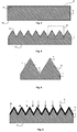
figures 3 et 4 , la gravure anisotrope de la face avant 1a du substrat 1 permet de structurer (ou texturer) la face avant 1a sous la forme de pyramides. Elle est, par exemple, réalisée en immergeant la face 1a du substrat 1 dans une solution aqueuse de gravure anisotrope, contenant de l'hydroxyde de potassium (KOH) et de l'alcool isopropylique (IPA), pendant 30 minutes et à une température de 80°C. De plus, lorsque seule la face avant 1a du substrat 1 est structurée comme représenté sur lesfigures 3 et 4 , la face arrière 1b peut être recouverte d'un masque de protection (par exemple en SiO2 ou Si3N4), résistant à la gravure anisotrope réalisée avec la solution aqueuse contenant KOH afin de préservée ladite face arrière 1b. - Pour un substrat en silicium présentant un axe cristallographique (100) orienté perpendiculairement à sa surface, les flancs «f» des pyramides obtenues forment, en général, un angle de 54,7° avec le plan « P » principal de la face 1a, c'est-à-dire le plan de la face 1a avant que celle-ci ne soit texturée. De plus, les largeurs des pyramides sont comprises entre 0,1µm et 40µm et avantageusement entre 1µm et 30µm, selon la concentration de la solution aqueuse et le temps de gravure.
- Comme illustré par l'agrandissement A d'une partie de la face avant 1a du substrat 1, l'état de surface de ladite face 1a après l'opération de gravure anisotrope et, en particulier, les flancs « f » des pyramides sont rugueux (schématisé par les traits en pointillés sur la
figure 5 ) et les sommets « s » des pyramides, tout comme les zones « b » disposées entre deux pyramides, sont abrupts (avec, en particulier, un rayon de courbure inférieur à 30nm). - Pour améliorer l'état de surface de la face 1a après l'opération de gravure anisotrope et, en particulier, pour lisser les flancs « f » des pyramides avantageusement créées et pour arrondir les zones dites « b » disposées entre deux pyramides et les sommets « s » desdites pyramides, il est proposé de réaliser un traitement par gravure isotrope comprenant au moins deux opérations successives consistant respectivement à former un film mince en oxyde de silicium d'une épaisseur contrôlée et à retirer ledit film mince ainsi formé, de préférence de manière homogène. L'épaisseur du film mince en oxyde de silicium est, de plus, comprise entre 2nm et 500nm et elle est, préférentiellement, homogène sur au moins les flancs « f » des pyramides et avantageusement sur toute la surface traitée.
- La formation d'un film mince en oxyde de silicium sur la face 1a du substrat 1 est réalisée par une opération d'oxydation par voie sèche activée thermiquement, c'est-à-dire en oxydant la face du substrat au moyen d'un agent oxydant non liquide tout en maintenant ladite face à une température supérieure à la température ambiante. L'agent oxydant peut, en particulier, être sous forme gazeuse ou bien être contenu dans un plasma. Il peut, par exemple, être de l'oxygène, de l'ozone, de l'eau, seuls ou en mélange. Plus particulièrement, l'activation thermique de l'oxydation par voie sèche consiste à fournir de l'énergie à la face du substrat, en appliquant un budget thermique défini par au moins une température supérieure à la température ambiante et avantageusement supérieure ou égale à 40°C. De plus, un tel budget thermique est, avantageusement, adapté pour permettre d'obtenir un compromis entre une montée en température rapide et suffisamment élevée pour générer le film mince en oxyde de silicium et l'obtention d'une température finale pas trop élevée pour éviter une altération des propriétés de surface ou de volume du substrat en silicium.
- En effet, le fait de former un film mince en oxyde de silicium d'une épaisseur particulière et contrôlée, puis de le retirer permet :
- de diminuer fortement la rugosité de surface de la face texturée du substrat et donc d'assurer un niveau minimum de densité d'état à l'interface avec la couche mince destinée à être directement disposée sur ladite face du substrat,
- et d'arrondir les angles des structures (sommets « s » et zones « b » des pyramides), ce qui permet d'obtenir une meilleure conformation des couches minces déposées ultérieurement.
- De plus, le traitement permet également d'éliminer une grande partie des contaminations particulaires, qui sont particulièrement critiques sur des substrats en silicium texturés.
- Plus particulièrement, le traitement par gravure isotrope peut être réalisé de différentes manières.
- En particulier, l'opération d'oxydation par voie sèche activée thermiquement peut être une oxydation thermique, c'est-à-dire une oxydation au moyen d'au moins un agent oxydant sous forme gazeuse ou contenu dans un plasma et par application à la face du substrat d'une température supérieure à la température ambiante et avantageusement supérieure ou égale à 40°C. En particulier, la température appliquée est inférieure à 1100°C. Une telle opération est, plus particulièrement, réalisée par un procédé de traitement rapide, également connu sous le nom anglo-saxon « Rapid Thermal Process » ou l'acronyme « RTP », afin d'obtenir une oxydation isotrope. Ainsi, l'opération d'oxydation par voie sèche est, de préférence, réalisée avec une montée en température très rapide (par exemple entre 100°C/s et 200°C/s). Par contre, la température finale obtenue à l'issue de cette montée en température est, de préférence, modérée afin d'éviter un endommagement de l'état de surface traité et des propriétés de volume du substrat.
- L'opération d'oxydation par voie sèche activée thermiquement peut aussi être assistée ou bien elle peut être obtenue par application de rayonnements ultraviolets de longueurs d'onde situées une gamme de 0,15µm à 0,4µm et avantageusement d'environ 254nm et d'environ 185nm. De même, elle peut, aussi, être assistée ou bien obtenue par un traitement par plasma, activé par exemple en radiofréquence, en micro-ondes ou en hyperfréquence. Le plasma peut, par exemple, être un plasma, tel qu'un plasma inductif ou un plasma de gravure réactive ionique (RIE). L'agent oxydant peut être un gaz ou un mélange de gaz pouvant contenir de l'oxygène, de l'ozone, de la vapeur d'eau ou bien il peut être une autre espèce gazeuse oxydante, seule ou en combinaison, sous une forme moléculaire, ionique, radicalaire ou atomique. La pression totale lors de l'opération d'oxydation peut être de tout type : elle peut être atmosphérique, sub-atmosphérique ou sur-atmosphérique. Il est aussi possible de faire varier la ou les pressions partielles de chaque espèce constituant l'agent oxydant en fonction de la pression totale. En particulier, la ou les pressions partielles de chaque espèce pourront être ajustées en fonction de la vitesse d'oxydation souhaitée.
- Selon un premier exemple, l'opération d'oxydation peut être une oxydation thermique réalisée avec une température de l'ordre de 400°C, avec un mélange gazeux d'oxygène et d'ozone (en particulier de 3 à 4% d'O3 par rapport à O2). Une telle opération permet d'obtenir un film mince en oxyde de silicium ayant une épaisseur suffisante pour améliorer l'état de surface, une fois ledit film retiré. On choisira, avantageusement, une épaisseur supérieure à 10 nm, qui peut être obtenue par exemple avec une température de 450°C pendant 3 heures. Des épaisseurs plus importantes peuvent être obtenues en augmentant la température et/ou le temps de traitement. Par exemple, on peut obtenir 25 nm d'oxyde de silicium avec une température de 550°C pendant 4 heures. On peut également, pour augmenter l'épaisseur d'oxyde de silicium généré pendant l'opération de traitement par gravure isotrope, réitérer un cycle opérationnel formé des opérations successives d'oxydation et de retrait, comme cela sera détaillé ultérieurement. L'épaisseur en oxyde de silicium est multipliée par quatre par rapport à un film obtenu par oxydation avec seulement de l'oxygène à la même température.
- Selon un second exemple, l'opération d'oxydation peut être une oxydation thermique réalisée entre 700°C et 800°C, assistée par rayonnement UV dans un mélange gazeux d'oxygène et d'ozone (environ 2ppm d'O3 par rapport à O2). Une telle opération permet d'obtenir un film mince en oxyde de silicium ayant une épaisseur suffisante pour améliorer l'état de surface, une fois ledit film retiré. L'épaisseur en oxyde de silicium est augmentée de 50% à 100% par rapport à un film obtenu par oxydation avec seulement de l'oxygène. L'épaisseur d'oxyde de silicium généré sera, avantageusement choisie de manière à être supérieure à 10 nm. Par exemple, avec une oxydation à 800°C pendant 140mn, on obtient un film d'oxyde de silicium d'une épaisseur de l'ordre de 25nm. Pour la même durée, on obtient un film de 60nm d'épaisseur, à 900°C et de 5nm à 700°C. L'épaisseur d'oxyde de silicium généré pendant l'opération de traitement par gravure isotrope peut aussi être augmentée par un cycle opérationnel formé des opérations successives d'oxydation et de retrait, comme cela sera détaillé ultérieurement.
- Selon un troisième exemple, l'opération d'oxydation peut être une oxydation obtenue par un traitement par plasma activé en micro-ondes (2,45GHz) et assisté par polarisation DC-magnétron (100V) et avec une pression partielle en oxygène d'environ 100mT. Dans ce cas, le film mince d'oxyde formé présente une épaisseur de l'ordre de 400nm pour une durée d'oxydation d'une heure, sur une surface d'une plaquette de silicium dont la température de surface est maintenue à environ 600°C.
- L'opération de retrait du film mince d'oxyde de silicium, suivant directement l'opération d'oxydation, peut être effectuée par voie sèche, par exemple par gravure ionique réactive (RIE) ou bien par voie humide, par exemple en immergeant la face 1a du substrat 1 dans une solution liquide contenant de l'acide chlorhydrique (HCI) et de l'acide fluorhydrique (HF) éventuellement tamponné (BHF). L'opération de retrait peut aussi être réalisée par traitement en milieu réducteur, par exemple en réalisant un traitement thermique sous hydrogène. Ces exemple d'étapes de retrait sont connues pour être des étapes de retrait homogène, c'est-à-dire un retrait avec une vitesse de retrait constante sur sous la surface, malgré la texturation.
- De plus, les deux opérations successives constituent un cycle opérationnel qui est répété au moins une fois. Une telle répétition est en particulier avantageuse lorsque le film mince en oxyde de silicium formé a une épaisseur de l'ordre de 2nm. La répétition des deux opérations successives d'oxydation et de retrait du film mince en oxyde de silicium permet d'optimiser le procédé et notamment d'obtenir un gain de temps.
- Par ailleurs, dans ce mode de réalisation, l'épaisseur globale (ou cumulée) d'oxyde de silicium formé au cours du traitement par gravure isotrope est avantageusement supérieure à 10nm et, de préférence, supérieure à 20nm. Par épaisseur globale d'oxyde de silicium, on entend dans ce mode de réalisation, la somme des épaisseurs des films minces en oxyde de silicium successivement formés au cours du traitement, ce qui correspond, plus précisément, à l'épaisseur d'un film d'oxyde de silicium formé par la totalité des différentes opérations successives d'oxydation dans l'hypothèse où elles ne seraient pas entrecoupées par des opérations de retrait.
- Dans un mode de réalisation ne faisant pas partie de l'invention, si le cycle opérationnel n'a pas besoin d'être répété, l'épaisseur du film mince d'oxyde de silicium formé pendant l'unique opération d'oxydation par voie sèche activée thermiquement du traitement est, aussi, de manière avantageuse, supérieure à 10nm et, de préférence, supérieure à 20nm. On parlera, par analogie, aussi dans ce cas, d'épaisseur globale d'oxyde de silicium formé pendant le traitement par gravure isotrope.
- La réalisation d'un ou plusieurs cycles opérationnel entraîne une très faible gravure du silicium, en lissant les flancs des pyramides et en modifiant non seulement la géométrie des sommets des pyramides mais aussi celle des zones disposées entre les pyramides, tout en maintenant le confinement optique de la texturation à un très bon niveau.
- Le traitement par gravure isotrope de la face 1a du substrat 1 est, par exemple, illustré sur les
figures 6 à 8 . Les flèches F sur lafigure 6 représentent l'opération d'oxydation par voie sèche activée thermiquement formant le film mince 11 en oxyde de silicium, sur la face 1a du substrat 1 et permettant l'arrondissement des sommets « s » des pyramides et des zones en creux « b » disposées entre les pyramides. Une fois l'opération réalisée, le film mince en oxyde de silicium 11 est retiré (figure 7 ). L'agrandissement A' représenté sur lafigure 8 illustre un tel arrondissement pour les sommets « s » des pyramides et les zones en creux « b » disposées entre les pyramides ainsi que le lissage des flancs « f » (traits pleins sur lafigure 8 ), une fois le film mince 11 retiré. - Puis, comme illustré sur la
figure 9 , l'opération de gravure isotrope peut être suivie de la formation, sur ladite surface, d'un empilement multicouche comprenant successivement : - une couche mince en silicium amorphe intrinsèque 2 constituant, sur la
figure 9 , une couche de passivation, - une couche mince en silicium amorphe 3 présentant un type de dopage opposé au type de dopage du substrat en silicium cristallin,
- une électrode 4
- et un collecteur de courant 5.
- De plus, la face avant 1a du substrat 1 en silicium cristallin peut subir, après le traitement par gravure isotrope et avant la formation de l'empilement multicouche, au moins une étape de nettoyage et une étape de séchage. Ainsi, à titre d'exemple, la face 1a du substrat 1 peut subir un traitement avec un mélange d'acide fluorhydrique et d'acide chlorhydrique (HF/HCl), avec une faible teneur en HF, afin d'éviter une nouvelle contamination de la surface. Le traitement de nettoyage peut aussi être réalisé avec des vapeurs d'acide fluorhydrique (HF), suivi d'un rinçage avec un mélange d'eau désaérée sans oxygène libre et d'HCI pour éviter toute pollution de la surface par de l'oxygène. Cette pollution entraînerait la formation prématurée d'un oxyde natif, néfaste pour la réalisation de bonnes passivations de surface. De plus, une opération de séchage peut suivre, pour éviter tout dépôt contaminant sur les pyramides. Elle est, par exemple, réalisée avec de l'alcool isopropylique (IPA) vaporisé ou dans un liquide à faible tension de surface ou bien par immersion dans une solution liquide telle que de l'eau désaérée suivie d'une immersion dans une solution d'IPA de préférence chauffée. Avantageusement, la formation de l'empilement multicouche, par exemple par dépôt chimique en phase vapeur assisté par plasma (PECVD) peut alors être réalisée jusqu'à une demi-heure après le séchage, sans diminution du rendement des cellules photovoltaïques obtenues.
- Comme dans les modes de réalisation représentés sur les
figures 1 et 2 , la face arrière 1b du substrat 1 peut, avantageusement, être recouverte par au moins une couche mince. Elle peut, par exemple, être recouverte par une électrode 6 telle que celle représentée sur lafigure 1 ou bien par un empilement multicouche tel que celui représenté sur lafigure 2 . - De plus, l'invention n'est pas limitée aux modes de réalisation décrits ci-dessus, en particulier en ce qui concerne le type de dopage du substrat 1 et des couches en silicium amorphe 3 et 8. Par conséquent, l'invention n'est pas limitée aux modes de réalisation comprenant un substrat en silicium cristallin dopé n et des couches en silicium amorphe 3 et 8, respectivement dopées p et n. La couche en silicium amorphe 3 présente un type de dopage contraire à celui du substrat 1, afin de former l'hétérojonction de la cellule photovoltaïque et la couche en silicium amorphe 8 disposée du côté de la face arrière 1b du substrat 1 présente, en particulier, un type de dopage identique à celui du substrat 1. Par ailleurs, au lieu d'être en silicium amorphe, les couches minces 3 et 8 peuvent aussi être en silicium microcristallin.
- De même, les modes de réalisation décrits ci-dessus illustrent une gravure anisotrope et un traitement par gravure isotrope de la face avant 1a du substrat 1. Cependant, ces gravures pourraient être envisagées non pas sur la face avant 1a du substrat 1, mais sur sa face arrière 1b ou même, en plus de la face avant 1a du substrat 1, sur la face arrière 1b du substrat 1. Dans ce cas, la couche mince en silicium amorphe ou microcristallin 8 de l'empilement multicouche disposé sur la face arrière 1b présente un type de dopage identique à celui du substrat en silicium cristallin 1.
- Par ailleurs, selon une variante de réalisation, une étape de dépôt d'une couche d'un matériau d'une nature et/ou d'une structure cristalline et/ou d'une morphologie différente à celle du substrat 1 peut être réalisée entre l'étape de gravure anisotrope et le traitement par gravure isotrope. Une telle couche peut être formée par du silicium amorphe ou du silicium polycristallin ou bien par de l'oxyde de silicium ou par un oxyde à haute permittivité (High K) tel que l'HfO2 ou Al2O3 ou ZrO2. Elle peut, par exemple, être déposée par une technique de dépôt chimique en phase vapeur (CVD), à une température appropriée (par exemple de l'ordre de 100°C à 800°C).
- Ainsi, à titre d'exemple, sur les
figures 10 à 12 , une couche 12a formée par du silicium amorphe ou polycristallin est disposée sur la face avant 1a du substrat 1 entre l'étape de gravure anisotrope et le traitement par gravure isotrope. Dans ce cas, l'opération d'oxydation par voie sèche activée thermiquement permet d'oxyder le silicium de la couche 12a en même temps que la face du substrat 1a sur laquelle est disposée ladite couche 12, afin de former un film mince en oxyde de silicium 11. - Sur les
figures 13 à 15 , une couche 12b formée par de l'oxyde de silicium est disposée sur la face avant 1a du substrat 1, une fois ladite face texturée. Dans ce cas, l'opération d'oxydation par voie sèche activée thermiquement permet d'oxyder, au travers de la couche 12b, la face avant du substrat 1, afin de former entre le substrat 1 et la couche 12b, un film mince en oxyde de silicium 11. - Dans tous les cas et comme illustré sur les
figures 12 et15 , la couche 12a ou 12b est retirée lors de l'opération de retrait du film mince 11 en oxyde de silicium. De plus, cette couche 12a ou 12b doit être suffisamment épaisse, par exemple de l'ordre de la centaine de nanomètres. Elle est destinée à favoriser l'amélioration de l'état de surface de la surface traitée par gravure isotrope. En particulier, il se forme lors du dépôt de cette couche, un arrondissement au sommet « s » des pyramides et dans les zones « b » entre les pyramides. Ainsi, il est possible de différencier l'oxydation des flancs « f » de l'oxydation des zones « b » et des sommets « s » par rapport aux flancs « f » des pyramides, ce qui améliore le lissage des flancs « f » et l'arrondissement des zones « b » et des sommets « s ». - À titre d'exemple, un substrat présentant initialement un axe cristallographique <100> orienté perpendiculairement à sa surface est texturé afin de présenter, en surface, des pyramides ayant des sommets « s » et des creux « b » entre les pyramides ayant chacun une courbure présentant typiquement un rayon moyen de 30 nm. Il peut s'agir d'un substrat. Une couche 12a en silicium, d'une épaisseur de l'ordre de 100 nm est déposée par LPCVD sur ladite surface, dans une gamme de température de 500 à 620°C. Le silicium ainsi déposé est, alors, amorphe ou polycristallin. De plus, suivant le besoin, cette couche 12a peut être dopée. Il est à noter qu'après le dépôt de la couche 12a, les sommets « s » et les creux « b » formés par la couche 12a sont arrondies. Cet arrondissement permet d'obtenir un rayon de courbure de l'ordre de 200nm de rayon de courbure à l'aplomb des creux des pyramides. De plus, il est possible d'ajuster l'épaisseur de la couche 12a en fonction du rayon de courbure souhaité, selon les besoins de l'utilisateur. Cette couche est alors oxydée thermiquement pour en consommer toute son épaisseur par exemple par oxydation à 950°C sous vapeur d'eau (mode « steam »). Lors de l'oxydation, la présence de l'arrondi à la surface de la couche 12a en silicium induit alors un arrondi à la surface du substrat en silicium initial, au niveau des sommets et des creux des pyramides avec un rayon de courbure de l'ordre de 200 à 300 nm à l'aplomb des creux entre les pyramides. Après le retrait de l'oxyde, cette forme arrondie est conservée.
- Selon une autre variante de réalisation, la couche de passivation formée par la couche mince en silicium amorphe intrinsèque 2 sur la
figure 9 peut être au moins formée par une couche mince en oxyde cristallin de silicium disposée directement sur la surface du substrat préalablement traitée par gravure isotrope. Une telle couche mince en oxyde cristallin de silicium est, avantageusement, obtenue par oxydation superficielle radicalaire de la surface du substrat (1), par exemple au moyen de radicaux oxygénés obtenu à partir d'oxygène et/ou d'ozone et/ou d'eau. et elle n'est pas retirée. Elle a, avantageusement, une épaisseur inférieure ou égale à 2nm et elle peut être recouverte par de l'oxyde amorphe de silicium. À titre d'exemple, l'oxydation d'une partie superficielle du substrat 1 peut être réalisée à partir d'oxygène et de rayonnements ultraviolets ayant une gamme de longueurs d'onde comprise entre 160nm et 400nm. Les longueurs d'onde des rayonnements ultraviolets utilisés sont, par exemple, d'environ 185nm et d'environ 254nm. Dans ce mode particulier de réalisation, l'oxygène, sous l'action des rayonnements ultraviolets, se dissocie en radicaux libres O· et en ozone et lesdits radicaux libres oxydent la surface du silicium et forment au moins la couche mince en oxyde cristallin de silicium. - De plus, dans une autre variante de réalisation, la couche de passivation peut être formée par la couche mince en oxyde cristallin de silicium et par la couche mince en silicium amorphe intrinsèque, cette dernière étant disposée entre la couche mince en oxyde cristallin de silicium et la couche mince en silicium amorphe ou microcristallin.
- Enfin les modes de réalisation décrits ci-dessus concernent une cellule photovoltaïque à hétérojonction. Cependant, le traitement par gravure isotrope exposé dans ces différents modes de réalisation peut être appliqué à une surface d'un substrat en silicium cristallin ayant préalablement subi une étape de gravure anisotrope pour réaliser tout type de cellules photovoltaïques et plus particulièrement pour réaliser des cellules photovoltaïques à homojonction.
Claims (14)
- Procédé de réalisation d'au moins une cellule photovoltaïque comprenant les étapes successives suivantes :- gravure anisotrope d'une surface (1a, 1b) d'un substrat (1) en silicium cristallin configurée pour structurer la face avant (1a) sous la forme de pyramides ;- et traitement par gravure isotrope de ladite surface (1a, 1b), ledit traitement comprenant la formation d'un oxyde de silicium et le retrait dudit oxyde de silicium ;caractérisé en ce que le traitement par gravure isotrope de ladite surface (1) comprend deux opérations successives, respectivement constituées par une oxydation par voie sèche activée thermiquement formant, à ladite surface (1a, 1b) du substrat (1), un film mince (11) d'oxyde de silicium d'une épaisseur comprise entre 2nm et 500nm et par le retrait dudit film mince (11) en oxyde de silicium ;
et en ce que les deux opérations successives constituent un cycle opérationnel répété au moins une fois pendant le traitement par gravure isotrope, de sorte à arrondir les sommets (s) des pyramides et les zones (b) disposées entre deux pyramides. - Procédé selon la revendication 1, caractérisé en ce que l'opération d'oxydation par voie sèche activée thermiquement comprend l'application à ladite surface (1a, 1b) du substrat (1) d'une température supérieure à la température ambiante et l'utilisation d'un agent oxydant sous une forme gazeuse ou contenu dans un plasma.
- Procédé selon la revendication 2, caractérisé en ce que l'opération d'oxydation par voie sèche activée thermiquement comprend l'application d'un rayonnement ultraviolet sur ladite surface (1a, 1b) du substrat (1).
- Procédé selon la revendication 2, caractérisé en ce que l'opération d'oxydation par voie sèche activée thermiquement comprend un traitement par plasma activé en micro-ondes, en radiofréquence ou en hyperfréquence.
- Procédé selon l'une quelconque des revendications 1 à 4, caractérisé en ce que l'opération de retrait dudit film mince (11) en oxyde de silicium est effectuée par voie sèche.
- Procédé selon l'une quelconque des revendications 1 à 4, caractérisé en ce que l'opération de retrait dudit film mince (11) en oxyde de silicium est effectuée par voie humide.
- Procédé selon l'une quelconque des revendications 1 à 4, caractérisé en ce que l'opération de retrait dudit film mince (11) en oxyde de silicium est effectuée par traitement en milieu réducteur.
- Procédé selon l'une quelconque des revendications 1 à 7, caractérisé en ce que l'oxyde de silicium formé au cours du traitement par gravure isotrope présente une épaisseur globale comprise entre 10nm et 500nm.
- Procédé selon l'une quelconque des revendications 1 à 8, caractérisé en ce que la surface (1a, 1b) du substrat (1), une fois celle-ci traitée par gravure isotrope est recouverte au moins en partie d'un empilement multicouche comprenant successivement :- une couche de passivation (2),- une couche mince en silicium amorphe ou microcristallin (3, 8) présentant un type de dopage prédéterminé,- une électrode (4)- et un collecteur de courant (5).
- Procédé selon la revendication 9, caractérisé en ce que le type de dopage de la couche mince en silicium amorphe ou microcristallin (3) est opoosé au type de dopage du substrat en silicium cristallin (1).
- Procédé selon la revendication 9, caractérisé en ce que le type de dopage de la couche mince en silicium amorphe ou microcristallin (8) est identique au type de dopage du substrat en silicium cristallin (1).
- Procédé selon l'une quelconque des revendications 9 à 11, caractérisé en ce qu'il comporte une étape de dépôt d'une couche (12a, 12b) formée avec un matériau d'une nature et/ou d'une structure cristalline et/ou d'une morphologie différente de celle du substrat (1), ladite étape étant réalisée entre la gravure anisotrope de la surface (1a, 1b) et le traitement par gravure isotrope et en ce que ladite couche est retirée pendant l'opération de retrait du film mince (11) d'oxyde de silicium.
- Procédé selon l'une quelconque des revendications 9 à 12, caractérisé en ce que la couche de passivation (2) est formée par au moins une couche mince en silicium amorphe intrinsèque (2).
- Procédé selon l'une quelconque des revendications 9 à 13, caractérisée en ce que la couche de passivation (2) est formée par au moins une couche mince en oxyde cristallin de silicium en contact direct avec ladite surface (1a, 1b) du substrat (1).
Applications Claiming Priority (2)
| Application Number | Priority Date | Filing Date | Title |
|---|---|---|---|
| FR1000306A FR2955707B1 (fr) | 2010-01-27 | 2010-01-27 | Procede de realisation d'une cellule photovoltaique avec preparation de surface d'un substrat en silicium cristallin |
| PCT/FR2011/000049 WO2011092401A2 (fr) | 2010-01-27 | 2011-01-26 | Procede de realisation d'une cellule photovoltaique avec preparation de surface d'un substrat en silicium cristallin |
Publications (2)
| Publication Number | Publication Date |
|---|---|
| EP2529418A2 EP2529418A2 (fr) | 2012-12-05 |
| EP2529418B1 true EP2529418B1 (fr) | 2019-06-26 |
Family
ID=43333000
Family Applications (1)
| Application Number | Title | Priority Date | Filing Date |
|---|---|---|---|
| EP11708520.9A Active EP2529418B1 (fr) | 2010-01-27 | 2011-01-26 | Procede de realisation d'une cellule photovoltaique avec preparation de surface d'un substrat en silicium cristallin |
Country Status (7)
| Country | Link |
|---|---|
| US (1) | US8877539B2 (fr) |
| EP (1) | EP2529418B1 (fr) |
| JP (1) | JP6033687B2 (fr) |
| KR (1) | KR20120104441A (fr) |
| CN (1) | CN102725869B (fr) |
| FR (1) | FR2955707B1 (fr) |
| WO (1) | WO2011092401A2 (fr) |
Families Citing this family (26)
| Publication number | Priority date | Publication date | Assignee | Title |
|---|---|---|---|---|
| DE102008048540A1 (de) * | 2008-09-15 | 2010-04-15 | Gebr. Schmid Gmbh & Co. | Verfahren zur Behandlung von Substraten, Substrat und Behandlungseinrichtung zur Durchführung des Verfahrens |
| US20130247967A1 (en) * | 2012-03-23 | 2013-09-26 | Scott Harrington | Gaseous ozone (o3) treatment for solar cell fabrication |
| WO2014064929A1 (fr) * | 2012-10-23 | 2014-05-01 | 三洋電機株式会社 | Cellule solaire |
| TWI568003B (zh) * | 2012-12-19 | 2017-01-21 | 茂迪股份有限公司 | 太陽能電池及其製造方法與太陽能電池模組 |
| US9082925B2 (en) | 2013-03-13 | 2015-07-14 | Sunpower Corporation | Methods for wet chemistry polishing for improved low viscosity printing in solar cell fabrication |
| JP5945066B2 (ja) * | 2013-03-19 | 2016-07-05 | 長州産業株式会社 | 光起電力素子の製造方法 |
| EP2980861B1 (fr) * | 2013-03-28 | 2020-01-08 | Panasonic Intellectual Property Management Co., Ltd. | Cellule solaire |
| JP6114630B2 (ja) * | 2013-05-27 | 2017-04-12 | 株式会社カネカ | 結晶シリコン系太陽電池の製造方法 |
| FR3015770B1 (fr) | 2013-12-19 | 2016-01-22 | Commissariat Energie Atomique | Procede et systeme de controle de qualite de cellules photovoltaiques |
| WO2015152244A1 (fr) * | 2014-04-02 | 2015-10-08 | 三菱電機株式会社 | Élément de capteur, procédé de fabrication d'un élément de capteur, dispositif de détection, et procédé de fabrication d'un dispositif de détection |
| CN104143590B (zh) * | 2014-08-08 | 2017-08-25 | 中国科学院宁波材料技术与工程研究所 | 一种简单快速的硅表面钝化方法 |
| US9837259B2 (en) | 2014-08-29 | 2017-12-05 | Sunpower Corporation | Sequential etching treatment for solar cell fabrication |
| CN107078179B (zh) * | 2014-09-30 | 2019-04-26 | 株式会社钟化 | 晶体硅太阳能电池的制造方法、及太阳能电池模块的制造方法 |
| JP6513788B2 (ja) * | 2015-03-24 | 2019-05-15 | 株式会社カネカ | 結晶シリコン系太陽電池の製造方法および結晶シリコン系太陽電池モジュールの製造方法 |
| CN106328736B (zh) * | 2015-06-16 | 2018-05-04 | 镇江大全太阳能有限公司 | 一种抗lid黑硅太阳能高效电池及其生产方法 |
| WO2017051635A1 (fr) * | 2015-09-24 | 2017-03-30 | シャープ株式会社 | Substrat semi-conducteur, élément de conversion photoélectrique, procédé de fabrication de substrat semi-conducteur et procédé de fabrication d'élément de conversion photoélectrique |
| DE102015015017A1 (de) * | 2015-11-19 | 2017-05-24 | Institut Für Solarenergieforschung Gmbh | Solarzelle und Verfahren zur Herstellung einer Solarzelle mit mehreren durch ladungsträgerselektive Kontakte miteinander verbundenen Absorbern |
| CN107403849A (zh) * | 2016-05-20 | 2017-11-28 | 昱晶能源科技股份有限公司 | 太阳能电池及制造太阳能电池的方法 |
| CN105895714A (zh) * | 2016-06-22 | 2016-08-24 | 苏州协鑫集成科技工业应用研究院有限公司 | 平滑修饰液及平滑修饰方法及异质结太阳能电池硅片及异质结太阳能电池 |
| CN106098815A (zh) * | 2016-07-01 | 2016-11-09 | 李玉强 | 光伏太阳能晶硅锥针式电池毯 |
| CN106571411B (zh) * | 2016-10-19 | 2018-09-21 | 苏州阿特斯阳光电力科技有限公司 | 一种晶体硅片的刻蚀方法 |
| KR20180119969A (ko) | 2017-04-26 | 2018-11-05 | 엘지전자 주식회사 | 태양 전지 및 이의 제조 방법 |
| KR102541379B1 (ko) | 2017-05-29 | 2023-06-08 | 상라오 징코 솔라 테크놀러지 디벨롭먼트 컴퍼니, 리미티드 | 페로브스카이트 실리콘 탠덤 태양전지 및 제조 방법 |
| KR102584087B1 (ko) * | 2018-03-19 | 2023-10-04 | 상라오 징코 솔라 테크놀러지 디벨롭먼트 컴퍼니, 리미티드 | 텐덤 태양전지의 제조 방법 |
| CN114975650A (zh) * | 2022-03-16 | 2022-08-30 | 江苏日托光伏科技股份有限公司 | 一种单晶硅金字塔及其制备方法 |
| CN116435403B (zh) * | 2023-02-28 | 2024-09-17 | 六智韬新能源科技(上海)有限公司 | 一种柔性单晶硅片和柔性太阳电池及其制备方法 |
Citations (4)
| Publication number | Priority date | Publication date | Assignee | Title |
|---|---|---|---|---|
| JPH0621214A (ja) * | 1992-07-03 | 1994-01-28 | Seiko Epson Corp | 半導体装置の製造方法 |
| US6624049B1 (en) * | 1996-07-08 | 2003-09-23 | Semiconductor Energy Laboratory Co., Ltd. | Semiconductor device and method of manufacturing the same |
| WO2009094578A2 (fr) * | 2008-01-24 | 2009-07-30 | Applied Materials, Inc. | Structure de pile solaire hit améliorée |
| US20090215218A1 (en) * | 2008-02-25 | 2009-08-27 | Suniva, Inc. | Method for making solar cell having crystalline silicon p-n homojunction and amorphous silicon heterojunctions for surface passivation |
Family Cites Families (26)
| Publication number | Priority date | Publication date | Assignee | Title |
|---|---|---|---|---|
| US4818337A (en) * | 1986-04-11 | 1989-04-04 | University Of Delaware | Thin active-layer solar cell with multiple internal reflections |
| JPH0738111A (ja) * | 1993-07-22 | 1995-02-07 | Fujitsu Ltd | 薄膜トランジスタの形成方法 |
| JPH0766437A (ja) * | 1993-08-30 | 1995-03-10 | Tonen Corp | 光電変換装置用基板の製造方法 |
| JPH0786271A (ja) | 1993-09-17 | 1995-03-31 | Fujitsu Ltd | シリコン酸化膜の作製方法 |
| US5871653A (en) * | 1996-10-30 | 1999-02-16 | Advanced Materials Engineering Research, Inc. | Methods of manufacturing micro-lens array substrates for implementation in flat panel display |
| US6320238B1 (en) * | 1996-12-23 | 2001-11-20 | Agere Systems Guardian Corp. | Gate structure for integrated circuit fabrication |
| JP3271990B2 (ja) * | 1997-03-21 | 2002-04-08 | 三洋電機株式会社 | 光起電力素子及びその製造方法 |
| JP3233281B2 (ja) | 1999-02-15 | 2001-11-26 | 日本電気株式会社 | ゲート酸化膜の形成方法 |
| US6890450B2 (en) | 2001-02-02 | 2005-05-10 | Intel Corporation | Method of providing optical quality silicon surface |
| US6916717B2 (en) * | 2002-05-03 | 2005-07-12 | Motorola, Inc. | Method for growing a monocrystalline oxide layer and for fabricating a semiconductor device on a monocrystalline substrate |
| JP2004152851A (ja) * | 2002-10-29 | 2004-05-27 | Oki Electric Ind Co Ltd | 半導体装置の製造方法 |
| JP2004172271A (ja) * | 2002-11-19 | 2004-06-17 | Mitsubishi Electric Corp | 太陽電池の製造方法及び太陽電池 |
| US7402448B2 (en) * | 2003-01-31 | 2008-07-22 | Bp Corporation North America Inc. | Photovoltaic cell and production thereof |
| JP4682508B2 (ja) * | 2003-11-14 | 2011-05-11 | 信越半導体株式会社 | シリコンエピタキシャルウェーハの製造方法 |
| JP2005175023A (ja) | 2003-12-08 | 2005-06-30 | National Institute Of Advanced Industrial & Technology | 高密度シリコン酸化膜、その製造方法およびそれを用いた半導体デバイス |
| JP2007194485A (ja) * | 2006-01-20 | 2007-08-02 | Osaka Univ | 太陽電池用シリコン基板の製造方法 |
| EP1850378A3 (fr) | 2006-04-28 | 2013-08-07 | Semiconductor Energy Laboratory Co., Ltd. | Dispositif à mémoire et dispositif à semi-conducteur |
| US7737357B2 (en) | 2006-05-04 | 2010-06-15 | Sunpower Corporation | Solar cell having doped semiconductor heterojunction contacts |
| JP5019397B2 (ja) * | 2006-12-01 | 2012-09-05 | シャープ株式会社 | 太陽電池およびその製造方法 |
| JP2008300440A (ja) * | 2007-05-29 | 2008-12-11 | Sanyo Electric Co Ltd | 太陽電池セル及び太陽電池モジュール |
| CN101102545B (zh) | 2007-07-24 | 2010-08-18 | 中兴通讯股份有限公司 | 移动多媒体广播业务指南生成及发送的系统与方法 |
| WO2009067475A1 (fr) * | 2007-11-19 | 2009-05-28 | Applied Materials, Inc. | Procédés de métallisation de pile solaire cristalline |
| CN102017176A (zh) * | 2008-03-25 | 2011-04-13 | 应用材料股份有限公司 | 结晶太阳能电池的表面清洁与纹理化工艺 |
| DE102008056455B3 (de) * | 2008-11-07 | 2010-04-29 | Centrotherm Photovoltaics Technology Gmbh | Oxidations- und Reinigungsverfahren für Siliziumscheiben |
| JP5537101B2 (ja) * | 2009-09-10 | 2014-07-02 | 株式会社カネカ | 結晶シリコン系太陽電池 |
| US20120083127A1 (en) * | 2010-09-30 | 2012-04-05 | Tokyo Electron Limited | Method for forming a pattern and a semiconductor device manufacturing method |
-
2010
- 2010-01-27 FR FR1000306A patent/FR2955707B1/fr not_active Expired - Fee Related
-
2011
- 2011-01-26 CN CN201180007626.XA patent/CN102725869B/zh not_active Expired - Fee Related
- 2011-01-26 JP JP2012550487A patent/JP6033687B2/ja not_active Expired - Fee Related
- 2011-01-26 KR KR1020127022312A patent/KR20120104441A/ko not_active Abandoned
- 2011-01-26 WO PCT/FR2011/000049 patent/WO2011092401A2/fr not_active Ceased
- 2011-01-26 EP EP11708520.9A patent/EP2529418B1/fr active Active
- 2011-01-26 US US13/522,829 patent/US8877539B2/en not_active Expired - Fee Related
Patent Citations (4)
| Publication number | Priority date | Publication date | Assignee | Title |
|---|---|---|---|---|
| JPH0621214A (ja) * | 1992-07-03 | 1994-01-28 | Seiko Epson Corp | 半導体装置の製造方法 |
| US6624049B1 (en) * | 1996-07-08 | 2003-09-23 | Semiconductor Energy Laboratory Co., Ltd. | Semiconductor device and method of manufacturing the same |
| WO2009094578A2 (fr) * | 2008-01-24 | 2009-07-30 | Applied Materials, Inc. | Structure de pile solaire hit améliorée |
| US20090215218A1 (en) * | 2008-02-25 | 2009-08-27 | Suniva, Inc. | Method for making solar cell having crystalline silicon p-n homojunction and amorphous silicon heterojunctions for surface passivation |
Also Published As
| Publication number | Publication date |
|---|---|
| FR2955707A1 (fr) | 2011-07-29 |
| US8877539B2 (en) | 2014-11-04 |
| WO2011092401A2 (fr) | 2011-08-04 |
| US20120288985A1 (en) | 2012-11-15 |
| CN102725869A (zh) | 2012-10-10 |
| CN102725869B (zh) | 2016-07-20 |
| KR20120104441A (ko) | 2012-09-20 |
| JP6033687B2 (ja) | 2016-11-30 |
| JP2013518425A (ja) | 2013-05-20 |
| WO2011092401A3 (fr) | 2011-11-17 |
| EP2529418A2 (fr) | 2012-12-05 |
| FR2955707B1 (fr) | 2012-03-23 |
Similar Documents
| Publication | Publication Date | Title |
|---|---|---|
| EP2529418B1 (fr) | Procede de realisation d'une cellule photovoltaique avec preparation de surface d'un substrat en silicium cristallin | |
| EP2529416B1 (fr) | Cellule photovoltaïque comprenant un film mince de passivation en oxyde cristallin de silicium et procédé de réalisation | |
| EP2471103B1 (fr) | Procédé de texturation de la surface d'un substrat de silicium et substrat de silicium texturé pour cellule solaire | |
| WO2008062685A1 (fr) | Substrat accompagné de film conducteur transparent pour dispositif de conversion photoélectrique, procédé de fabrication du substrat et dispositif de conversion photoélectrique l'utilisant | |
| WO2016052635A1 (fr) | Procédé de fabrication de cellule solaire à base de silicium cristallin et procédé de fabrication de module de cellules solaires | |
| EP3291283B1 (fr) | Surface d'emission de rayonnement infrarouge ir a emissivite thermique elevee et a grande duree de vie et son procede de fabrication | |
| EP2159851A1 (fr) | Procédé pour limiter la croissance épitaxiale dans un dispositif photoélectrique à hétérojonctions et un tel dispositif photoélctrique | |
| EP2491576B1 (fr) | Procede de fabrication d'un film multicouche comprenant au moins une couche mince de silicium cristallin | |
| EP1913642A1 (fr) | Revetement anti-reflet, en particulier pour cellules solaires, et procede de fabrication de ce revetement | |
| EP2801113B1 (fr) | Procédé de production à basse température de nanostructures semi-conductrices à jonction radiale, dispositif a jonction radiale et cellule solaire comprenant des nanostructures à jonction radiale | |
| WO2019053368A1 (fr) | Procede de fabrication d'une cellule photovoltaïque a homojonction | |
| WO2014029836A2 (fr) | Procede de realisation de contacts electriques d'un dispositif semi-conducteur | |
| EP1735843B1 (fr) | Procede de fabrication de plaques de silicium polycristallin | |
| FR2955706A1 (fr) | Procede de realisation d'une cellule photovoltaique avec gravure isotrope d'un substrat en silicium cristallin au moyen d'ozone et d'acide fluorhydrique | |
| EP2795677B1 (fr) | Procede de texturation de la surface d'un substrat de silicium, substrat structure et dispositif photovoltaïque comportant un tel substrat structure | |
| WO2018104650A1 (fr) | Procédé de fabrication d'un dispositif à semi-conducteur et dispositif à semi-conducteur | |
| RU2600076C1 (ru) | Способ получения светопоглощающей кремниевой структуры |
Legal Events
| Date | Code | Title | Description |
|---|---|---|---|
| PUAI | Public reference made under article 153(3) epc to a published international application that has entered the european phase |
Free format text: ORIGINAL CODE: 0009012 |
|
| 17P | Request for examination filed |
Effective date: 20120724 |
|
| AK | Designated contracting states |
Kind code of ref document: A2 Designated state(s): AL AT BE BG CH CY CZ DE DK EE ES FI FR GB GR HR HU IE IS IT LI LT LU LV MC MK MT NL NO PL PT RO RS SE SI SK SM TR |
|
| DAX | Request for extension of the european patent (deleted) | ||
| RIC1 | Information provided on ipc code assigned before grant |
Ipc: H01L 31/20 20060101AFI20130429BHEP Ipc: H01L 31/075 20120101ALN20130429BHEP Ipc: H01L 21/306 20060101ALI20130429BHEP Ipc: H01L 31/0236 20060101ALI20130429BHEP |
|
| 17Q | First examination report despatched |
Effective date: 20151210 |
|
| GRAP | Despatch of communication of intention to grant a patent |
Free format text: ORIGINAL CODE: EPIDOSNIGR1 |
|
| STAA | Information on the status of an ep patent application or granted ep patent |
Free format text: STATUS: GRANT OF PATENT IS INTENDED |
|
| INTG | Intention to grant announced |
Effective date: 20190131 |
|
| RIN1 | Information on inventor provided before grant (corrected) |
Inventor name: MORICEAU, HUBERT Inventor name: MUR, PIERRE Inventor name: RIBEYRON, PIERRE-JEAN |
|
| GRAS | Grant fee paid |
Free format text: ORIGINAL CODE: EPIDOSNIGR3 |
|
| GRAA | (expected) grant |
Free format text: ORIGINAL CODE: 0009210 |
|
| STAA | Information on the status of an ep patent application or granted ep patent |
Free format text: STATUS: THE PATENT HAS BEEN GRANTED |
|
| AK | Designated contracting states |
Kind code of ref document: B1 Designated state(s): AL AT BE BG CH CY CZ DE DK EE ES FI FR GB GR HR HU IE IS IT LI LT LU LV MC MK MT NL NO PL PT RO RS SE SI SK SM TR |
|
| REG | Reference to a national code |
Ref country code: GB Ref legal event code: FG4D Free format text: NOT ENGLISH |
|
| REG | Reference to a national code |
Ref country code: CH Ref legal event code: EP |
|
| REG | Reference to a national code |
Ref country code: DE Ref legal event code: R096 Ref document number: 602011059993 Country of ref document: DE |
|
| REG | Reference to a national code |
Ref country code: AT Ref legal event code: REF Ref document number: 1149310 Country of ref document: AT Kind code of ref document: T Effective date: 20190715 |
|
| REG | Reference to a national code |
Ref country code: IE Ref legal event code: FG4D Free format text: LANGUAGE OF EP DOCUMENT: FRENCH |
|
| REG | Reference to a national code |
Ref country code: NL Ref legal event code: MP Effective date: 20190626 |
|
| PG25 | Lapsed in a contracting state [announced via postgrant information from national office to epo] |
Ref country code: AL Free format text: LAPSE BECAUSE OF FAILURE TO SUBMIT A TRANSLATION OF THE DESCRIPTION OR TO PAY THE FEE WITHIN THE PRESCRIBED TIME-LIMIT Effective date: 20190626 Ref country code: NO Free format text: LAPSE BECAUSE OF FAILURE TO SUBMIT A TRANSLATION OF THE DESCRIPTION OR TO PAY THE FEE WITHIN THE PRESCRIBED TIME-LIMIT Effective date: 20190926 Ref country code: LT Free format text: LAPSE BECAUSE OF FAILURE TO SUBMIT A TRANSLATION OF THE DESCRIPTION OR TO PAY THE FEE WITHIN THE PRESCRIBED TIME-LIMIT Effective date: 20190626 Ref country code: FI Free format text: LAPSE BECAUSE OF FAILURE TO SUBMIT A TRANSLATION OF THE DESCRIPTION OR TO PAY THE FEE WITHIN THE PRESCRIBED TIME-LIMIT Effective date: 20190626 Ref country code: SE Free format text: LAPSE BECAUSE OF FAILURE TO SUBMIT A TRANSLATION OF THE DESCRIPTION OR TO PAY THE FEE WITHIN THE PRESCRIBED TIME-LIMIT Effective date: 20190626 Ref country code: HR Free format text: LAPSE BECAUSE OF FAILURE TO SUBMIT A TRANSLATION OF THE DESCRIPTION OR TO PAY THE FEE WITHIN THE PRESCRIBED TIME-LIMIT Effective date: 20190626 |
|
| REG | Reference to a national code |
Ref country code: LT Ref legal event code: MG4D |
|
| PG25 | Lapsed in a contracting state [announced via postgrant information from national office to epo] |
Ref country code: RS Free format text: LAPSE BECAUSE OF FAILURE TO SUBMIT A TRANSLATION OF THE DESCRIPTION OR TO PAY THE FEE WITHIN THE PRESCRIBED TIME-LIMIT Effective date: 20190626 Ref country code: LV Free format text: LAPSE BECAUSE OF FAILURE TO SUBMIT A TRANSLATION OF THE DESCRIPTION OR TO PAY THE FEE WITHIN THE PRESCRIBED TIME-LIMIT Effective date: 20190626 Ref country code: GR Free format text: LAPSE BECAUSE OF FAILURE TO SUBMIT A TRANSLATION OF THE DESCRIPTION OR TO PAY THE FEE WITHIN THE PRESCRIBED TIME-LIMIT Effective date: 20190927 Ref country code: BG Free format text: LAPSE BECAUSE OF FAILURE TO SUBMIT A TRANSLATION OF THE DESCRIPTION OR TO PAY THE FEE WITHIN THE PRESCRIBED TIME-LIMIT Effective date: 20190926 |
|
| REG | Reference to a national code |
Ref country code: AT Ref legal event code: MK05 Ref document number: 1149310 Country of ref document: AT Kind code of ref document: T Effective date: 20190626 |
|
| PG25 | Lapsed in a contracting state [announced via postgrant information from national office to epo] |
Ref country code: AT Free format text: LAPSE BECAUSE OF FAILURE TO SUBMIT A TRANSLATION OF THE DESCRIPTION OR TO PAY THE FEE WITHIN THE PRESCRIBED TIME-LIMIT Effective date: 20190626 Ref country code: PT Free format text: LAPSE BECAUSE OF FAILURE TO SUBMIT A TRANSLATION OF THE DESCRIPTION OR TO PAY THE FEE WITHIN THE PRESCRIBED TIME-LIMIT Effective date: 20191028 Ref country code: CZ Free format text: LAPSE BECAUSE OF FAILURE TO SUBMIT A TRANSLATION OF THE DESCRIPTION OR TO PAY THE FEE WITHIN THE PRESCRIBED TIME-LIMIT Effective date: 20190626 Ref country code: EE Free format text: LAPSE BECAUSE OF FAILURE TO SUBMIT A TRANSLATION OF THE DESCRIPTION OR TO PAY THE FEE WITHIN THE PRESCRIBED TIME-LIMIT Effective date: 20190626 Ref country code: NL Free format text: LAPSE BECAUSE OF FAILURE TO SUBMIT A TRANSLATION OF THE DESCRIPTION OR TO PAY THE FEE WITHIN THE PRESCRIBED TIME-LIMIT Effective date: 20190626 Ref country code: RO Free format text: LAPSE BECAUSE OF FAILURE TO SUBMIT A TRANSLATION OF THE DESCRIPTION OR TO PAY THE FEE WITHIN THE PRESCRIBED TIME-LIMIT Effective date: 20190626 Ref country code: SK Free format text: LAPSE BECAUSE OF FAILURE TO SUBMIT A TRANSLATION OF THE DESCRIPTION OR TO PAY THE FEE WITHIN THE PRESCRIBED TIME-LIMIT Effective date: 20190626 |
|
| PG25 | Lapsed in a contracting state [announced via postgrant information from national office to epo] |
Ref country code: ES Free format text: LAPSE BECAUSE OF FAILURE TO SUBMIT A TRANSLATION OF THE DESCRIPTION OR TO PAY THE FEE WITHIN THE PRESCRIBED TIME-LIMIT Effective date: 20190626 Ref country code: IS Free format text: LAPSE BECAUSE OF FAILURE TO SUBMIT A TRANSLATION OF THE DESCRIPTION OR TO PAY THE FEE WITHIN THE PRESCRIBED TIME-LIMIT Effective date: 20191026 Ref country code: SM Free format text: LAPSE BECAUSE OF FAILURE TO SUBMIT A TRANSLATION OF THE DESCRIPTION OR TO PAY THE FEE WITHIN THE PRESCRIBED TIME-LIMIT Effective date: 20190626 |
|
| PG25 | Lapsed in a contracting state [announced via postgrant information from national office to epo] |
Ref country code: TR Free format text: LAPSE BECAUSE OF FAILURE TO SUBMIT A TRANSLATION OF THE DESCRIPTION OR TO PAY THE FEE WITHIN THE PRESCRIBED TIME-LIMIT Effective date: 20190626 |
|
| PG25 | Lapsed in a contracting state [announced via postgrant information from national office to epo] |
Ref country code: DK Free format text: LAPSE BECAUSE OF FAILURE TO SUBMIT A TRANSLATION OF THE DESCRIPTION OR TO PAY THE FEE WITHIN THE PRESCRIBED TIME-LIMIT Effective date: 20190626 Ref country code: PL Free format text: LAPSE BECAUSE OF FAILURE TO SUBMIT A TRANSLATION OF THE DESCRIPTION OR TO PAY THE FEE WITHIN THE PRESCRIBED TIME-LIMIT Effective date: 20190626 |
|
| PG25 | Lapsed in a contracting state [announced via postgrant information from national office to epo] |
Ref country code: IS Free format text: LAPSE BECAUSE OF FAILURE TO SUBMIT A TRANSLATION OF THE DESCRIPTION OR TO PAY THE FEE WITHIN THE PRESCRIBED TIME-LIMIT Effective date: 20200224 |
|
| REG | Reference to a national code |
Ref country code: DE Ref legal event code: R097 Ref document number: 602011059993 Country of ref document: DE |
|
| PLBE | No opposition filed within time limit |
Free format text: ORIGINAL CODE: 0009261 |
|
| STAA | Information on the status of an ep patent application or granted ep patent |
Free format text: STATUS: NO OPPOSITION FILED WITHIN TIME LIMIT |
|
| PG2D | Information on lapse in contracting state deleted |
Ref country code: IS |
|
| REG | Reference to a national code |
Ref country code: DE Ref legal event code: R119 Ref document number: 602011059993 Country of ref document: DE |
|
| 26N | No opposition filed |
Effective date: 20200603 |
|
| PG25 | Lapsed in a contracting state [announced via postgrant information from national office to epo] |
Ref country code: SI Free format text: LAPSE BECAUSE OF FAILURE TO SUBMIT A TRANSLATION OF THE DESCRIPTION OR TO PAY THE FEE WITHIN THE PRESCRIBED TIME-LIMIT Effective date: 20190626 Ref country code: MC Free format text: LAPSE BECAUSE OF FAILURE TO SUBMIT A TRANSLATION OF THE DESCRIPTION OR TO PAY THE FEE WITHIN THE PRESCRIBED TIME-LIMIT Effective date: 20190626 |
|
| REG | Reference to a national code |
Ref country code: CH Ref legal event code: PL |
|
| GBPC | Gb: european patent ceased through non-payment of renewal fee |
Effective date: 20200126 |
|
| REG | Reference to a national code |
Ref country code: BE Ref legal event code: MM Effective date: 20200131 |
|
| PG25 | Lapsed in a contracting state [announced via postgrant information from national office to epo] |
Ref country code: GB Free format text: LAPSE BECAUSE OF NON-PAYMENT OF DUE FEES Effective date: 20200126 Ref country code: LU Free format text: LAPSE BECAUSE OF NON-PAYMENT OF DUE FEES Effective date: 20200126 Ref country code: DE Free format text: LAPSE BECAUSE OF NON-PAYMENT OF DUE FEES Effective date: 20200801 |
|
| PG25 | Lapsed in a contracting state [announced via postgrant information from national office to epo] |
Ref country code: BE Free format text: LAPSE BECAUSE OF NON-PAYMENT OF DUE FEES Effective date: 20200131 Ref country code: LI Free format text: LAPSE BECAUSE OF NON-PAYMENT OF DUE FEES Effective date: 20200131 Ref country code: CH Free format text: LAPSE BECAUSE OF NON-PAYMENT OF DUE FEES Effective date: 20200131 |
|
| PG25 | Lapsed in a contracting state [announced via postgrant information from national office to epo] |
Ref country code: IE Free format text: LAPSE BECAUSE OF NON-PAYMENT OF DUE FEES Effective date: 20200126 |
|
| PG25 | Lapsed in a contracting state [announced via postgrant information from national office to epo] |
Ref country code: MT Free format text: LAPSE BECAUSE OF FAILURE TO SUBMIT A TRANSLATION OF THE DESCRIPTION OR TO PAY THE FEE WITHIN THE PRESCRIBED TIME-LIMIT Effective date: 20190626 Ref country code: CY Free format text: LAPSE BECAUSE OF FAILURE TO SUBMIT A TRANSLATION OF THE DESCRIPTION OR TO PAY THE FEE WITHIN THE PRESCRIBED TIME-LIMIT Effective date: 20190626 |
|
| PG25 | Lapsed in a contracting state [announced via postgrant information from national office to epo] |
Ref country code: MK Free format text: LAPSE BECAUSE OF FAILURE TO SUBMIT A TRANSLATION OF THE DESCRIPTION OR TO PAY THE FEE WITHIN THE PRESCRIBED TIME-LIMIT Effective date: 20190626 |
|
| P01 | Opt-out of the competence of the unified patent court (upc) registered |
Effective date: 20230517 |
|
| PGFP | Annual fee paid to national office [announced via postgrant information from national office to epo] |
Ref country code: IT Payment date: 20260130 Year of fee payment: 16 |
|
| PGFP | Annual fee paid to national office [announced via postgrant information from national office to epo] |
Ref country code: FR Payment date: 20260121 Year of fee payment: 16 |