EP2529484B1 - Agencement et système pour bouton-poussoir de détection inductif - Google Patents
Agencement et système pour bouton-poussoir de détection inductif Download PDFInfo
- Publication number
- EP2529484B1 EP2529484B1 EP20110703823 EP11703823A EP2529484B1 EP 2529484 B1 EP2529484 B1 EP 2529484B1 EP 20110703823 EP20110703823 EP 20110703823 EP 11703823 A EP11703823 A EP 11703823A EP 2529484 B1 EP2529484 B1 EP 2529484B1
- Authority
- EP
- European Patent Office
- Prior art keywords
- section
- sensor coil
- frame
- target
- circuit board
- Prior art date
- Legal status (The legal status is an assumption and is not a legal conclusion. Google has not performed a legal analysis and makes no representation as to the accuracy of the status listed.)
- Not-in-force
Links
- 230000001939 inductive effect Effects 0.000 title claims abstract description 65
- 239000011324 bead Substances 0.000 claims description 31
- 230000008878 coupling Effects 0.000 claims description 10
- 238000010168 coupling process Methods 0.000 claims description 10
- 238000005859 coupling reaction Methods 0.000 claims description 10
- 238000007639 printing Methods 0.000 claims description 8
- 239000012780 transparent material Substances 0.000 claims 1
- 229910052751 metal Inorganic materials 0.000 abstract description 17
- 239000002184 metal Substances 0.000 abstract description 17
- 239000000463 material Substances 0.000 abstract description 10
- 230000000712 assembly Effects 0.000 abstract description 7
- 238000000429 assembly Methods 0.000 abstract description 7
- 238000004891 communication Methods 0.000 abstract description 5
- 230000003287 optical effect Effects 0.000 abstract description 2
- 238000013461 design Methods 0.000 description 25
- 239000010410 layer Substances 0.000 description 20
- 238000000034 method Methods 0.000 description 7
- 230000008859 change Effects 0.000 description 5
- 238000005259 measurement Methods 0.000 description 5
- 238000011161 development Methods 0.000 description 4
- 238000007667 floating Methods 0.000 description 4
- 239000011888 foil Substances 0.000 description 4
- 230000001965 increasing effect Effects 0.000 description 4
- 238000001465 metallisation Methods 0.000 description 4
- 230000008569 process Effects 0.000 description 4
- 125000006850 spacer group Chemical group 0.000 description 4
- RYGMFSIKBFXOCR-UHFFFAOYSA-N Copper Chemical compound [Cu] RYGMFSIKBFXOCR-UHFFFAOYSA-N 0.000 description 3
- 239000012790 adhesive layer Substances 0.000 description 3
- 230000008901 benefit Effects 0.000 description 3
- 229910052802 copper Inorganic materials 0.000 description 3
- 239000010949 copper Substances 0.000 description 3
- 238000010586 diagram Methods 0.000 description 3
- 230000036039 immunity Effects 0.000 description 3
- 239000007787 solid Substances 0.000 description 3
- 229910001220 stainless steel Inorganic materials 0.000 description 3
- 239000010935 stainless steel Substances 0.000 description 3
- 238000004804 winding Methods 0.000 description 3
- 101150016367 RIN1 gene Proteins 0.000 description 2
- 239000000853 adhesive Substances 0.000 description 2
- 230000001070 adhesive effect Effects 0.000 description 2
- 239000003990 capacitor Substances 0.000 description 2
- 238000004519 manufacturing process Methods 0.000 description 2
- 238000012986 modification Methods 0.000 description 2
- 230000004048 modification Effects 0.000 description 2
- 238000003825 pressing Methods 0.000 description 2
- MVXIJRBBCDLNLX-UHFFFAOYSA-N 1,3-dichloro-2-(2-chlorophenyl)benzene Chemical compound ClC1=CC=CC=C1C1=C(Cl)C=CC=C1Cl MVXIJRBBCDLNLX-UHFFFAOYSA-N 0.000 description 1
- 229910001209 Low-carbon steel Inorganic materials 0.000 description 1
- 230000003044 adaptive effect Effects 0.000 description 1
- 238000004026 adhesive bonding Methods 0.000 description 1
- 229910052782 aluminium Inorganic materials 0.000 description 1
- XAGFODPZIPBFFR-UHFFFAOYSA-N aluminium Chemical compound [Al] XAGFODPZIPBFFR-UHFFFAOYSA-N 0.000 description 1
- 230000005540 biological transmission Effects 0.000 description 1
- 238000004364 calculation method Methods 0.000 description 1
- 238000003486 chemical etching Methods 0.000 description 1
- 238000005253 cladding Methods 0.000 description 1
- 239000011248 coating agent Substances 0.000 description 1
- 238000000576 coating method Methods 0.000 description 1
- 239000012141 concentrate Substances 0.000 description 1
- 239000004020 conductor Substances 0.000 description 1
- 238000010276 construction Methods 0.000 description 1
- 230000007423 decrease Effects 0.000 description 1
- 238000004049 embossing Methods 0.000 description 1
- 238000005516 engineering process Methods 0.000 description 1
- PCHJSUWPFVWCPO-UHFFFAOYSA-N gold Chemical compound [Au] PCHJSUWPFVWCPO-UHFFFAOYSA-N 0.000 description 1
- 239000010931 gold Substances 0.000 description 1
- 229910052737 gold Inorganic materials 0.000 description 1
- 230000004807 localization Effects 0.000 description 1
- -1 measurement Substances 0.000 description 1
- 239000013307 optical fiber Substances 0.000 description 1
- 150000003071 polychlorinated biphenyls Chemical class 0.000 description 1
- 230000009467 reduction Effects 0.000 description 1
- 230000004044 response Effects 0.000 description 1
- 230000002441 reversible effect Effects 0.000 description 1
- 238000004904 shortening Methods 0.000 description 1
- 229910052709 silver Inorganic materials 0.000 description 1
- 239000004332 silver Substances 0.000 description 1
- 239000000758 substrate Substances 0.000 description 1
- 230000001360 synchronised effect Effects 0.000 description 1
Images




Classifications
-
- H—ELECTRICITY
- H03—ELECTRONIC CIRCUITRY
- H03K—PULSE TECHNIQUE
- H03K17/00—Electronic switching or gating, i.e. not by contact-making and –breaking
- H03K17/94—Electronic switching or gating, i.e. not by contact-making and –breaking characterised by the way in which the control signals are generated
- H03K17/96—Touch switches
-
- H—ELECTRICITY
- H03—ELECTRONIC CIRCUITRY
- H03K—PULSE TECHNIQUE
- H03K17/00—Electronic switching or gating, i.e. not by contact-making and –breaking
- H03K17/94—Electronic switching or gating, i.e. not by contact-making and –breaking characterised by the way in which the control signals are generated
- H03K17/965—Switches controlled by moving an element forming part of the switch
- H03K17/97—Switches controlled by moving an element forming part of the switch using a magnetic movable element
- H03K2017/9706—Inductive element
-
- H—ELECTRICITY
- H03—ELECTRONIC CIRCUITRY
- H03K—PULSE TECHNIQUE
- H03K2217/00—Indexing scheme related to electronic switching or gating, i.e. not by contact-making or -breaking covered by H03K17/00
- H03K2217/94—Indexing scheme related to electronic switching or gating, i.e. not by contact-making or -breaking covered by H03K17/00 characterised by the way in which the control signal is generated
- H03K2217/96—Touch switches
- H03K2217/96038—Inductive touch switches
Definitions
- the invention relates to an arrangement for an inductive key switch and a system hereby according to claims 1 and 12.
- inductive sensor switches and their circuits are known.
- MICROCHIP TECHNOLOGY INC. MICROCHIP
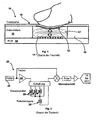
- Chandler, Ariz. Published an arrangement design 10 for inductive proximity switches (the "MICROCHIP design") which provides a magnetic coupling between a solid metal target 12 and an inductive measuring or sensing coil 14 separated by a spacer layer 16 are used.
- the spacer layer 16 defines a cavity or pocket into which the solid metal target 12 may flex when pressed, thereby printing and / or attaching its proximity to the sensor coil 14 attached to a PCB PCB 19 etched in such, and change the surrounding field.
- the front panel 18 also referred to as the top key switch layer or cover, may be the outermost skin of the product or home appliance, of which the keyboard is a part.
- the MICROCHIP design assumes that copper, aluminum, measurement, stainless steel, and mild steel are materials of choice for a cover layer / target combination, however, a target in accordance with the design could also be made of gold and / or silver as long as the material allows for physical deformation of the target over the sensor coil.
- Specific target embodiments disclosed in the MICROCHIP design include a copper cladding and one on the underside of the Cover set self adhesive or adhesive copper label.
- the MICROCHIP design states that, in general, the target 12 should have the size and shape of the sensor coil 14.
- a microcontroller is provided to periodically interrogate various sensors by measuring the impedance of a sensing coil. If the impedance of the sensing coil has changed, the microcontroller determines whether the change in impedance is sufficient to classify it as user pressure.
- the individual sensing coils ie, one for each switch
- the reference choke coil serving as the reference choke coil, allowing a ratio metric measurement that eliminates multiple drift sources.
- the inductive sensing circuit of the MICROCHIP design uses a single driver circuit to drive each of the sensing coils, each of which is connected by a common connection to the reference coil.
- the outer material of a key switch (the cover) is made of a relatively thick, for example, 0.032 to 0.036 inch thick piece of stainless steel.
- the cover is made of a relatively thick, for example, 0.032 to 0.036 inch thick piece of stainless steel.
- a 2.15 diameter measuring coil Customs require. Such a measuring coil diameter would be impractical for the landscape format of the device keyboard, ie would require a key spacing of more than 2 inches. It has also been found that with such materials, a drive current can be so high had to be that eddy currents are generated in the metal.
- the MICROCHIP design assumes that, as an alternative solution, the reference coil can be eliminated and provided to compensate for the drift software.
- the MICROCHIP design specifically discloses that such software can become bulky and the burden on the microcontroller may increase significantly, whereas the inclusion of the reference choke on the card is minimal, which is why the MICROCHIP design specifically states that omitting the reference coil is not recommended as soon as the increase in software size is considered.
- pressure-sensitive inductive switches are known from the US 2009/0160789 A1 and the DE 20 2008 001 970 U1 known.
- the present invention is therefore based on the problem, an arrangement and a system for a to provide inductive sensor switch that eliminates the disadvantages of the prior art.
- an arrangement for an inductive sensor switch comprising: a user interface front panel section; a sensor coil disposed on a circuit board; a conductive target disposed between the user interface panel section and the sensor coil; a frame disposed between the circuit board and the user interface front panel section, the frame including a bridging section having an uppermost surface adjacent the lower surface of the user interface front panel section and a lowermost surface facing the sensor coil , wherein the conductive target is located proximal to the lowermost surface of the bridging portion, whereby deflection of the faceplate portion above the frame results in deflection of the bridging portion and movement of at least a portion of the conductive target toward the sensor coil.
- a system for an inductive sensor key switch comprising: a plurality of inductive sensor key switch assemblies each of said inductive sensor key switch assemblies comprising a conductive target coupled to a sensor coil; a plurality of drive circuits that generate a drive current, each of the plurality of drive circuits comprising their own drive transistor, and wherein each of the plurality of drive circuits provides drive current to only one of the plurality of inductive sensor load switch arrangements.
- a system has several arrangements for an inductive sensor key switch, wherein each sensor coil is connected directly to ground via a common supply line connection.
- the assembly further comprises at least one light emitter disposed on the circuit board, and wherein at least a portion of the frame is made of a translucent material, wherein the translucent portion of the frame is in optical communication with an emitting portion of the at least one light emitter is arranged.
- the target is attached directly to the lowermost surface of a bridging section.
- the conductive target is fixed by hot stamping and / or printing to the lowermost surface of the bridging section.
- the frame further comprises a bead portion projecting from the bridging portion, the conductive target being disposed away from the bridging portion in communication with the bead portion.
- the conductive target is attached to the distal bead portion and floats over the sensor coil.
- the conductive target is a metal disc.
- the conductive target is a sheet of a multi-leaf target.
- the conductive target is a conductive cap which is mounted between the circuit board and the bead portion and above the sensor coil on the circuit board.
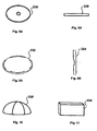
- the conductive cap is either a dome-shaped or a box-shaped or a footed disc.
- the sensor coil comprises a first set of windings which rotate in a first direction and a second set of windings which rotate in a second direction, the second direction being opposite to the first direction, the second set of windings surrounds the first set of turns.
- the sensor coil comprises a first set of turns, the arrangement further comprising at least one additional turn disposed outside the first set of turns, the at least one additional turn being shorted to a reference potential.
- At least one sensor coil is a multi-level sensor coil.
- the inductive sensor load switch arrangement comprises: a user interface front panel section; a sensor coil disposed on a first circuit board; a conductive target disposed between the user interface front panel section and the sensor coil; a second circuit board disposed between the first circuit board having the sensor coil and the user interface front panel section; a frame disposed between the second circuit board and the user interface front panel section, the frame including a bridging section having an uppermost surface adjacent to a lower surface of the user interface front panel section and a lowermost surface facing the uppermost surface of the user interface PCB, wherein the frame further comprises a bead portion which is from the bottom surface of the bridging portion, wherein the distal portion of the bead portion to a portion of the uppermost surface of the second printed circuit board adjacent to or is arranged in connection therewith the conductive target is disposed on a portion of a lower surface of the second circuit board below the bead portion such that flexing of the user interface front panel portion above the frame results in deflection of the a
- each of the plurality of drive circuits is disposed on the circuit board local to that arrangement for the inductive sensor key switch to which it provides a drive current.
- At least one of the plurality of sensor inductive sensing switch assemblies includes a faceplate portion, the conductive target being adjacent but spaced apart from the sensor coil of the at least one inductive proximity sensing switch assembly, the sensor coil being disposed on a printed circuit board.
- a second printed circuit board is arranged between the printed circuit board with the sensor coil and the front panel section and a frame between the second printed circuit board and the front panel section.
- the frame comprises a bridging portion having an uppermost surface adjacent to a lower surface of the faceplate portion and a lowermost surface facing the second printed circuit board.
- the frame comprises a bead portion that projects from the bottom surface of the bridging portion, wherein the distal portion of the bead portion is adjacent to or communicating with a portion of a front surface of the second printed circuit board.
- the conductive target is disposed at a portion of a back surface of the second circuit board below the bead portion so that deflection of the panel portion above the frame results in deflection of the panel Bridging portion results whose force is transferable through the bead portion on the second circuit board, whereby the second circuit board is bendable and the coupling of the conductive target is changeable with the sensor coil.
- each inductive sensor key assembly includes a translucent key element supported by a frame, the target being disposed on a rearward outer surface of the translucent key element.
- an improved inductive sensor switch is provided.
- a circuit for inductive sensing switches that eliminates the reference inductor without requiring the addition of extensive software.
- the present invention relates to an inductive sensor key switch and its associated control circuit, the inductive sensor key user interface being suitable for use with a control circuit having driver elements spatially associated with the respective key switch.
- an arrangement and circuit for inductive sensor switches are provided which, under certain circumstances, can be used to control both signal strength and signal strength Noise immunity of the present invention over those of the MICROCHIP design.
- Fig. 2 a block diagram of a system 20 for inductive sensor key switch of the prior art in accordance with the teachings of the MICROCHIP design shown.
- the system 20 To measure the impedance of a respective sensor or measuring coil 26, the system 20 generates a pulse at the pulse width modulator (PWM) 22 which is converted by the driver 24 into a drive pulse which is used to energize a respective sensor coil 26 again.
- PWM pulse width modulator
- the pulse voltage from the sensor coil 26 is further processed and analyzed to determine if there has been a change in impedance indicating contact by the user.
- PWM pulse width modulator
- the sensor coils 26 are each connected at one end to a reference coil 28 via a single common connection.
- the connection with such a reference coil forces the creation of long PCB design paths which, especially with long keyboards, pick up the noise and reduce the signal strength.
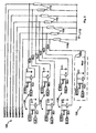
- a particular embodiment of a circuit 100 for inductive sensor keyswitches of the present invention is shown which provides for improved noise immunity and enhanced signal strength transmission.
- the number of long, noisy paths inherent in the prior art system is greatly reduced.
- each of the sensor coils 110 of the system 100 is connected to the common connection directly (ie not via any other series connected circuit element) to ground 112 and not to a reference coil, eliminating the need to route each sensor coil one path to a common one Pull reference coil.
- no energy goes to the reference coil, causing the ratio change when a key press is detected is reduced.
- software filtering to compensate for the drift is added instead of the omitted reference coil.
- the circuit 100 also eliminates long paths from a common driver circuit to each sensor coil 110 by providing individual drive or driver circuits 120 for energizing the respective coils 110.
- each of the driver circuits 120 is provided locally (ie, in close proximity) to the sensor coil 110 that drives it.
- the driver circuit 120a is disposed near the sensor coil 110a on the PCB.
- the remainder of the individual driver circuits 120 are located on the printed circuit board (PCB) near its associated sensor coil 110, which is driven by the single driver circuit 120.
- PCB printed circuit board
- the metal forming the sensor coil 162 is placed next to the metal traces 166 and contacts or pads 164 for the driver circuit elements (ie, a driver transistor, one or more input resistors, one or more output resistors, etc.) on the PCB.
- the driver circuit elements ie, a driver transistor, one or more input resistors, one or more output resistors, etc.
- the metallization for the contacts for the driver coil associated with that sensor coil 162 is located at most a few millimeters from the outermost turn of the sensor coil 162, thus shortening the lead lengths between a drive circuit and the sensor coil 162 driving it can.
- each of the plurality of drive circuits 120 includes its own driver transistor T1 and resistor and capacitor elements used to define the drive current.
- each of the driver circuits 120 comprises at least one driver transistor T1, a first input resistor connected between the base of the transistor T1 and a clock input for the respective driver circuit 120 Rin1, a second input resistor Rin2 connected between the base of T1 and a DC power supply, an output resistance Rout, and a capacitor C1.
- Rin1 is 470 ohms
- Rin2 is 100 ohms
- Rout is 270 ohms
- C1 is 1 ⁇ F
- the power supply is 5 volts DC.
- inductors 110 is selected based on a number of factors including the outside radius of the coil, the number of turns in the coil, and the depth of the coil. Each sensor coil 110 is connected via an in Figure 3 Scanned output shown periodically scanned by a microcontroller or microprocessor (not shown). It should be noted that although the transistor T1 is shown as a pnp transistor, this is not to be construed restrictively, since the circuit can be adapted to the use of an npn transistor.
- each sensor coil 110 of this embodiment is driven by only one driver circuit 120, and conversely, each driver circuit 120 drives only one associated sensor coil 110.
- Locally locating each of a plurality of drive circuits to their associated one of the sensor coils results in a small circuit through the sensor coil of each key array without greatly radiating current / noise from the coil to the outside. The less current / noise emitted by the coil to the outside, the less it can be absorbed by other sensor coils.
- the noise pickup by the coil can be further reduced by taking a short turn outside of the PCB film Coil is added. This may slightly reduce the signal strength; however, since it is outside the coil surface and the coil-induced field is concentrated near the coil pattern, it does not cause much signal strength reduction. However, the shortened turn reduces uniform external fields as they come from outside the coil pattern.
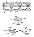
- the noise pick-up by the sensor coil can be further reduced by adding turns outside the sensor coil as an extension of the sensor coil, but in the opposite direction. See for example Figure 17 where the turns 510 of the sensor coil 500 rotate in a first direction, but the other way around the turn section 515 to have multiple turns 520 in the opposite direction.
- the use of such additional turns 520 reduces the field strength such that, relative to external fields, the loop surface of the sensor coil minus the loop surface of the turns leads in the opposite direction to a take-up by (N coil-x reverse turns) 2 . It should be noted that only a few large opposing turns equal the loop area of many small turns in the coil.
- Fig. 18 is now another embodiment of a multi-level or multi-layer sensor coil 530 used as a sensor coil in a system in FIG Agreement can be used with the present invention shown.
- the multilayer sensor coil 530 includes two individual sensor coils 540, 550 overlapping each other on the surface of the PCB (not shown) and sharing the commonly connected input and output contacts 542, 552 and 544, 554.
- the coil 550 is wound in a direction opposite to that of the coil 540 and covers the coil 540 on the PCB.
- Both input contacts 542 are connected to a measuring input (for example in FIG Fig. 3 shown) of a microcontroller or microprocessor (not shown) programmed to evaluate the measurements made on the sensor coil 530.
- the output contacts 544 and 554 are connected to a common reference potential, such as ground.
- the multilayer coil provides greater field strength and better eddy currents that result in better signal return when target movement occurs.
- the PCB may further include staggered vias to avoid blind vias and help keep costs low. It should be noted that although in the explanatory illustration of FIG Fig. 18 two coils are shown, this is not to be construed restrictive, since more coil layers can be provided as needed. Note, however, increasing the number of coil layers in the sensor coil 530 decreases the distance between the uppermost surface of the sensor coil 530 and the target portion of the key switch, due to the increased thickness of the layers on the PCB. In order to accommodate the increased layer height at the PCB, an appropriate adjustment to the distance between the uppermost coil layer and the target can be made as needed.
- the driver circuits 120 can be configured as needed to allow for driver-to-key variations in driver strength. For example, differently sized keys (and their associated coils) may have different signal strength levels need.
- the drive voltage can be changed from one sensor coil / sensor key coordination to the other by a fixed value. Alternatively, as needed, the drive voltage may be changed from one sensor to another as a software variable using an adaptive algorithm.
- Another advantage of associating the driver 120 with the location of the associated sensor coil 110 is that the delay of the drive pulse can be optimized to bring all useful signals into the detector as compared to a synchronous detector system.
- the delay can be greatly improved by offsetting the driver transistor and the sense resistor to the coil location since previous drive pulse delay times were affected by temperature variation and part deviation.
- coils may be stacked in double-sided PCBs.
- four coil layers were stacked by offsetting the via to avoid hidden vias.
- a sensor inductive load switch assembly 200 that provides improved signal strength and mechanical stability in a sensor inductive load switch system in accordance with a particular embodiment of the present invention.
- the key switch assembly 200 of this embodiment is located under a portion of the front panel or cover 218 (ie, the keyboard, product, and / or home appliance front panel) that defines a user interface push-button.
- the front panel 218 and thus the user interface is one thin stainless steel plate.
- the prior art push-button assembly illustrated in FIG. 2 does not staple the target 212 of the key switch assembly 200 to the underside of the cover 218, but instead supports it with a frame 216 disposed between the cover 218 and the PCB 219.
- the frame 216 is formed as a bracket or pocket defining a space or cavity 217 about the sensor coil 214.
- the frame 216 is a separate, separate piece made of plastic and includes a support bracket 216 surrounding the sensor coil 214, at the top of which is a bridging portion 216a located at a location defining a push-button on the user interface of the front panel 218.
- a support bracket 216 surrounding the sensor coil 214, at the top of which is a bridging portion 216a located at a location defining a push-button on the user interface of the front panel 218.
- a bridging portion 216a located at a location defining a push-button on the user interface of the front panel 218.
- the support bracket 216 may be made as a frame (i.e., four feet or four walls, etc.) or in the form of a ring covered by the bridging portion 216a. This frame may be connected to the PCB 216 by screws, hot-inserted connectors, or other conventional connection methods.
- the bridging portion 216a is designed of very thin plastic so that the deflection of the cover 218 results in a deflection of the bridging portion 216a.
- the thickness "A" of the bridging portion 216a is 0.8 mm.
- the metal target 212 on the underside of the bridging portion is also deflected, thereby changing between the target 212 and the sensor coil 214, indicating depression of the key switch.
- the target 212 is supported by a structure that exists between the Front panel cover 218 and the PCB 219 is arranged, and not directly attached to the underside of the front panel cover 218.
- the target 212 of the key switch assembly 200 is instead attached to the underside of the bridging portion 216a to bring the target 212 into the desired relationship with the sensor coil 214.
- the target 212 is attached to the underside of the bridging section as part of a hot stamping process.
- the target 212 may be attached to the underside of the bridging portion 216a by printing the target directly on the back of the cover to provide a metal surface over the sensor coil.
- a hot stamped film or conductive print material may be applied to the frame 216 by any suitable process (i.e., hot stamping, printing, etc.). Hot stamping or printing of the target 212 onto a surface of the frame 216 rather than the cover 218 may be particularly useful in applications where adjacent lighting is needed and / or curved surfaces are used.
- a portion of the front panel 218 defines a user interface or keyboard for a product or home appliance.
- a metal foil is embossed on the inner surface of the plastic bracket or bag.
- the film desirably has a thickness between 0.05 mm and 0.1 mm.
- the conventional PCB-based keypads are replaced by a hot-stamped foil or printed conductive layer supported by a separate yoke.
- a printing process may be used to apply a conductive material to the underside of the substrate Bridging section 216a to print.
- the thickness of the printed material would be similar to that for the hot embossed film, ie most preferably between 0.05 mm and 0.1 mm.
- a key switch assembly 220 in accordance with the present invention is shown.
- the key switch assembly 220 is similar to the key switch assembly 200 of FIG Figure 4 however, it is directed to a user interface having push buttons with any type of illuminated sign such as words, light rings, and / or other light indicators, but having an opaque plate.
- the key switch assembly 220 includes a target 212 attached to the bridging portion 226a of a frame 226 in a particular plane with respect to a sensor coil 214.
- the deflection of the key switch cover 228 results in the deflection of the bridge portion 226a which alters the coupling between the target 212 and the sensor coil 214, thus indicating a key depression of the key switch cover 228.
- the frame 226 of this embodiment is made of clear or other translucent plastic so that light emitted by a light source can be transmitted to the ring, words, or characters on the user interface.
- a light source ie, incandescent lamp, electroluminescent source, etc.
- the light source includes light emitting diodes (LEDs) 230 mounted on the underside of the PCB 229.
- the plastic frame comprises a translucent ring portion 226b surrounding an opaque key switch cover 228.
- the key switch cover 228 may itself have stamped portions such as words or other indicia intended to be illuminated.
- Light emitted by the LEDs 230 is used to label the ring and / or the characters follows to illuminate.
- the light from the LEDs 230 passes through the PCB 229 through holes 222 in the PCB 229 that are adjacent to the light emitting side of the LEDs.
- the holes 222 open into the cavity 227 formed in the frame between the target 212 and the sensor coil 214.
- the frame 226 may optionally include facets 226c, particularly arranged to direct and concentrate light emitted by the LEDs 230 into the cavity 227 on the light ring portions 226b.
- the frame 226 may include opaque or opaque portions 224 as needed to prevent the light emitted in conjunction with a key switch assembly from being transferred to another key switch assembly.
- a white coating is applied to the PCB 226 disposed in the cavity 227 to further reflect light from the cavity 227 into the translucent frame 226.
- the target 212 of the key switch assembly 220 may be variously including, but not limited to, hot stamping the target 212 onto the frame 226 and / or printing the target 212 onto the frame 226 using a conductive ink at Frame 226 may be attached. It should be noted that, if desired, the target 212 may also be formed as a metal disc or foil adhered to the underside of the bridging portion 226a without departing from the spirit of the present invention.
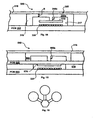
- the key switch assembly 300 includes a frame 310 disposed between the PCB 302 and the front panel 318 of the user interface of a device, which is in communication with Fig. 4 frame 216 is similar.
- the frame 310 of the assembly 300 includes a bridging portion 310a that is adjacent to and in contact with the underside of the front panel 318 at a location defining a key switch on the front panel 318.
- the bridging portion is preferably made of a thin plastic material having a thickness "B" that allows it to deflect in response to the deflection of the face plate 318. In a particular embodiment, the dimension "B" is 0.8 mm.
- the frame 310 also includes a push pin or bead 310b that extends from the center of the bridging portion 310a toward the sensor coil 320.
- the target 330 communicates with the distal end of the bead 310b and has a circumference larger than the circumference of the sensor coil 320 so as to circumscribe the sensor coil 320.
- deflection of the front panel 318 over the bridging portion 310a causes the pusher pin 310b to push a portion of the target 330, thus deflecting the target 330 and altering the coupling between the target 330 and the sensor coil 320, indicating depression of the key switch .
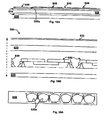
- the target 330 as a hood-shaped cap, which in Fig. 10 is shown more clearly formed.
- a footed "disk" 332 which instead of the target 330 of Fig. 6 on the PCB 302 may be surface mounted (via the extending foot portions), wherein the deflection of the face plate 318 above the frame 310 causes the bead 310b to deflect the feet washer 332 and thus the coupling between the target 332 and the sensor coil 320 changed, indicating that one Push-button is pressed.
- the footed disc 332 from the Figs. 9A and 9B may be formed by chemical etching and / or embossing of the metal to be used as a target.
- a target 334 having the shape of a square or rectangle may be placed over the sensor coil 320 and deflected by the front panel 318 above the frame 310 Bead 310b are activated.
- a sensor load switch assembly 340 which uses a frame 350 having a bead 350a to transmit the deflection of the key switch cover 228 to the target 330 mounted on the PCB, using light from a light source, the LEDs 230 in this embodiment, passes through holes 222 in the PCB 355.
- the frame 350 is made of a translucent material such as a clear plastic. The frame 350 is therefore aligned with the holes 222 to cause light to project from the ring portions 350b as well as any words or characters punched into the key switch cover 228.
- LEDs 230 and the holes 222 may be arranged such that in the same manner as in connection with the frame 226 of FIG Fig. 5 has been described, the central cavity 317 of the frame 350 and thereby the frame 350 and the ring portions 350b are illuminated.
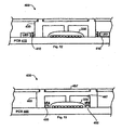
- FIGS. 12 and 13 There are now two further illuminated key switch assemblies 400 and 430, respectively, in accordance with further embodiments of the present invention Invention shown. Exactly shows Fig. 12 a key switch assembly 400 in which LEDs 410 are mounted on the front of the PCB 415, with their light-emitting outer surfaces facing the sidewalls of the frame 420. In Fig. 13 For example, the LEDs 450 on the PCB 445 are surface mounted in the cavity 447 of the frame 440 with their light emitting outer surfaces facing the front panel 457. From the foregoing, it will be understood that other configurations of a lighting key switch assembly may be implemented by means of a translucent frame in conjunction with a target in accordance with the present invention.
- FIG. 14 Now another embodiment of a key switch assembly 500 in accordance with the present invention is shown.
- the key switch assembly 500 is similar in many ways to the key switch assembly 300 of FIG Fig. 6 , However, instead of using a surface mounted target sandwiched between the bead and the PCB, as in the key switch assembly 200, this embodiment uses a floating target 510 attached to the bead 310b. Thus, deflection of the bridging portion 310a, rather than causing the target 510 to deflect, causes the target closer to the sensor coil 214, whereby its field is changed and a key press is displayed.
- the target 510 is a cut-out or punched-out disk, such as those shown in FIGS Figs. 8A and 8B
- the diameter of the disc 338, 510 may be selected as needed, but is preferably equal to or greater than the diameter of the sensor coil 320.
- the floating target 510 of FIG Fig. 14 can be used in a light key arrangement.
- the floating target 510 may include the surface mounted target 330 in the key switch assembly 340 of FIG Fig. 7 or in any other embodiment described herein.
- FIG. 15 Now, another embodiment of a sensor inductive switch 550 arrangement in accordance with the present invention is shown.
- the frame 560 instead of being disposed between and in communication with the PCB 555 and the front panel 318, the frame 560 is sandwiched between a ground plane PCB 565 and the front panel 318 that overlies the PCB 555 that supports the sensor coil 320 arranged.
- the ground plane PCB 565 is separated from the PCB 555 by a spacer 570 having a circular cut-out over the sensor coil 320, creating a cavity or chamber over the sensor coil 320.
- the frame 560 is supported by its outer wall portions over solid portions of the spacer layer on the ground plane PCB 565, whereby the frame 560 is supported when a push button switch indicated on the face plate 318 above the assembly 550 is pressed.
- the frame also has a bead 560a extending from its central portion, which is in contact with a portion of the ground plane PCB 565. Deflection of the front panel 318 above the bead 560a causes the bead 560a to deflect the PCB 565.
- the portion of the PCB 565 disposed below the bead 560a includes a metal target 570 located at the bottom thereof adjacent the sensor coil 320.
- the deflection of the front panel 318 is transmitted through the frame 560 to the target 570, which facilitates coupling between the target 570 and the sensor coil 320 changes, indicating that a pushbutton located above the user interface assembly has been pressed.
- the target 570 is either printed on or hot stamped onto the lower surface of the PCB 565. It should be noted that other methods of applying the target 570 to the PCB 565 including all methods of creating a metallization of a PCB.
- the keyboard 600 includes a plurality of illuminated key switches 640, where the key switch elements 640 serve as both optical fibers for transmitting the light through the cover or faceplate 610 and as a force translator for moving the target with respect to the sensor coil.
- a backlit pushbutton 640 is provided having light bulges 640a forming a light ring and passing through apertures 610a in the opaque faceplate 610.
- the key switch elements 640 are held in place in a frame 620 disposed between the front panel 610 and a PCB 630.
- the frame 620 may be secured by the adhesive layers 615 disposed between the frame 620 and the PCB 630 and the frame 620 and the face plate 610. As in the previous embodiments, each key switch is disposed over a corresponding sensor coil disposed on the PCB 630 in the frame. The frame 620 may be aligned as needed by the alignment pins 622 with respect to the front panel 610.
- Each key switch element 640 is designed to mate with an opening 620a of the frame 620 with the light transmitting protrusions 640 passing through the front panel 610 of the assembly 600.
- a flat outer surface 640c of the key switch element 640 is provided to support an adhesive layer and / or the front panel 610.
- the key switch member 640 is held in the frame by the tabs 640b and the groove 640e, which engage the rear of the frame 620, that is, the side remote from the front outer surface 610 (as in FIG Fig. 20B is shown).
- a target in the Fig. 19 - 21 not shown
- the target is a piece of metal foil bonded to the rear outer surface 640d.
- each key switch element 640 is supported over a sensor coil by the frame 620 and / or an adhesive layer 612 (which does not pass under the portion of the key switch element 640 that includes the target).
- the target on the rearward outer surface 640d of each key switch element 640 is disposed in the desired relationship with a sensor coil, as has been described elsewhere herein.
- the inductive keying circuit of the present invention may be modified to include a reference coil implemented at a key position of the keyboard.
- the reference coil is used to provide drift compensation as a standard reference, with no key movement is allowed to assist.
Landscapes
- Push-Button Switches (AREA)
- Switches That Are Operated By Magnetic Or Electric Fields (AREA)
- Electronic Switches (AREA)
Claims (19)
- Agencement pour un bouton-poussoir de détection inductif qui comprend :une section de platine avant d'interface d'utilisateur (18, 218, 218', 318, 457, 610) ;une bobine de détection (14, 26, 110, 110a, 162, 214, 320, 510, 515, 520, 530, 540, 550) qui est disposée sur une carte de circuit imprimé (19, 219, 229, 302, 355, 415, 445, 555, 630) ;une cible conductrice (12, 212, 330, 332, 334, 338, 510, 570) qui est disposée entre la section de platine avant d'interface d'utilisateur (18, 218, 218', 318, 457, 610) et la bobine de détection (14, 26, 110, 110a, 162, 214, 320, 510, 515, 520, 530, 540, 550) ;un cadre (216, 226, 310, 350, 420, 440, 560, 620) qui est disposé entre la carte de circuit imprimé (19, 219, 229, 302, 355, 415, 445, 555, 630) et la section de platine avant d'interface d'utilisateur (18, 218, 218', 318, 457, 610)caractérisé en ce que le cadre (216, 226, 310, 350, 420, 440, 560, 620) comprend une section de pontage (216a, 226a, 310a) qui possède une surface la plus haute qui est adjacente à la surface inférieure de la section de platine avant d'interface d'utilisateur (18, 218, 218', 318, 457, 610) et une surface la plus basse qui est tournée vers la bobine de détection (14, 26, 110, 110a, 162, 214, 320, 510, 515, 520, 530, 540, 550), etpour lequel la cible conductrice (12, 212, 330, 332, 334, 338, 510, 570) est disposée le plus proche de la surface la plus basse de la section de pontage (216a, 226a, 310a) par laquelle une flexion de la section de platine avant (18, 218, 218', 318, 457, 610) conduit par le cadre (216, 226, 310, 350, 420, 440, 560, 620) à une flexion de la section de pontage (216a, 226a, 310a) et à un mouvement d'au moins une section de la cible conductrice (12, 212, 330, 332, 334, 338, 510, 570) à la bobine de détection (14, 26, 110, 110a, 162, 214, 320, 510, 515, 520, 530, 540, 550).
- Agencement selon la revendication 1 caractérisé en ce qu'un système (100) présente plusieurs agencements pour un bouton-poussoir de détection inductif (200, 220, 300, 340, 400, 430, 500, 550, 600) pour lequel chaque bobine de détection (14, 26, 110, 110a, 162, 214, 320, 510, 515, 520, 530, 540, 550) est reliée directement à la terre (112) par une liaison d'alimentation commune.
- Agencement selon la revendication 1 ou 2 caractérisé en ce que l'agencement (200, 220, 300, 340, 400, 430, 500, 550, 600) comprend en plus au moins un émetteur de lumière (230, 330, 410, 450) qui est disposé sur la carte de circuit imprimé (19, 219, 229, 302, 355, 415, 445, 555, 630) et pour lequel au moins une section du cadre (216, 226, 310, 350, 420, 440, 560, 620) est fabriquée en matériau transparent, pour lequel la section transparente du cadre (216, 226, 310, 350, 420, 440, 560, 620) est disposée en liaison optique avec une section émettrice de l'au moins un émetteur de lumière (230, 330, 410, 450).
- Agencement selon une quelconque des revendications précédentes caractérisé en ce que la cible (12, 212, 330, 332, 334, 338, 510, 570) est fixée directement à la surface la plus basse de la section de pontage (216a, 226a, 310a).
- Agencement selon la revendication 4 caractérisé en ce que la cible conductrice (12, 212, 330, 332, 334, 338, 510, 570) est fixée par estampage à chaud et/ou impression à la surface la plus basse de la section de pontage (216a, 226a, 310a).
- Agencement selon la revendication 4 caractérisé en ce que le cadre (216, 226, 310, 350, 420, 440, 560, 620) comprend en plus une section à bourrelet (310b, 350a, 560a) qui descend de la section de pontage (216a, 226a, 310a), pour lequel la cible conductrice (12, 212, 330, 332, 334, 338, 510, 570) est disposée loin de la section de pontage (216a, 226a, 310a) en liaison avec la section à bourrelet (310b, 350a, 560a).
- Agencement selon la revendication 6 caractérisé en ce que la cible conductrice (12, 212, 330, 332, 334, 338, 510, 570) est fixée sur la section à bourrelet (310b, 350a, 560a) éloignée et est en suspension au-dessus de la bobine de détection (14, 26, 110, 110a, 162, 214, 320, 510, 515, 520, 530, 540, 550).
- Agencement selon la revendication 6 caractérisé en ce que la cible conductrice (12, 212, 330, 332, 334, 338, 510, 570) est un capuchon conducteur (330, 334) qui est monté entre la carte de circuit imprimé (19, 219, 229, 302, 355, 415, 445, 555, 630) et la section à bourrelet (310b, 350a, 560a) et au-dessus de la bobine de détection (14, 26, 110, 110a, 162, 214, 320, 510, 515, 520, 530, 540, 550) au niveau de la carte de circuit imprimé (19, 219, 229, 302, 355, 415, 445, 555, 630).
- Agencement selon la revendication 1 caractérisé en ce que la bobine de détection (14, 26, 110, 110a, 162, 214, 320, 510, 515, 520, 530, 540, 550) comprend un premier jeu de spires (510, 540) qui tournent dans une première direction et un deuxième jeu de spires (520, 550) qui tournent dans une deuxième direction, la deuxième direction étant opposée à la première direction, le deuxième jeu de spires (520, 550) entourant le premier jeu de spires (510, 540).
- Agencement selon la revendication 1 caractérisé en ce que la bobine de détection (14, 26, 110, 110a, 162, 214, 320, 510, 515, 520, 530, 540, 550) comprend un premier jeu de spires (510), l'agencement (200, 220, 300, 340, 400, 430, 500, 550, 600) comprenant en plus au moins une spire supplémentaire (520) qui est disposée en dehors du premier jeu de spires (510), l'au moins une spire supplémentaire (520) étant court-circuitée à un potentiel de référence.
- Agencement selon une quelconque des revendications précédentes caractérisé en ce qu'au moins une bobine de détection (14, 26, 110, 110a, 162, 214, 320, 510, 515, 520, 530, 540, 550) est une bobine de détection multiniveau (530).
- Système pour un bouton-poussoir de détection inductif qui comprend :plusieurs agencements pour un bouton-poussoir de détection inductif (200, 220, 300, 340, 400, 430, 500, 550, 600) selon une quelconque des revendications 1 à 11,pour lequel chacun des agencements pour le bouton-poussoir de détection inductif (200, 220, 300, 340, 400, 430, 500, 550, 600) comprend une cible conductrice (12, 212, 330, 332, 334, 338, 510, 570) qui est couplée avec une bobine de détection (14, 26, 110, 110a, 162, 214, 320, 510, 515, 520, 530, 540, 550),plusieurs circuits pilotes (120) qui produisent un courant d'attaque, chacun des plusieurs circuits pilotes (120) comprenant son propre transistor pilote (T1) etchacun des plusieurs circuits pilotes (120) ne fournissant un courant d'attaque qu'à un des plusieurs agencements pour le bouton-poussoir de détection inductif (200, 220, 300, 340, 400, 430, 500, 550, 600).
- Système selon la revendication 12 caractérisé en ce que chacun des plusieurs circuits pilotes (120) est localement disposé sur la carte de circuit imprimé (19, 219, 229, 302, 355, 415, 445, 555, 630) à chaque agencement pour le bouton-poussoir de détection inductif (200, 220, 300, 340, 400, 430, 500, 550, 600) auquel il fournit un courant d'attaque.
- Système selon la revendication 12 ou 13 caractérisé en ce qu'au moins un des plusieurs agencements pour un bouton-poussoir de détection inductif (200, 220, 300, 340, 400, 430, 500, 550, 600) comprend une section de platine avant (18, 218, 218', 318, 457, 610) pour lequel la cible conductrice (12, 212, 330, 332, 334, 338, 510, 570) est adjacente à la bobine de détection (14, 26, 110, 110a, 162, 214, 320, 510, 515, 520, 530, 540, 550) de l'au moins un agencement pour un bouton-poussoir de détection inductif (200, 220, 300, 340, 400, 430, 500, 550, 600), mais est toutefois disposée à distance de celle-ci, la bobine de détection (14, 26, 110, 110a, 162, 214, 320, 510, 515, 520, 530, 540, 550) étant disposée sur une carte de circuit imprimé (19, 219, 229, 302, 355, 415, 445, 555, 630).
- Système selon la revendication 14 caractérisé en ce qu'une deuxième carte de circuit imprimé (565) est disposée entre la carte de circuit imprimé (19, 219, 229, 302, 355, 415, 445, 555, 630) avec la bobine de détection (14, 26, 110, 110a, 162, 214, 320, 510, 515, 520, 530, 540, 550) et la section de platine avant (18, 218, 218', 318, 457, 610) et un cadre (216, 226, 310, 350, 420, 440, 560, 620) est disposé entre la deuxième carte de circuit imprimé (565) et la section de platine avant (18, 218, 218', 318, 457, 610).
- Système selon la revendication 15 caractérisé en ce que le cadre (216, 226, 310, 350, 420, 440, 560, 620) comprend la section de pontage (216a, 226a, 310a) qui présente une surface la plus haute qui est adjacente à une surface inférieure de la section de platine avant (18, 218, 218', 318, 457, 610) et une surface la plus basse qui est tournée vers la deuxième carte de circuit imprimé (565).
- Système selon la revendication 15 ou 16 caractérisé en ce que le cadre (216, 226, 310, 350, 420, 440, 560, 620) comprend une section à bourrelet (310b, 350a, 560a) qui descend de la surface la plus basse de la section de pontage (216a, 226a, 310a), la section éloignée de la section à bourrelet (310b, 350a, 560a) étant adjacente à une section d'une surface avant de la deuxième carte de circuit imprimé (565) ou étant disposée en liaison avec celle-ci.
- Système selon la revendication 17 caractérisé en ce que la cible conductrice (12, 212, 330, 332, 334, 338, 510, 570) est disposée sur une section d'une surface arrière de la deuxième carte de circuit imprimé (565) sous la section à bourrelet (310b, 350a, 560a) de sorte qu'une flexion de la section de platine avant (18, 218, 218', 318, 457, 610) conduit au-dessus du cadre (216, 226, 310, 350, 420, 440, 560, 620) à une flexion de la section de pontage (216a, 226a, 310a) dont la force est transmissible par la section à bourrelet (310b, 350a, 560a) à la deuxième carte de circuit imprimé (565), la deuxième carte de circuit imprimé (565) étant de ce fait fléchissable et le couplage de la cible conductrice (12, 212, 330, 332, 334, 338, 510, 570) à la bobine de détection (14, 26, 110, 110a, 162, 214, 320, 510, 515, 520, 530, 540, 550) étant modifiable.
- Système selon une quelconque des revendications précédentes caractérisé en ce que chaque agencement pour le bouton-poussoir de détection inductif (200, 220, 300, 340, 400, 430, 500, 550, 600) comprend un élément poussoir transparent qui est supporté par un cadre (216, 226, 310, 350, 420, 440, 560, 620), la cible (12, 212, 330, 332, 334, 338, 510, 570) étant disposée sur une surface extérieure arrière de l'élément poussoir transparent.
Priority Applications (2)
| Application Number | Priority Date | Filing Date | Title |
|---|---|---|---|
| PL11703823T PL2529484T3 (pl) | 2010-01-29 | 2011-01-31 | Układ i system indukcyjnego wyłącznika czujnikowego |
| EP20130003703 EP2660980A2 (fr) | 2010-01-29 | 2011-01-31 | Agencement et système pour un bouton-poussoir de détection inductif |
Applications Claiming Priority (2)
| Application Number | Priority Date | Filing Date | Title |
|---|---|---|---|
| US12/696,458 US20110187204A1 (en) | 2010-01-29 | 2010-01-29 | Inductive touch key switch system, assembly and circuit |
| PCT/EP2011/000426 WO2011092033A2 (fr) | 2010-01-29 | 2011-01-31 | Agencement et système pour bouton-poussoir de détection inductif |
Related Child Applications (1)
| Application Number | Title | Priority Date | Filing Date |
|---|---|---|---|
| EP13003703.9 Division-Into | 2013-07-24 |
Publications (2)
| Publication Number | Publication Date |
|---|---|
| EP2529484A2 EP2529484A2 (fr) | 2012-12-05 |
| EP2529484B1 true EP2529484B1 (fr) | 2013-12-25 |
Family
ID=44319893
Family Applications (2)
| Application Number | Title | Priority Date | Filing Date |
|---|---|---|---|
| EP20110703823 Not-in-force EP2529484B1 (fr) | 2010-01-29 | 2011-01-31 | Agencement et système pour bouton-poussoir de détection inductif |
| EP20130003703 Withdrawn EP2660980A2 (fr) | 2010-01-29 | 2011-01-31 | Agencement et système pour un bouton-poussoir de détection inductif |
Family Applications After (1)
| Application Number | Title | Priority Date | Filing Date |
|---|---|---|---|
| EP20130003703 Withdrawn EP2660980A2 (fr) | 2010-01-29 | 2011-01-31 | Agencement et système pour un bouton-poussoir de détection inductif |
Country Status (4)
| Country | Link |
|---|---|
| US (1) | US20110187204A1 (fr) |
| EP (2) | EP2529484B1 (fr) |
| PL (1) | PL2529484T3 (fr) |
| WO (1) | WO2011092033A2 (fr) |
Cited By (6)
| Publication number | Priority date | Publication date | Assignee | Title |
|---|---|---|---|---|
| WO2015172863A1 (fr) | 2014-05-13 | 2015-11-19 | Diehl Ako Stiftung & Co. Kg | Dispositif de commande, notamment pour un appareil électroménager |
| DE102014015003A1 (de) | 2014-10-09 | 2016-04-14 | Diehl Ako Stiftung & Co. Kg | Bedienvorrichtung, insbesondere für ein elektronisches Haushaltsgerät |
| DE102015009781A1 (de) | 2015-07-24 | 2017-01-26 | Diehl Ako Stiftung & Co. Kg | Bedienvorrichtung, insbesondere für ein elektronisches Haushaltsgerät |
| DE102015014245A1 (de) | 2015-11-04 | 2017-05-18 | Diehl Ako Stiftung & Co. Kg | Bedienvorrichtung, insbesondere für elektronische Haushaltsgeräte |
| DE102016004220A1 (de) | 2016-04-07 | 2017-10-12 | Diehl Ako Stiftung & Co. Kg | Bedienvorrichtung, insbesondere für ein elektronisches Haushaltsgerät |
| WO2017174097A1 (fr) | 2016-04-07 | 2017-10-12 | Diehl Ako Stiftung & Co. Kg | Dispositif de commande, en particulier pour appareil domestique |
Families Citing this family (21)
| Publication number | Priority date | Publication date | Assignee | Title |
|---|---|---|---|---|
| US20120242515A1 (en) * | 2011-03-24 | 2012-09-27 | Diehl Ako Stiftung & Co. Kg | Inductive touch sensing circuit providing sensitivity compensation |
| DE102011075942A1 (de) * | 2011-05-16 | 2013-05-16 | E.G.O. Elektro-Gerätebau GmbH | Bedieneinrichtung für ein Elektrogerät und Elektrogerät |
| EP2721627A4 (fr) * | 2011-05-27 | 2015-04-15 | Diehl Ako Stiftung Gmbh & Co | Système de commutateur à touches tactiles par induction comprenant un mécanisme de déplacement en translation de déflexion |
| US9214936B2 (en) * | 2013-06-18 | 2015-12-15 | Hyundai Motor Company | Non-contact sensing module and method of manufacturing the same |
| WO2016138546A2 (fr) | 2015-02-27 | 2016-09-01 | Azoteq (Pty) Ltd | Détection d'inductance |
| US9746168B1 (en) * | 2015-10-30 | 2017-08-29 | American Opto Plus Led Corporation | Light-emitting touch buttons |
| CN107204763A (zh) * | 2016-03-17 | 2017-09-26 | 峰范(北京)科技有限公司 | 金属触控按键结构 |
| US10275055B2 (en) | 2016-03-31 | 2019-04-30 | Azoteq (Pty) Ltd | Rotational sensing |
| CN206043729U (zh) * | 2016-06-30 | 2017-03-29 | 刘颂东 | 电子产品触摸屏在水下环境内高灵敏度触控装置 |
| US10495486B2 (en) * | 2016-12-26 | 2019-12-03 | Texas Instruments Incorporated | Inductive touch input |
| US11624633B2 (en) | 2017-07-13 | 2023-04-11 | Azoteq Holdings Limited | Inductive sensing user interface devices |
| KR101954368B1 (ko) * | 2017-08-31 | 2019-03-05 | (주)실리콘인사이드 | 3d 터치 구현을 위한 뮤추얼 인덕티브 포스 센서 모듈 |
| US10255020B1 (en) * | 2017-11-28 | 2019-04-09 | Ultravision Technologies, Llc | Multi-panel display having board-to-board interfaces between adjacent panels |
| GB2570533B (en) | 2017-12-20 | 2021-09-22 | Sonuus Ltd | Keyboard sensor systems and methods |
| GB2576610B (en) | 2018-08-07 | 2021-12-15 | Sonuus Ltd | Electronic drums |
| KR102315414B1 (ko) * | 2019-07-18 | 2021-10-21 | 주식회사 다모아텍 | 인덕티브 센싱과 정전용량형 센싱을 이용하는 터치 포스 센서 및 그 동작 방법 |
| TWI731409B (zh) * | 2019-09-09 | 2021-06-21 | 國立清華大學 | 微型觸覺模擬感測裝置及其製作方法 |
| WO2021081570A1 (fr) | 2019-10-22 | 2021-04-29 | Azoteq (Pty) Ltd | Interface utilisateur de dispositif électronique |
| WO2023139416A1 (fr) * | 2022-01-24 | 2023-07-27 | Sateco Ag | Ensemble approprié pour être utilisé dans un ensemble bouton/commutateur |
| CN114273269B (zh) * | 2022-03-02 | 2022-06-03 | 宁波长晟电子科技有限公司 | 一种用于汽车钥匙识别感应线圈的检测设备 |
| WO2025087912A1 (fr) | 2023-10-26 | 2025-05-01 | ARLANXEO High Performance Elastomers (Changzhou) Co., Ltd. | Composite liant pour dispositifs de stockage d'énergie électrochimique à base de caoutchouc nitrile hydrogéné et de polycondensats |
Family Cites Families (5)
| Publication number | Priority date | Publication date | Assignee | Title |
|---|---|---|---|---|
| US4838139A (en) * | 1986-03-18 | 1989-06-13 | Sensor Technologies, Inc. | Musical keyboard |
| DE602007002638D1 (de) | 2006-07-22 | 2009-11-12 | Mark Anthony Howard | Druckempfindlicher induktiver Sensor zur Verwendung in Benutzeroberflächen |
| GB2446702A (en) * | 2007-02-13 | 2008-08-20 | Qrg Ltd | Touch Control Panel with Pressure Sensor |
| US8408723B2 (en) * | 2009-09-01 | 2013-04-02 | Microchip Technology Incorporated | Backlighting inductive touch buttons |
| US20110084933A1 (en) * | 2009-10-08 | 2011-04-14 | Microchip Technology Incorporated | Laminated printed circuit board inductive touch sensor |
-
2010
- 2010-01-29 US US12/696,458 patent/US20110187204A1/en not_active Abandoned
-
2011
- 2011-01-31 PL PL11703823T patent/PL2529484T3/pl unknown
- 2011-01-31 WO PCT/EP2011/000426 patent/WO2011092033A2/fr not_active Ceased
- 2011-01-31 EP EP20110703823 patent/EP2529484B1/fr not_active Not-in-force
- 2011-01-31 EP EP20130003703 patent/EP2660980A2/fr not_active Withdrawn
Cited By (9)
| Publication number | Priority date | Publication date | Assignee | Title |
|---|---|---|---|---|
| WO2015172863A1 (fr) | 2014-05-13 | 2015-11-19 | Diehl Ako Stiftung & Co. Kg | Dispositif de commande, notamment pour un appareil électroménager |
| DE102014007036A1 (de) | 2014-05-13 | 2015-11-19 | Diehl Ako Stiftung & Co. Kg | Bedienvorrichtung, insbesondere für ein elektronisches Haushaltsgerät |
| DE102014007036B4 (de) * | 2014-05-13 | 2017-07-27 | Diehl Ako Stiftung & Co. Kg | Bedienvorrichtung, insbesondere für ein elektronisches Haushaltsgerät |
| US10418993B2 (en) | 2014-05-13 | 2019-09-17 | Diehl Ako Stiftung & Co. Kg | Operating device comprising a receiver to facilitate a spatially resolved registration of radiation reflected by an operating portion of said operating device |
| DE102014015003A1 (de) | 2014-10-09 | 2016-04-14 | Diehl Ako Stiftung & Co. Kg | Bedienvorrichtung, insbesondere für ein elektronisches Haushaltsgerät |
| DE102015009781A1 (de) | 2015-07-24 | 2017-01-26 | Diehl Ako Stiftung & Co. Kg | Bedienvorrichtung, insbesondere für ein elektronisches Haushaltsgerät |
| DE102015014245A1 (de) | 2015-11-04 | 2017-05-18 | Diehl Ako Stiftung & Co. Kg | Bedienvorrichtung, insbesondere für elektronische Haushaltsgeräte |
| DE102016004220A1 (de) | 2016-04-07 | 2017-10-12 | Diehl Ako Stiftung & Co. Kg | Bedienvorrichtung, insbesondere für ein elektronisches Haushaltsgerät |
| WO2017174097A1 (fr) | 2016-04-07 | 2017-10-12 | Diehl Ako Stiftung & Co. Kg | Dispositif de commande, en particulier pour appareil domestique |
Also Published As
| Publication number | Publication date |
|---|---|
| US20110187204A1 (en) | 2011-08-04 |
| WO2011092033A2 (fr) | 2011-08-04 |
| EP2529484A2 (fr) | 2012-12-05 |
| WO2011092033A3 (fr) | 2011-10-27 |
| PL2529484T3 (pl) | 2014-07-31 |
| EP2660980A2 (fr) | 2013-11-06 |
Similar Documents
| Publication | Publication Date | Title |
|---|---|---|
| EP2529484B1 (fr) | Agencement et système pour bouton-poussoir de détection inductif | |
| DE102007003271B4 (de) | Tastenanordnung und damit ausgestattetes mobiles Endgerät | |
| DE69306228T2 (de) | Kompaktes, ergonomisches Kommunikationsendgerät, ausgestattet mit Flächen zur Näherungsdetektion | |
| DE60305034T2 (de) | Tastaturen und tastschalter | |
| DE60114540T2 (de) | Doppelseitige Tastatur mit zwei Schaltmatten und einer Aktivierungsmatte | |
| EP2455959B1 (fr) | Dispositif de commutation pour un appareil médical et procédé de fonctionnement du dispositif de commutation | |
| EP2067257B1 (fr) | Unité d'entrée pour appareils électrotechniques | |
| EP3084961A1 (fr) | Dispositif d'entrée sensible au contact et/ou au rapprochement | |
| DE3124625A1 (de) | Schalteranordnung, insbesondere tastenfeld mit beschriftungstraeger | |
| DE102014007036B4 (de) | Bedienvorrichtung, insbesondere für ein elektronisches Haushaltsgerät | |
| EP3049288B1 (fr) | Ensemble pour faire fonctionner une fonction de véhicule | |
| EP2197115A1 (fr) | Dispositif de commande doté d'au moins un interrupteur à pression | |
| DE102014106677A1 (de) | Handbedienung für einen elektromotorischen Möbelantrieb, Verfahren zum Erfassen einer Betätigung einer Handbedienung, und ein elektromotorischer Möbelantrieb | |
| DE112018001160T5 (de) | Steuerungsvorrichtung und -verfahren zum steuern des betriebs einer komponente | |
| EP1760886A2 (fr) | Dispositif de capteur | |
| EP3440773A1 (fr) | Dispositif de commande, en particulier pour appareil domestique | |
| EP1780159A1 (fr) | Tableau de commande pour un ascenseur et ascenseur comportant ce tableau de commande | |
| EP2737387A1 (fr) | Dispositif de commande | |
| DE102010048237A1 (de) | Bedienvorrichtung für ein elektrisches Haushaltsgerät | |
| DE102011079730A1 (de) | Bedienvorrichtung für ein Haushaltsgerät und Haushaltsgerät | |
| EP3472936A1 (fr) | Dispositif comportant au moins une zone pouvant être éclairée | |
| EP2348638B1 (fr) | Commutateur de contact et/ou de rapprochement capacitif | |
| DE102016004220B4 (de) | Bedienvorrichtung, insbesondere für ein elektronisches Haushaltsgerät | |
| DE102008021943A1 (de) | Elektrogerät mit großflächiger, transparenter Platte sowie kapazitiver Bedieneinrichtung | |
| EP3205022B1 (fr) | Dispositif de commande, notamment pour appareil ménager électronique |
Legal Events
| Date | Code | Title | Description |
|---|---|---|---|
| PUAI | Public reference made under article 153(3) epc to a published international application that has entered the european phase |
Free format text: ORIGINAL CODE: 0009012 |
|
| 17P | Request for examination filed |
Effective date: 20120623 |
|
| AK | Designated contracting states |
Kind code of ref document: A2 Designated state(s): AL AT BE BG CH CY CZ DE DK EE ES FI FR GB GR HR HU IE IS IT LI LT LU LV MC MK MT NL NO PL PT RO RS SE SI SK SM TR |
|
| DAX | Request for extension of the european patent (deleted) | ||
| REG | Reference to a national code |
Ref country code: DE Ref legal event code: R079 Ref document number: 502011001883 Country of ref document: DE Free format text: PREVIOUS MAIN CLASS: H03K0017960000 Ipc: H03K0017970000 |
|
| RIC1 | Information provided on ipc code assigned before grant |
Ipc: H03K 17/96 20060101ALI20130530BHEP Ipc: H03K 17/97 20060101AFI20130530BHEP |
|
| GRAP | Despatch of communication of intention to grant a patent |
Free format text: ORIGINAL CODE: EPIDOSNIGR1 |
|
| INTG | Intention to grant announced |
Effective date: 20130712 |
|
| GRAS | Grant fee paid |
Free format text: ORIGINAL CODE: EPIDOSNIGR3 |
|
| GRAA | (expected) grant |
Free format text: ORIGINAL CODE: 0009210 |
|
| AK | Designated contracting states |
Kind code of ref document: B1 Designated state(s): AL AT BE BG CH CY CZ DE DK EE ES FI FR GB GR HR HU IE IS IT LI LT LU LV MC MK MT NL NO PL PT RO RS SE SI SK SM TR |
|
| REG | Reference to a national code |
Ref country code: GB Ref legal event code: FG4D Free format text: NOT ENGLISH |
|
| REG | Reference to a national code |
Ref country code: CH Ref legal event code: EP |
|
| REG | Reference to a national code |
Ref country code: AT Ref legal event code: REF Ref document number: 647064 Country of ref document: AT Kind code of ref document: T Effective date: 20140115 |
|
| REG | Reference to a national code |
Ref country code: IE Ref legal event code: FG4D Free format text: LANGUAGE OF EP DOCUMENT: GERMAN |
|
| REG | Reference to a national code |
Ref country code: DE Ref legal event code: R096 Ref document number: 502011001883 Country of ref document: DE Effective date: 20140220 |
|
| PG25 | Lapsed in a contracting state [announced via postgrant information from national office to epo] |
Ref country code: FI Free format text: LAPSE BECAUSE OF FAILURE TO SUBMIT A TRANSLATION OF THE DESCRIPTION OR TO PAY THE FEE WITHIN THE PRESCRIBED TIME-LIMIT Effective date: 20131225 Ref country code: SE Free format text: LAPSE BECAUSE OF FAILURE TO SUBMIT A TRANSLATION OF THE DESCRIPTION OR TO PAY THE FEE WITHIN THE PRESCRIBED TIME-LIMIT Effective date: 20131225 Ref country code: LT Free format text: LAPSE BECAUSE OF FAILURE TO SUBMIT A TRANSLATION OF THE DESCRIPTION OR TO PAY THE FEE WITHIN THE PRESCRIBED TIME-LIMIT Effective date: 20131225 Ref country code: NO Free format text: LAPSE BECAUSE OF FAILURE TO SUBMIT A TRANSLATION OF THE DESCRIPTION OR TO PAY THE FEE WITHIN THE PRESCRIBED TIME-LIMIT Effective date: 20140325 Ref country code: HR Free format text: LAPSE BECAUSE OF FAILURE TO SUBMIT A TRANSLATION OF THE DESCRIPTION OR TO PAY THE FEE WITHIN THE PRESCRIBED TIME-LIMIT Effective date: 20131225 |
|
| REG | Reference to a national code |
Ref country code: NL Ref legal event code: VDEP Effective date: 20131225 |
|
| REG | Reference to a national code |
Ref country code: LT Ref legal event code: MG4D |
|
| PG25 | Lapsed in a contracting state [announced via postgrant information from national office to epo] |
Ref country code: LV Free format text: LAPSE BECAUSE OF FAILURE TO SUBMIT A TRANSLATION OF THE DESCRIPTION OR TO PAY THE FEE WITHIN THE PRESCRIBED TIME-LIMIT Effective date: 20131225 Ref country code: RS Free format text: LAPSE BECAUSE OF FAILURE TO SUBMIT A TRANSLATION OF THE DESCRIPTION OR TO PAY THE FEE WITHIN THE PRESCRIBED TIME-LIMIT Effective date: 20131225 |
|
| BERE | Be: lapsed |
Owner name: DIEHL AKO STIFTUNG & CO. K.G. Effective date: 20140131 |
|
| PG25 | Lapsed in a contracting state [announced via postgrant information from national office to epo] |
Ref country code: EE Free format text: LAPSE BECAUSE OF FAILURE TO SUBMIT A TRANSLATION OF THE DESCRIPTION OR TO PAY THE FEE WITHIN THE PRESCRIBED TIME-LIMIT Effective date: 20131225 Ref country code: IS Free format text: LAPSE BECAUSE OF FAILURE TO SUBMIT A TRANSLATION OF THE DESCRIPTION OR TO PAY THE FEE WITHIN THE PRESCRIBED TIME-LIMIT Effective date: 20140425 |
|
| REG | Reference to a national code |
Ref country code: PL Ref legal event code: T3 |
|
| PG25 | Lapsed in a contracting state [announced via postgrant information from national office to epo] |
Ref country code: LU Free format text: LAPSE BECAUSE OF FAILURE TO SUBMIT A TRANSLATION OF THE DESCRIPTION OR TO PAY THE FEE WITHIN THE PRESCRIBED TIME-LIMIT Effective date: 20140131 Ref country code: CY Free format text: LAPSE BECAUSE OF FAILURE TO SUBMIT A TRANSLATION OF THE DESCRIPTION OR TO PAY THE FEE WITHIN THE PRESCRIBED TIME-LIMIT Effective date: 20131225 Ref country code: RO Free format text: LAPSE BECAUSE OF FAILURE TO SUBMIT A TRANSLATION OF THE DESCRIPTION OR TO PAY THE FEE WITHIN THE PRESCRIBED TIME-LIMIT Effective date: 20131225 Ref country code: ES Free format text: LAPSE BECAUSE OF FAILURE TO SUBMIT A TRANSLATION OF THE DESCRIPTION OR TO PAY THE FEE WITHIN THE PRESCRIBED TIME-LIMIT Effective date: 20131225 Ref country code: PT Free format text: LAPSE BECAUSE OF FAILURE TO SUBMIT A TRANSLATION OF THE DESCRIPTION OR TO PAY THE FEE WITHIN THE PRESCRIBED TIME-LIMIT Effective date: 20140428 Ref country code: NL Free format text: LAPSE BECAUSE OF FAILURE TO SUBMIT A TRANSLATION OF THE DESCRIPTION OR TO PAY THE FEE WITHIN THE PRESCRIBED TIME-LIMIT Effective date: 20131225 Ref country code: CZ Free format text: LAPSE BECAUSE OF FAILURE TO SUBMIT A TRANSLATION OF THE DESCRIPTION OR TO PAY THE FEE WITHIN THE PRESCRIBED TIME-LIMIT Effective date: 20131225 Ref country code: SK Free format text: LAPSE BECAUSE OF FAILURE TO SUBMIT A TRANSLATION OF THE DESCRIPTION OR TO PAY THE FEE WITHIN THE PRESCRIBED TIME-LIMIT Effective date: 20131225 |
|
| REG | Reference to a national code |
Ref country code: CH Ref legal event code: PL |
|
| REG | Reference to a national code |
Ref country code: DE Ref legal event code: R097 Ref document number: 502011001883 Country of ref document: DE |
|
| PG25 | Lapsed in a contracting state [announced via postgrant information from national office to epo] |
Ref country code: MC Free format text: LAPSE BECAUSE OF FAILURE TO SUBMIT A TRANSLATION OF THE DESCRIPTION OR TO PAY THE FEE WITHIN THE PRESCRIBED TIME-LIMIT Effective date: 20131225 |
|
| PG25 | Lapsed in a contracting state [announced via postgrant information from national office to epo] |
Ref country code: LI Free format text: LAPSE BECAUSE OF NON-PAYMENT OF DUE FEES Effective date: 20140131 Ref country code: DK Free format text: LAPSE BECAUSE OF FAILURE TO SUBMIT A TRANSLATION OF THE DESCRIPTION OR TO PAY THE FEE WITHIN THE PRESCRIBED TIME-LIMIT Effective date: 20131225 Ref country code: CH Free format text: LAPSE BECAUSE OF NON-PAYMENT OF DUE FEES Effective date: 20140131 |
|
| PLBE | No opposition filed within time limit |
Free format text: ORIGINAL CODE: 0009261 |
|
| REG | Reference to a national code |
Ref country code: FR Ref legal event code: ST Effective date: 20140930 |
|
| STAA | Information on the status of an ep patent application or granted ep patent |
Free format text: STATUS: NO OPPOSITION FILED WITHIN TIME LIMIT |
|
| REG | Reference to a national code |
Ref country code: IE Ref legal event code: MM4A |
|
| PG25 | Lapsed in a contracting state [announced via postgrant information from national office to epo] |
Ref country code: FR Free format text: LAPSE BECAUSE OF NON-PAYMENT OF DUE FEES Effective date: 20140225 |
|
| 26N | No opposition filed |
Effective date: 20140926 |
|
| REG | Reference to a national code |
Ref country code: DE Ref legal event code: R097 Ref document number: 502011001883 Country of ref document: DE Effective date: 20140926 |
|
| PG25 | Lapsed in a contracting state [announced via postgrant information from national office to epo] |
Ref country code: BE Free format text: LAPSE BECAUSE OF NON-PAYMENT OF DUE FEES Effective date: 20140131 Ref country code: IE Free format text: LAPSE BECAUSE OF NON-PAYMENT OF DUE FEES Effective date: 20140131 |
|
| PGFP | Annual fee paid to national office [announced via postgrant information from national office to epo] |
Ref country code: IT Payment date: 20150122 Year of fee payment: 5 Ref country code: DE Payment date: 20150325 Year of fee payment: 5 |
|
| PG25 | Lapsed in a contracting state [announced via postgrant information from national office to epo] |
Ref country code: SI Free format text: LAPSE BECAUSE OF FAILURE TO SUBMIT A TRANSLATION OF THE DESCRIPTION OR TO PAY THE FEE WITHIN THE PRESCRIBED TIME-LIMIT Effective date: 20131225 |
|
| PGFP | Annual fee paid to national office [announced via postgrant information from national office to epo] |
Ref country code: PL Payment date: 20150116 Year of fee payment: 5 |
|
| GBPC | Gb: european patent ceased through non-payment of renewal fee |
Effective date: 20150131 |
|
| PG25 | Lapsed in a contracting state [announced via postgrant information from national office to epo] |
Ref country code: GB Free format text: LAPSE BECAUSE OF NON-PAYMENT OF DUE FEES Effective date: 20150131 |
|
| PG25 | Lapsed in a contracting state [announced via postgrant information from national office to epo] |
Ref country code: MT Free format text: LAPSE BECAUSE OF FAILURE TO SUBMIT A TRANSLATION OF THE DESCRIPTION OR TO PAY THE FEE WITHIN THE PRESCRIBED TIME-LIMIT Effective date: 20131225 |
|
| PG25 | Lapsed in a contracting state [announced via postgrant information from national office to epo] |
Ref country code: SM Free format text: LAPSE BECAUSE OF FAILURE TO SUBMIT A TRANSLATION OF THE DESCRIPTION OR TO PAY THE FEE WITHIN THE PRESCRIBED TIME-LIMIT Effective date: 20131225 |
|
| PG25 | Lapsed in a contracting state [announced via postgrant information from national office to epo] |
Ref country code: BG Free format text: LAPSE BECAUSE OF FAILURE TO SUBMIT A TRANSLATION OF THE DESCRIPTION OR TO PAY THE FEE WITHIN THE PRESCRIBED TIME-LIMIT Effective date: 20131225 Ref country code: GR Free format text: LAPSE BECAUSE OF FAILURE TO SUBMIT A TRANSLATION OF THE DESCRIPTION OR TO PAY THE FEE WITHIN THE PRESCRIBED TIME-LIMIT Effective date: 20140326 |
|
| PG25 | Lapsed in a contracting state [announced via postgrant information from national office to epo] |
Ref country code: TR Free format text: LAPSE BECAUSE OF FAILURE TO SUBMIT A TRANSLATION OF THE DESCRIPTION OR TO PAY THE FEE WITHIN THE PRESCRIBED TIME-LIMIT Effective date: 20131225 Ref country code: HU Free format text: LAPSE BECAUSE OF FAILURE TO SUBMIT A TRANSLATION OF THE DESCRIPTION OR TO PAY THE FEE WITHIN THE PRESCRIBED TIME-LIMIT; INVALID AB INITIO Effective date: 20110131 |
|
| REG | Reference to a national code |
Ref country code: DE Ref legal event code: R119 Ref document number: 502011001883 Country of ref document: DE |
|
| PG25 | Lapsed in a contracting state [announced via postgrant information from national office to epo] |
Ref country code: DE Free format text: LAPSE BECAUSE OF NON-PAYMENT OF DUE FEES Effective date: 20160802 |
|
| PG25 | Lapsed in a contracting state [announced via postgrant information from national office to epo] |
Ref country code: IT Free format text: LAPSE BECAUSE OF NON-PAYMENT OF DUE FEES Effective date: 20160131 |
|
| REG | Reference to a national code |
Ref country code: AT Ref legal event code: MM01 Ref document number: 647064 Country of ref document: AT Kind code of ref document: T Effective date: 20160131 |
|
| PG25 | Lapsed in a contracting state [announced via postgrant information from national office to epo] |
Ref country code: AT Free format text: LAPSE BECAUSE OF NON-PAYMENT OF DUE FEES Effective date: 20160131 |
|
| PG25 | Lapsed in a contracting state [announced via postgrant information from national office to epo] |
Ref country code: PL Free format text: LAPSE BECAUSE OF NON-PAYMENT OF DUE FEES Effective date: 20160131 |
|
| PG25 | Lapsed in a contracting state [announced via postgrant information from national office to epo] |
Ref country code: MK Free format text: LAPSE BECAUSE OF FAILURE TO SUBMIT A TRANSLATION OF THE DESCRIPTION OR TO PAY THE FEE WITHIN THE PRESCRIBED TIME-LIMIT Effective date: 20131225 |
|
| PG25 | Lapsed in a contracting state [announced via postgrant information from national office to epo] |
Ref country code: AL Free format text: LAPSE BECAUSE OF FAILURE TO SUBMIT A TRANSLATION OF THE DESCRIPTION OR TO PAY THE FEE WITHIN THE PRESCRIBED TIME-LIMIT Effective date: 20131225 |