EP2530824A2 - Onduleur - Google Patents
Onduleur Download PDFInfo
- Publication number
- EP2530824A2 EP2530824A2 EP12003822A EP12003822A EP2530824A2 EP 2530824 A2 EP2530824 A2 EP 2530824A2 EP 12003822 A EP12003822 A EP 12003822A EP 12003822 A EP12003822 A EP 12003822A EP 2530824 A2 EP2530824 A2 EP 2530824A2
- Authority
- EP
- European Patent Office
- Prior art keywords
- power switches
- inverter
- bridges
- power
- resistance
- Prior art date
- Legal status (The legal status is an assumption and is not a legal conclusion. Google has not performed a legal analysis and makes no representation as to the accuracy of the status listed.)
- Granted
Links
Images

Classifications
-
- H—ELECTRICITY
- H02—GENERATION; CONVERSION OR DISTRIBUTION OF ELECTRIC POWER
- H02M—APPARATUS FOR CONVERSION BETWEEN AC AND AC, BETWEEN AC AND DC, OR BETWEEN DC AND DC, AND FOR USE WITH MAINS OR SIMILAR POWER SUPPLY SYSTEMS; CONVERSION OF DC OR AC INPUT POWER INTO SURGE OUTPUT POWER; CONTROL OR REGULATION THEREOF
- H02M7/00—Conversion of AC power input into DC power output; Conversion of DC power input into AC power output
- H02M7/42—Conversion of DC power input into AC power output without possibility of reversal
- H02M7/44—Conversion of DC power input into AC power output without possibility of reversal by static converters
- H02M7/48—Conversion of DC power input into AC power output without possibility of reversal by static converters using discharge tubes with control electrode or semiconductor devices with control electrode
- H02M7/53—Conversion of DC power input into AC power output without possibility of reversal by static converters using discharge tubes with control electrode or semiconductor devices with control electrode using devices of a triode or transistor type requiring continuous application of a control signal
- H02M7/537—Conversion of DC power input into AC power output without possibility of reversal by static converters using discharge tubes with control electrode or semiconductor devices with control electrode using devices of a triode or transistor type requiring continuous application of a control signal using semiconductor devices only, e.g. single switched pulse inverters
- H02M7/5387—Conversion of DC power input into AC power output without possibility of reversal by static converters using discharge tubes with control electrode or semiconductor devices with control electrode using devices of a triode or transistor type requiring continuous application of a control signal using semiconductor devices only, e.g. single switched pulse inverters in a bridge configuration
-
- H—ELECTRICITY
- H02—GENERATION; CONVERSION OR DISTRIBUTION OF ELECTRIC POWER
- H02M—APPARATUS FOR CONVERSION BETWEEN AC AND AC, BETWEEN AC AND DC, OR BETWEEN DC AND DC, AND FOR USE WITH MAINS OR SIMILAR POWER SUPPLY SYSTEMS; CONVERSION OF DC OR AC INPUT POWER INTO SURGE OUTPUT POWER; CONTROL OR REGULATION THEREOF
- H02M1/00—Details of apparatus for conversion
- H02M1/0003—Details of control, feedback or regulation circuits
- H02M1/0032—Control circuits allowing low power mode operation, e.g. in standby mode
Definitions
- the present invention relates to an inverter circuit arrangement and a method for operating an inverter.
- the essential components of such an inverter include electrical power switches, which are usually connected in series with half-bridges.
- MOSFETs are preferably used as power switches at low powers or high switching frequencies. The reason for this is that MOSFETs generally have very low on-line losses at low currents because of their low on-resistance. In addition, MOSFETs can usually be switched very quickly with the help of large control currents.
- IGBTs are used as power switches. This is because IGBTs generally have low forward voltage at high currents compared to MOSFETs. In addition, IGBTs are usually not suitable for high switching frequencies due to the tail current occurring at shutdown.
- JP 10-080152 A It is proposed to connect MOSFETs and IGBTs in parallel in the half-bridge branches of the inverter. These two types of circuit breaker are each switched simultaneously, so that at low currents the MOSFET keeps the flow rate low, while at high currents the IGBT limits the forward voltage.
- the DE 100 10 957 A1 also discloses an inverter circuit arrangement in which a half circuit of an IGBT and a MOSFET is provided in each half-bridge branch.
- the parallel-connected power switches are turned on at the same time, but the MOSFET is switched off with a time delay to the IGBT.
- PWM pulse width modulation
- the so-called "normal PWM” is used, in which the zero system is on average at half the DC link potential.
- the individual circuit breakers of the half bridges are uniformly loaded, but relatively high switching losses occur.
- the "intermediate-circuit clamped PWM” reduces the switching losses by up to one third; However, the forward losses shift at the expense of the continuously switched, ie not clocked, circuit breaker.
- the increased efficiency should be achieved in particular at low power consumption.
- the inverter circuit arrangement has at least two electrical half-bridges, each having two series-connected power switches, the connection of which represents an output of the inverter, and a control device for driving the power switches of the half-bridges.
- Each of the at least two half-bridges has a first power switch and a second power switch, wherein the first power switches in a first working area of the inverter have a higher on-resistance than the second power switches, and the first power switches have a lower on-resistance than the second power switches in a second working range of the inverter different from the first working area.
- the control device is designed to control the power switches such that in the first working range of the inverter at least predominantly the second power switches are turned on and / or at least predominantly the first power switches are turned on in the second working range of the inverter.
- the inverter circuit arrangement according to the invention is characterized by a combination of an advantageous circuit topology and an advantageous control of the circuit breaker.
- An essential feature of the advantageous circuit topology is the use of series connection of two different power switches in each half-bridge of the inverter such that the first power switches have a higher on-resistance in a first working range of the inverter and a lower on-resistance in a second working range of the inverter than the second power switches.
- An essential feature of the advantageous control of the power switches is to turn on at least predominantly the second power switches in the first operating range of the inverter, which have a lower forward resistance in this first working range, and / or at least predominantly turn on the first power switches in the second working range of the inverter have a lower on-resistance in this second work area.
- the circuit arrangement according to the invention has an advantage, in particular at low switching frequencies, since the forward losses strongly outweigh the switching losses, so that a reduction in the forward losses has a greater effect on the overall losses.
- the circuit arrangement according to the invention has at least two electrical half-bridges.
- Particularly preferred is the use of three half bridges for generating a 6-pulse three-phase rotary current, which can be used for example for three-phase motors in washing machines, tumble dryers and the like and in the compressor electronics of refrigerators, freezers and the like.
- the inverter circuit arrangement according to the invention is preferably used for three-phase motors in star connection or triangular circuit.
- Each of the at least two half-bridges of the circuit arrangement consists of two half-bridge branches, in each of which at least one power switch is arranged and whose connection is an output of the inverter represents.
- the power switches in the two half-bridge branches of a half-bridge are connected in series with one another.
- the inverter has a first work area and a second work area, with the on resistances of the different power switches in the half bridges behaving differently in these two work areas.
- the inverter may have one or more other work areas in which then preferably a control of the power switch takes place analogous to that in the first and second work areas.
- the forward resistance of a circuit breaker should be understood as meaning, in particular, the resulting or effective forward resistance of the circuit breaker itself and any further components connected in parallel or in series with it. These further components are, for example, anti-parallel freewheeling diodes or body diodes. Alternatively, however, the forward resistance within the meaning of the invention can also be understood as meaning only the forward resistances of the circuit breaker itself.
- the at least two electrical half-bridges are constructed substantially identical to one another.
- all half bridges of the circuit arrangement should preferably contain the same circuit breakers.
- the first circuit breakers of the half bridges are each IGBTs.
- the IGBTs preferably each have a free-wheeling diode connected in anti-parallel.
- the second circuit breakers of the half bridges are each MOSFETs.
- the MOSFETs are preferably each provided with an antiparallel-connected body diode.
- control device is configured such that it controls the power switches such pulse width modulated that at least one of the at least two half-bridges remains unlatched in each phase.
- control device is preferably designed such that it controls the power switches in such a way that in the non-clocked half-bridge in each case that of the first or the second circuit breaker is switched on, which has the lower on-resistance in the current operating range.
- This embodiment is preferably the so-called "intermediate-circuit clamped PWM" described above. Structure and operation of this intermediate circuit clamped PWM are, for example, in EP 0 363 514 A1 described in detail, which is hereby incorporated herein by reference in full.
- each of the at least two half-bridges comprises a first power switch and a second power switch, wherein the first power switch in a first working range of the inverter have a higher on-resistance than the second power switch and the first power switch in a different second working range of the inverter from the first working range of the inverter have a lower on-resistance than the second power switch, characterized in that the power switches are controlled such that in the first working area of the inverter, at least predominantly the second power switches are switched on and / or in the second Work area of the inverter at least predominantly the first circuit breaker are turned on.
- the first power switches of the half bridges are respectively IGBTs and / or the second power switches of the half bridges are MOSFETs. In a further alternative of the invention, the first power switches of the half bridges are MOSFETs and / or the second power switches of the half bridges are respectively IGBTs.
- the power switches are controlled in such a pulse-width-modulated manner that at least one of the at least two half-bridges remains unclocked in each phase.
- the power switches are preferably controlled in such a way that in each case that of the first or the second circuit breaker is switched on in the non-clocked half-bridge, which has the lower on-resistance in the current operating range.
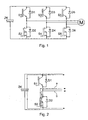
- FIG. 1 shows the basic structure of a 6-pulse inverter for driving a three-phase AC motor.
- the inverter circuitry of FIG. 1 has a total of three identical electrical half-bridges, which are fed by a DC link ZK. Each of the three half bridges has a series connection of two power switches S1 and S2, S3 and S4 or S5 and S6.
- connection of the two power switches of a half-bridge represents in each case an output of the inverter, which is connected to a motor winding of the three-phase motor M.
- the motor windings of the three-phase motor M can be arranged, for example, in star connection or triangular circuit.
- a first power switch S1, S3, S5 arranged in the form of an IGBT
- a second power switch S2, S4, S6 is arranged in the form of a MOSFET.
- the first power switches S1, S3, S5 as MOSFETs and the second power switches S2, S4, S6 may be formed as IGBTs.
- IGBTs S1, S3, S5 each have a freewheeling diode D1, D3, D5 connected in anti-parallel.
- MOSFETs S2, S4, S6 are each assigned a body diode D2, D4, D6.
- FIG. 3 is the applied from the current-voltage characteristics of a MOSFET (eg STD5N52U, curve m) and an IGBT (eg STGD6NC60HD, curve i) resulting on-resistance over the phase current.
- the resulting forward resistance results from the forward resistances of the respective circuit breaker itself and the associated diode as a function of the drain current Id or the collector current Ic.
- a first work area A with low phase currents (low power consumption) the IGBT has a significantly higher on-resistance than the MOSFET.
- the MOSFET has a higher on-resistance than the IGBT.
- the inverter has more than these two different work areas A and B.
- the first and second power switches S1-S6 are driven by a control means (not shown) so that in the first work area A, MOSFETs S2, S4, S6 are predominantly loaded, i.e., in the first working area A. are turned on and loaded in the second work area B predominantly the IGBTs S1, S3, S5, i. be turned on.
- MOSFETs S2, S4, S6 are predominantly loaded, i.e., in the first working area A. are turned on and loaded in the second work area B predominantly the IGBTs S1, S3, S5, i. be turned on.
- the power switches S1-S6 of the inverter are driven by the control device with an intermediate-circuit-clamped pulse width modulation (PWM).
- PWM pulse width modulation
- the MOSFET (e.g., S2) of one half-bridge is turned on continuously while the power switches (e.g., S3-S6) of the other half-bridges are clocked in accordance with the PWM.
- the MOSFET (eg, S4) of another half-bridge is turned on continuously, while the power switches (eg, S1-S2, S5-S6) of the remaining half-bridges are clocked, and in the next 120 ° phase, the MOSFET (eg S6) of a still other half-bridge switched on continuously while the power switches (eg S1-S6) of the remaining half-bridges are clocked.
- FIG. 2 shows by way of example the current flow through the first half-bridge of FIG. 1 during a first 120 ° phase and in the first operating range A. Since the MOSFET S2 is continuously switched on during this 120 ° phase, ie is clamped to the intermediate circuit ZK, the phase current flows both from the intermediate circuit ZK during the power consumption (current characteristic a) as well as in the freewheel (current curve b) via the MOSFET S2. Thus, during this time IGBT S1, which has a higher on-state resistance than the MOSFET S2 in the first operating region A, no forward losses occur. While this first half-bridge S1-S2 remains ungated, the two other half-bridges S3-S4 and S5-S6 are each clocked in accordance with the PWM.
- the IGBT of a half bridge is clamped onto the intermediate circuit ZK in a 120 ° phase and thus remains unclocked, while the IGBTs of the other two half-bridges are clocked according to the PWM.
- the phase currents therefore flow exclusively in the non-clocked half-bridge via the IGBTs S1, S3 and S5, respectively, which in this operating region B has a lower forward resistance than the MOSFET. In this way, the passage losses of the inverter can also be reduced in the second work area B.
- the efficiency of the inverter can be improved in this way, especially in the range of low power consumption (working area A).
Landscapes
- Engineering & Computer Science (AREA)
- Power Engineering (AREA)
- Inverter Devices (AREA)
- Direct Current Feeding And Distribution (AREA)
Applications Claiming Priority (1)
| Application Number | Priority Date | Filing Date | Title |
|---|---|---|---|
| DE102011102126A DE102011102126A1 (de) | 2011-05-20 | 2011-05-20 | Wechselrichter-Schaltungsanordnung |
Publications (3)
| Publication Number | Publication Date |
|---|---|
| EP2530824A2 true EP2530824A2 (fr) | 2012-12-05 |
| EP2530824A3 EP2530824A3 (fr) | 2017-11-22 |
| EP2530824B1 EP2530824B1 (fr) | 2021-08-18 |
Family
ID=46178392
Family Applications (1)
| Application Number | Title | Priority Date | Filing Date |
|---|---|---|---|
| EP12003822.9A Active EP2530824B1 (fr) | 2011-05-20 | 2012-05-15 | Onduleur |
Country Status (2)
| Country | Link |
|---|---|
| EP (1) | EP2530824B1 (fr) |
| DE (1) | DE102011102126A1 (fr) |
Families Citing this family (1)
| Publication number | Priority date | Publication date | Assignee | Title |
|---|---|---|---|---|
| EP4679690A1 (fr) * | 2024-07-08 | 2026-01-14 | Siemens Aktiengesellschaft | Onduleur et procédé de commande d'un onduleur |
Citations (3)
| Publication number | Priority date | Publication date | Assignee | Title |
|---|---|---|---|---|
| EP0363514A1 (fr) | 1988-10-13 | 1990-04-18 | Siemens Aktiengesellschaft | Méthode de contrôle d'un circuit utilisateur à courant triphasé par modulation d'impulsions en largeur estimant une sinusoide |
| JPH1080152A (ja) | 1996-09-06 | 1998-03-24 | Hitachi Ltd | フォークリフト用インバータ装置 |
| DE10010957A1 (de) | 2000-03-06 | 2001-09-13 | Still Gmbh | Leistungsschalter für Drei-Phasen-Umrichter |
Family Cites Families (4)
| Publication number | Priority date | Publication date | Assignee | Title |
|---|---|---|---|---|
| US5107151A (en) * | 1989-08-22 | 1992-04-21 | Unique Mobility, Inc. | Switching circuit employing electronic devices in series with an inductor to avoid commutation breakdown and extending the current range of switching circuits by using igbt devices in place of mosfets |
| JP4942967B2 (ja) * | 2005-09-08 | 2012-05-30 | 東芝キヤリア株式会社 | インバータ装置及び冷凍サイクル装置 |
| US7679310B2 (en) * | 2007-10-24 | 2010-03-16 | Gm Global Technology Operations, Inc. | Method and system for controlling pulse width modulation in a power inverter in electric drives |
| JP2010088191A (ja) * | 2008-09-30 | 2010-04-15 | Sharp Corp | インバータ装置 |
-
2011
- 2011-05-20 DE DE102011102126A patent/DE102011102126A1/de not_active Withdrawn
-
2012
- 2012-05-15 EP EP12003822.9A patent/EP2530824B1/fr active Active
Patent Citations (3)
| Publication number | Priority date | Publication date | Assignee | Title |
|---|---|---|---|---|
| EP0363514A1 (fr) | 1988-10-13 | 1990-04-18 | Siemens Aktiengesellschaft | Méthode de contrôle d'un circuit utilisateur à courant triphasé par modulation d'impulsions en largeur estimant une sinusoide |
| JPH1080152A (ja) | 1996-09-06 | 1998-03-24 | Hitachi Ltd | フォークリフト用インバータ装置 |
| DE10010957A1 (de) | 2000-03-06 | 2001-09-13 | Still Gmbh | Leistungsschalter für Drei-Phasen-Umrichter |
Also Published As
| Publication number | Publication date |
|---|---|
| DE102011102126A1 (de) | 2012-11-22 |
| EP2530824B1 (fr) | 2021-08-18 |
| EP2530824A3 (fr) | 2017-11-22 |
Similar Documents
| Publication | Publication Date | Title |
|---|---|---|
| EP3503365B1 (fr) | Procédé et dispositif de commande de modules de commutation mos à effet de champ | |
| DE102015214768A1 (de) | Steuervorrichtung für eine rotationsmaschine | |
| DE102011014165A1 (de) | Umrichter für eine elektrische Maschine und Verfahren zur Ansteuerung eines Leistungsschalters | |
| DE112018006822T5 (de) | Leistungsumwandlungsvorrichtung, motormodul und elektrische servolenkvorrichtung | |
| DE10010957A1 (de) | Leistungsschalter für Drei-Phasen-Umrichter | |
| DE102017115639A1 (de) | Reduzierung des Rippelstroms bei Schaltvorgängen einer Brückenschaltung | |
| EP1936789B1 (fr) | Circuit de delai pour un convertisseur MLI | |
| DE102016215175B4 (de) | Verfahren zum Betreiben einer elektrischen Maschine und elektrische Maschine | |
| EP3251194B1 (fr) | Ensemble d'accumulation d'énergie | |
| EP3652849B1 (fr) | Couplage de circuit intermédiaire dans des groupes d'entraînement | |
| DE102013213045A1 (de) | Vermeidung von Bremsmomenten bei permanenterregten Synchronmaschinen | |
| DE102011081215A1 (de) | Drehstrommaschinen-Ansteuerungsverfahren und -vorrichtung | |
| EP2530824B1 (fr) | Onduleur | |
| DE102021003587A1 (de) | Verfahren zum Betrieb eines batterieelektrischen Fahrzeugs | |
| DE102021105185A1 (de) | Umrichter, Kraftfahrzeug und Verfahren zur Steuerung einer Halbbrückenschaltung | |
| DE102004042256A1 (de) | Gleichspannungszwischenkreis | |
| DE102008019294A1 (de) | Versorgungseinheit für elektrische Antriebe und Verfahren zur Steuerung dieser Versorgungseinheit | |
| DE102020215370B4 (de) | Fahrzeugbetrieb-Inverter, Fahrzeugantrieb und Verfahren zum Betreiben eines Fahrzeugantrieb-Inverters | |
| DE102021214531A1 (de) | Verfahren zur Ansteuerung einer Schaltungsanordnung für Leistungshalbleiter | |
| DE102013218799A1 (de) | Modularer Stromrichter | |
| DE102011083841A1 (de) | Verfahren und Vorrichtung zur Ansteuerung eines abschaltbaren Leistungshalbleiterschalters | |
| DE102008049536B3 (de) | Kreisstromunterdrückende Ansteuerung bei einer Gleichrichterschaltung | |
| EP2536019B1 (fr) | Procédé destiné à la commande d'un convertisseur | |
| DE102022211580B4 (de) | Verfahren zur Ansteuerung von topologischen Schaltern einer Halbbrücke in einem Leistungsmodul eines Inverters | |
| DE102024133664B3 (de) | Traktionsnetz für ein Elektrofahrzeug |
Legal Events
| Date | Code | Title | Description |
|---|---|---|---|
| PUAI | Public reference made under article 153(3) epc to a published international application that has entered the european phase |
Free format text: ORIGINAL CODE: 0009012 |
|
| AK | Designated contracting states |
Kind code of ref document: A2 Designated state(s): AL AT BE BG CH CY CZ DE DK EE ES FI FR GB GR HR HU IE IS IT LI LT LU LV MC MK MT NL NO PL PT RO RS SE SI SK SM TR |
|
| AX | Request for extension of the european patent |
Extension state: BA ME |
|
| PUAL | Search report despatched |
Free format text: ORIGINAL CODE: 0009013 |
|
| AK | Designated contracting states |
Kind code of ref document: A3 Designated state(s): AL AT BE BG CH CY CZ DE DK EE ES FI FR GB GR HR HU IE IS IT LI LT LU LV MC MK MT NL NO PL PT RO RS SE SI SK SM TR |
|
| AX | Request for extension of the european patent |
Extension state: BA ME |
|
| RIC1 | Information provided on ipc code assigned before grant |
Ipc: H02M 7/5387 20070101AFI20171018BHEP |
|
| STAA | Information on the status of an ep patent application or granted ep patent |
Free format text: STATUS: REQUEST FOR EXAMINATION WAS MADE |
|
| 17P | Request for examination filed |
Effective date: 20180314 |
|
| RBV | Designated contracting states (corrected) |
Designated state(s): AL AT BE BG CH CY CZ DE DK EE ES FI FR GB GR HR HU IE IS IT LI LT LU LV MC MK MT NL NO PL PT RO RS SE SI SK SM TR |
|
| STAA | Information on the status of an ep patent application or granted ep patent |
Free format text: STATUS: EXAMINATION IS IN PROGRESS |
|
| 17Q | First examination report despatched |
Effective date: 20200730 |
|
| GRAP | Despatch of communication of intention to grant a patent |
Free format text: ORIGINAL CODE: EPIDOSNIGR1 |
|
| STAA | Information on the status of an ep patent application or granted ep patent |
Free format text: STATUS: GRANT OF PATENT IS INTENDED |
|
| INTG | Intention to grant announced |
Effective date: 20210203 |
|
| GRAS | Grant fee paid |
Free format text: ORIGINAL CODE: EPIDOSNIGR3 |
|
| GRAA | (expected) grant |
Free format text: ORIGINAL CODE: 0009210 |
|
| STAA | Information on the status of an ep patent application or granted ep patent |
Free format text: STATUS: THE PATENT HAS BEEN GRANTED |
|
| AK | Designated contracting states |
Kind code of ref document: B1 Designated state(s): AL AT BE BG CH CY CZ DE DK EE ES FI FR GB GR HR HU IE IS IT LI LT LU LV MC MK MT NL NO PL PT RO RS SE SI SK SM TR |
|
| REG | Reference to a national code |
Ref country code: GB Ref legal event code: FG4D Free format text: NOT ENGLISH |
|
| REG | Reference to a national code |
Ref country code: CH Ref legal event code: EP |
|
| REG | Reference to a national code |
Ref country code: DE Ref legal event code: R096 Ref document number: 502012016873 Country of ref document: DE |
|
| REG | Reference to a national code |
Ref country code: IE Ref legal event code: FG4D Free format text: LANGUAGE OF EP DOCUMENT: GERMAN Ref country code: AT Ref legal event code: REF Ref document number: 1422535 Country of ref document: AT Kind code of ref document: T Effective date: 20210915 |
|
| REG | Reference to a national code |
Ref country code: LT Ref legal event code: MG9D |
|
| REG | Reference to a national code |
Ref country code: NL Ref legal event code: MP Effective date: 20210818 |
|
| PG25 | Lapsed in a contracting state [announced via postgrant information from national office to epo] |
Ref country code: LT Free format text: LAPSE BECAUSE OF FAILURE TO SUBMIT A TRANSLATION OF THE DESCRIPTION OR TO PAY THE FEE WITHIN THE PRESCRIBED TIME-LIMIT Effective date: 20210818 Ref country code: BG Free format text: LAPSE BECAUSE OF FAILURE TO SUBMIT A TRANSLATION OF THE DESCRIPTION OR TO PAY THE FEE WITHIN THE PRESCRIBED TIME-LIMIT Effective date: 20211118 Ref country code: PT Free format text: LAPSE BECAUSE OF FAILURE TO SUBMIT A TRANSLATION OF THE DESCRIPTION OR TO PAY THE FEE WITHIN THE PRESCRIBED TIME-LIMIT Effective date: 20211220 Ref country code: RS Free format text: LAPSE BECAUSE OF FAILURE TO SUBMIT A TRANSLATION OF THE DESCRIPTION OR TO PAY THE FEE WITHIN THE PRESCRIBED TIME-LIMIT Effective date: 20210818 Ref country code: NO Free format text: LAPSE BECAUSE OF FAILURE TO SUBMIT A TRANSLATION OF THE DESCRIPTION OR TO PAY THE FEE WITHIN THE PRESCRIBED TIME-LIMIT Effective date: 20211118 Ref country code: FI Free format text: LAPSE BECAUSE OF FAILURE TO SUBMIT A TRANSLATION OF THE DESCRIPTION OR TO PAY THE FEE WITHIN THE PRESCRIBED TIME-LIMIT Effective date: 20210818 Ref country code: ES Free format text: LAPSE BECAUSE OF FAILURE TO SUBMIT A TRANSLATION OF THE DESCRIPTION OR TO PAY THE FEE WITHIN THE PRESCRIBED TIME-LIMIT Effective date: 20210818 Ref country code: HR Free format text: LAPSE BECAUSE OF FAILURE TO SUBMIT A TRANSLATION OF THE DESCRIPTION OR TO PAY THE FEE WITHIN THE PRESCRIBED TIME-LIMIT Effective date: 20210818 Ref country code: SE Free format text: LAPSE BECAUSE OF FAILURE TO SUBMIT A TRANSLATION OF THE DESCRIPTION OR TO PAY THE FEE WITHIN THE PRESCRIBED TIME-LIMIT Effective date: 20210818 |
|
| PG25 | Lapsed in a contracting state [announced via postgrant information from national office to epo] |
Ref country code: PL Free format text: LAPSE BECAUSE OF FAILURE TO SUBMIT A TRANSLATION OF THE DESCRIPTION OR TO PAY THE FEE WITHIN THE PRESCRIBED TIME-LIMIT Effective date: 20210818 Ref country code: LV Free format text: LAPSE BECAUSE OF FAILURE TO SUBMIT A TRANSLATION OF THE DESCRIPTION OR TO PAY THE FEE WITHIN THE PRESCRIBED TIME-LIMIT Effective date: 20210818 Ref country code: GR Free format text: LAPSE BECAUSE OF FAILURE TO SUBMIT A TRANSLATION OF THE DESCRIPTION OR TO PAY THE FEE WITHIN THE PRESCRIBED TIME-LIMIT Effective date: 20211119 |
|
| PG25 | Lapsed in a contracting state [announced via postgrant information from national office to epo] |
Ref country code: NL Free format text: LAPSE BECAUSE OF FAILURE TO SUBMIT A TRANSLATION OF THE DESCRIPTION OR TO PAY THE FEE WITHIN THE PRESCRIBED TIME-LIMIT Effective date: 20210818 |
|
| PG25 | Lapsed in a contracting state [announced via postgrant information from national office to epo] |
Ref country code: DK Free format text: LAPSE BECAUSE OF FAILURE TO SUBMIT A TRANSLATION OF THE DESCRIPTION OR TO PAY THE FEE WITHIN THE PRESCRIBED TIME-LIMIT Effective date: 20210818 |
|
| REG | Reference to a national code |
Ref country code: DE Ref legal event code: R097 Ref document number: 502012016873 Country of ref document: DE |
|
| PG25 | Lapsed in a contracting state [announced via postgrant information from national office to epo] |
Ref country code: SM Free format text: LAPSE BECAUSE OF FAILURE TO SUBMIT A TRANSLATION OF THE DESCRIPTION OR TO PAY THE FEE WITHIN THE PRESCRIBED TIME-LIMIT Effective date: 20210818 Ref country code: SK Free format text: LAPSE BECAUSE OF FAILURE TO SUBMIT A TRANSLATION OF THE DESCRIPTION OR TO PAY THE FEE WITHIN THE PRESCRIBED TIME-LIMIT Effective date: 20210818 Ref country code: RO Free format text: LAPSE BECAUSE OF FAILURE TO SUBMIT A TRANSLATION OF THE DESCRIPTION OR TO PAY THE FEE WITHIN THE PRESCRIBED TIME-LIMIT Effective date: 20210818 Ref country code: EE Free format text: LAPSE BECAUSE OF FAILURE TO SUBMIT A TRANSLATION OF THE DESCRIPTION OR TO PAY THE FEE WITHIN THE PRESCRIBED TIME-LIMIT Effective date: 20210818 Ref country code: CZ Free format text: LAPSE BECAUSE OF FAILURE TO SUBMIT A TRANSLATION OF THE DESCRIPTION OR TO PAY THE FEE WITHIN THE PRESCRIBED TIME-LIMIT Effective date: 20210818 Ref country code: AL Free format text: LAPSE BECAUSE OF FAILURE TO SUBMIT A TRANSLATION OF THE DESCRIPTION OR TO PAY THE FEE WITHIN THE PRESCRIBED TIME-LIMIT Effective date: 20210818 |
|
| PLBE | No opposition filed within time limit |
Free format text: ORIGINAL CODE: 0009261 |
|
| STAA | Information on the status of an ep patent application or granted ep patent |
Free format text: STATUS: NO OPPOSITION FILED WITHIN TIME LIMIT |
|
| 26N | No opposition filed |
Effective date: 20220519 |
|
| PG25 | Lapsed in a contracting state [announced via postgrant information from national office to epo] |
Ref country code: IT Free format text: LAPSE BECAUSE OF FAILURE TO SUBMIT A TRANSLATION OF THE DESCRIPTION OR TO PAY THE FEE WITHIN THE PRESCRIBED TIME-LIMIT Effective date: 20210818 |
|
| PG25 | Lapsed in a contracting state [announced via postgrant information from national office to epo] |
Ref country code: SI Free format text: LAPSE BECAUSE OF FAILURE TO SUBMIT A TRANSLATION OF THE DESCRIPTION OR TO PAY THE FEE WITHIN THE PRESCRIBED TIME-LIMIT Effective date: 20210818 |
|
| PGFP | Annual fee paid to national office [announced via postgrant information from national office to epo] |
Ref country code: DE Payment date: 20220720 Year of fee payment: 11 |
|
| REG | Reference to a national code |
Ref country code: CH Ref legal event code: PL |
|
| REG | Reference to a national code |
Ref country code: BE Ref legal event code: MM Effective date: 20220531 |
|
| GBPC | Gb: european patent ceased through non-payment of renewal fee |
Effective date: 20220515 |
|
| PG25 | Lapsed in a contracting state [announced via postgrant information from national office to epo] |
Ref country code: MC Free format text: LAPSE BECAUSE OF FAILURE TO SUBMIT A TRANSLATION OF THE DESCRIPTION OR TO PAY THE FEE WITHIN THE PRESCRIBED TIME-LIMIT Effective date: 20210818 Ref country code: LU Free format text: LAPSE BECAUSE OF NON-PAYMENT OF DUE FEES Effective date: 20220515 Ref country code: LI Free format text: LAPSE BECAUSE OF NON-PAYMENT OF DUE FEES Effective date: 20220531 Ref country code: CH Free format text: LAPSE BECAUSE OF NON-PAYMENT OF DUE FEES Effective date: 20220531 |
|
| PG25 | Lapsed in a contracting state [announced via postgrant information from national office to epo] |
Ref country code: IE Free format text: LAPSE BECAUSE OF NON-PAYMENT OF DUE FEES Effective date: 20220515 Ref country code: FR Free format text: LAPSE BECAUSE OF NON-PAYMENT OF DUE FEES Effective date: 20220531 |
|
| PG25 | Lapsed in a contracting state [announced via postgrant information from national office to epo] |
Ref country code: GB Free format text: LAPSE BECAUSE OF NON-PAYMENT OF DUE FEES Effective date: 20220515 Ref country code: BE Free format text: LAPSE BECAUSE OF NON-PAYMENT OF DUE FEES Effective date: 20220531 |
|
| REG | Reference to a national code |
Ref country code: AT Ref legal event code: MM01 Ref document number: 1422535 Country of ref document: AT Kind code of ref document: T Effective date: 20220515 |
|
| PG25 | Lapsed in a contracting state [announced via postgrant information from national office to epo] |
Ref country code: AT Free format text: LAPSE BECAUSE OF NON-PAYMENT OF DUE FEES Effective date: 20220515 |
|
| REG | Reference to a national code |
Ref country code: DE Ref legal event code: R119 Ref document number: 502012016873 Country of ref document: DE |
|
| PG25 | Lapsed in a contracting state [announced via postgrant information from national office to epo] |
Ref country code: HU Free format text: LAPSE BECAUSE OF FAILURE TO SUBMIT A TRANSLATION OF THE DESCRIPTION OR TO PAY THE FEE WITHIN THE PRESCRIBED TIME-LIMIT; INVALID AB INITIO Effective date: 20120515 |
|
| PG25 | Lapsed in a contracting state [announced via postgrant information from national office to epo] |
Ref country code: MK Free format text: LAPSE BECAUSE OF FAILURE TO SUBMIT A TRANSLATION OF THE DESCRIPTION OR TO PAY THE FEE WITHIN THE PRESCRIBED TIME-LIMIT Effective date: 20210818 Ref country code: DE Free format text: LAPSE BECAUSE OF NON-PAYMENT OF DUE FEES Effective date: 20231201 Ref country code: CY Free format text: LAPSE BECAUSE OF FAILURE TO SUBMIT A TRANSLATION OF THE DESCRIPTION OR TO PAY THE FEE WITHIN THE PRESCRIBED TIME-LIMIT Effective date: 20210818 |
|
| PG25 | Lapsed in a contracting state [announced via postgrant information from national office to epo] |
Ref country code: TR Free format text: LAPSE BECAUSE OF FAILURE TO SUBMIT A TRANSLATION OF THE DESCRIPTION OR TO PAY THE FEE WITHIN THE PRESCRIBED TIME-LIMIT Effective date: 20210818 |
|
| PG25 | Lapsed in a contracting state [announced via postgrant information from national office to epo] |
Ref country code: MT Free format text: LAPSE BECAUSE OF FAILURE TO SUBMIT A TRANSLATION OF THE DESCRIPTION OR TO PAY THE FEE WITHIN THE PRESCRIBED TIME-LIMIT Effective date: 20210818 |