EP2533286A2 - Integrierte Halbleiterschaltung mit Speicherzellen - Google Patents
Integrierte Halbleiterschaltung mit Speicherzellen Download PDFInfo
- Publication number
- EP2533286A2 EP2533286A2 EP12167829A EP12167829A EP2533286A2 EP 2533286 A2 EP2533286 A2 EP 2533286A2 EP 12167829 A EP12167829 A EP 12167829A EP 12167829 A EP12167829 A EP 12167829A EP 2533286 A2 EP2533286 A2 EP 2533286A2
- Authority
- EP
- European Patent Office
- Prior art keywords
- well
- cell
- memory cells
- placement
- wells
- Prior art date
- Legal status (The legal status is an assumption and is not a legal conclusion. Google has not performed a legal analysis and makes no representation as to the accuracy of the status listed.)
- Granted
Links
Images


Classifications
-
- H—ELECTRICITY
- H10—SEMICONDUCTOR DEVICES; ELECTRIC SOLID-STATE DEVICES NOT OTHERWISE PROVIDED FOR
- H10D—INORGANIC ELECTRIC SEMICONDUCTOR DEVICES
- H10D84/00—Integrated devices formed in or on semiconductor substrates that comprise only semiconducting layers, e.g. on Si wafers or on GaAs-on-Si wafers
- H10D84/90—Masterslice integrated circuits
- H10D84/903—Masterslice integrated circuits comprising field effect technology
- H10D84/907—CMOS gate arrays
-
- H—ELECTRICITY
- H10—SEMICONDUCTOR DEVICES; ELECTRIC SOLID-STATE DEVICES NOT OTHERWISE PROVIDED FOR
- H10D—INORGANIC ELECTRIC SEMICONDUCTOR DEVICES
- H10D89/00—Aspects of integrated devices not covered by groups H10D84/00 - H10D88/00
- H10D89/10—Integrated device layouts
Definitions
- the disclosures herein relate to cell placement, a semiconductor circuit, and a method of placing circuit element cells.
- LSI large-scale integrated circuit
- Logic cells prepared in advance are called standard cells, which may include basic circuit gates and more complex logic circuits such as flip flops.
- Cells incorporated in cell-based design may also include macro-cells or the like defining larger-scale circuits such as a ROM, a RAM, and an AD converter.
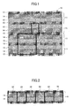
- Fig. 1 is a drawing illustrating a standard-cell-placement area used in cell-based design.
- Vdd lines 12 for supplying a power supply potential Vdd and Gnd lines 13 for supplying a ground potential Gnd are arranged alternately at constant intervals.
- An area between a Vdd line 12 and an adjacent Gnd line 13 constitutes a cell-placement row 11 having a constant height (and width).
- Each cell-placement row 11 has an N well 14 and a P well 15 formed therein that extend in the same direction as the direction in which the cell-placement row 11 extends.
- the N well 14 is electrically connected to the corresponding Vdd line 12 through a contact
- the P well 15 is electrically connected to the corresponding Gnd line 13 through a contact.
- a standard cell 16 has the same height as the cell-placement row 11, and a standard cell 17 has a height twice as large as the cell-placement row 11.
- the height of a standard cell is restricted to the same height as the cell-placement row 11 or an integer multiple of the height of the cell-placement row 11. This ensures that an orderly cell arrangement is naturally obtained upon placing a plurality of standard cells, thereby simplifying the task of placing cells.
- a general standard cell includes one or more P-channel-type transistors (i.e., PMOS transistors) and one or more N-channel-type transistors (i.e., NMOS transistors).
- PMOS transistors are formed in the N well 14, and NMOS transistors are formed in the P well 15.
- the N well 14 is connected to the corresponding Vdd line 12. Because of this, it is preferable for the N well 14 to extend along and in parallel to the Vdd line 12 (i.e., in parallel to the cell-placement row 11).
- the P well 15 is conneced to the corresponding Gnd line 13.
- the P well 15 it is preferable for the P well 15 to extend along and in parallel to the Gnd line 13 (i.e., in parallel to the cell-placement row 11). Further, with a premise that the N well 14 and the P well 15 are formed in parallel to the cell-placement row 11 as illustrated in Fig. 1 , a standard cell that is designed based upon this premise can be placed anywhere in the cell-placement row 11 without modifying the design of the wells. In this manner, a standard cell is typically designed based upon a premise that the N well 14 and the P well 15 are formed in parallel to the cell-placement row 11 as illustrated in Fig. 1 .
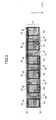
- Fig. 2 is a drawing illustrating a configuration in which a plurality of latches for storing a plurality of bits are arranged in line on the cell-placement row.
- six latches 20, each of which is a standard cell are arranged in the cell-placement row 11 without having any gaps therebetween.
- the six latches 20 can store 6 bit data.
- One of the six latches 20 may store a parity bit that is generated from the 5-bit data stored in the five remaining latches 20.
- Nine latches 20 may be arranged instead of six latches. Such nine latches can store one-byte data and one parity bit.
- a critical charge amount i.e., the amount of electric charge needed to invert stored data
- a critical charge amount decreases because of reduction in the power supply voltage and internal capacitance of a memory element such as a latch. This results in an increase in the probability of soft error by which stored data is inverted due to an arrival of ⁇ ray or neutron ray. Entry of ⁇ ray into an N well or P well, for example, results in a large number of electron-hole pairs being generated in the well. These electron-hole pairs are then scattered in every direction within the well. Electrons generated by an arrival of ⁇ ray into an N well tend to be collected by Vdd since the N well is coupled to the power supply potential Vdd.
- electrons are the majority carrier in the N well. Because of this, these electrons have little effect on P-type diffusion regions existing in the N well. Holes generated together with these electrons, however, end up changing the potential of the P-type diffusion regions existing in the N well upon being collected by these regions. Especially when the P-type diffusion regions are coupled to the ground voltage Gnd, the above-noted change occurs as a change toward higher potentials, thereby causing soft error. Holes generated by an arrival of ⁇ ray into a P well tend to be collected by Gnd since the P well is coupled to the ground potential Gnd. Also, holes are the majority carrier in the P well. Because of this, these holes have little effect on N-type diffusion regions existing in the P well.
- Electrons generated together with these holes end up changing the potential of the N-type diffusion regions existing in the P well upon being collected by these regions. Especially when the N-type diffusion regions are coupled to the ground voltage Gnd, the above-noted change occurs as a change toward lower potentials, thereby causing soft error.
- the mechanism for correcting error by use of error correction code can detect two-bit errors, but cannot correct these errors. Moreover, errors occurring with respect to three or more bits cannot be correctly detected even by use of error correction codes. Occurrence of errors in a plurality of bits may thus result in a performance drop due to a need for an extra action such as an instruction retry, or may result in a failure to perform correct circuit operations.
- Measures for preventing soft error may be taken as follows.
- the number of transistors may be increased and a new latch structure may be devised such as in the case of DICE (i.e., Dual Interlocked Storage Cell), for example, thereby increasing a tolerance level of a latch against soft error.
- the size of transistors in a latch may be increased to increase the critical charge amount, thereby increasing a tolerance level of the latch against soft error.
- the distance between adjacent latches for storing adjacent bits may be increased to reduce the possibility of electrons reaching the adjacent bit upon being generated by an arrival of ⁇ ray.
- a dummy P-well region (or N-well region) may be provided on a memory-cell border in the common N-type well region (or P-type well region) shared by adjacent memory cells as disclosed in Patent Document 1, thereby reducing soft error.
- Devising a latch structure such as a DICE latch or increasing a critical charge amount by enlarging transistor size give rise to a problem in that power consumption and circuit size significantly increase.
- an increase in the soft-error tolerance of a latch does not completely remove the possibility of soft error. When error occurs, therefore, plural bits may suffer errors if a common well region is used as in the previously-described cell-based design.
- An increase in the distance between adjacent latches for storing adjacent bits also gives rise to a problem of a size increase. If the distance is not sufficiently increased due to consideration to the problem of a size increase, the possibility of plural bit errors is not sufficiently lowered.
- N wells and P wells end up being arranged in a checkerboard pattern. Namely, dummy P-well regions are inserted into the N well 14 between adjacent latches 20 illustrated in Fig. 2 , and, also, dummy N-well regions are inserted into the P well 15 between adjacent latches 20, so that the dummy P-well regions and the dummy N-well regions are opposed to each other.
- Each dummy well region is isolated, and needs to satisfy the minimum size requirement of a well as defined by the process used. This requirement causes the size of a dummy well region to be relatively large.
- each well region is isolated also gives rise to a problem in that an area for coupling each well to the corresponding potential may need to be newly provided. Moreover, an actual process involves manufacturing error. Because of this, the same-conduction-type wells may be connected to each other in a diagonal direction at the corners of wells. It may thus be the case that the wells cannot be completely separated from each other between adjacent latches 20.
- a semiconductor integrated circuit includes a plurality of memory cells arranged in a cell-placement row extending in a first direction, a first N well and a first P well arranged in a second direction perpendicular to the first direction in each area of the memory cells, and a second N well and a second P well each having the same length as a width of the cell-placement row and situated between at least two adjacent memory cells of the plurality of memory cells, wherein the first N well and the second N well are integrated, and the first P well and the second P well are integrated.
- a semiconductor integrated circuit includes a plurality of memory elements arranged in a cell-placement row extending in a first direction and formed in a first N well and a first P well arranged in a second direction perpendicular to the first direction, and a second N well and a second P well each having the same length as a width of the cell-placement row and situated between at least two adjacent memory elements of the plurality of memory elements, wherein the first N well and the second N well are integrated, and the first P well and the second P well are integrated, and wherein the plurality of memory elements store respective bits of one data item.
- a method of placing circuit element cells by use of a computer includes placing a plurality of memory cells in a cell-placement row extending in a first direction, the plurality of memory cells being formed in a first N well and a first P well arranged in a second direction perpendicular to the first direction, and placing, between at least two adjacent memory cells of the plurality of memory cells, a cell including a second N well and a second P well each having the same length as a width of the cell-placement row.
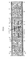
- Fig. 3 is a drawing illustrating an example of the placement structure of circuit element cells.
- a plurality of memory cells 30 are arranged in a cell-placement row 31 that extends in a first direction (i.e., X direction in Fig. 3 ).
- the cell-placement row 31 is an area between a Vdd line 32 and a Gnd line 33, and has a constant height (and width).
- a first N well 34 and a first P well 35 are arranged in a second direction (i.e., Y direction in Fig.
- a second N well 36 and a second P well 37 each having the same length as the width of the cell-placement row 31 are inserted.
- the first N well 34 and the second N well 36 illustrated as being adjacent to each other constitute an integrated, unitary, continuous well region.
- the first P well 35 and the second P well 37 illustrated as being adjacent to each other constitute an integrated, unitary, continuous well region.
- Each of the N well 36 and the P well 37 may have a slit shape having a length in the Y direction that is substantially longer than its width in the X direction.
- the N well 36 and the P well 37 forming a pair are arranged in such a positional relationship that the N well 36 is situated to the left-hand side of the figure and the P well 37 is situated to the right-hand side of the figure.
- the arrangement of the N well 36 and the P well 37 is not limited to this example.
- the N well 36 and the P well 37 forming a pair are arranged in such a positional relationship that the N well 36 is situated to the right-hand side of the figure and the P well 37 is situated to the left-hand side of the figure.
- the N well 36 and the P well 37 forming a pair arranged in such a positional relationship that the N well 36 is situated to the left-hand side of the figure and the P well 37 is situated to the right-hand side of the figure may be used together with the N well 36 and the P well 37 forming a pair arranged in such a positional relationship that the N well 36 is situated to the right-hand side of the figure and the P well 37 is situated to the left-hand side of the figure.
- the N well 36 may have a potential contact part for coupling the N well 34 and 36 to the Vdd potential.
- the P well 37 may have a potential contact part for coupling the P well 35 and 37 to the Gnd potential.
- the memory cells 30 may store respective bits which constitute a single data item.
- Data stored in at least one of the memory cells 30 may be a value obtained from the data stored in the remaining memory cells 30.
- one bit stored in one of the memory cells 30 may be a parity bit obtained from the five bits stored in the five remaining memory cells 30.
- one or more bits stored in at least one of the memory cells 30 may be one or more redundant bits for error correction obtained from the bits stored in the remaining memory cells 30.
- the wells of adjacent memory cells 30 are separated from each other by a well of a different conduction type. Namely, the N wells 34 of adjacent memory cells 30 are separated from each other by the P well 37. Also, the P wells 35 of adjacent memory cells 30 are separated from each other by the N well 36. With this structure, wells are isolated from each other between adjacent memory cells 30, making it difficult for soft error to propagate to an adjacent bit.
- the P well 35 and 37 is coupled to the ground potential Gnd
- the N well 34 and 36 is coupled to the power supply potential Vdd, so that they are placed in a reverse bias condition.
- the N well 36 is continuous with the N well 34
- the P well 37 is continuous with the P well 35. Because of this, the N well 36 or the P well 37 alone does not have to satisfy the minimum size requirement of a well. It suffices for the combined N well 34 and 36 or the combined P well 35 and 37 as a whole to satisfy the minimum size requirement of a well. The size of the N well 36 and the P well 37 can thus be reduced. Further, there is no point at which corners of wells of the same conduction type meet each other as in the case of a checkerboard pattern. This can avoid unintentional coupling between wells that are supposed to be separated from each other.
- the N well 34 and the P well 35 are arranged in the width direction of the cell placement row (i.e., in the Y direction) as in the case of the standard placement area used in cell-based design illustrated in Fig. 1 .
- standard cells having the same design as conventional standard cells used in the cell-based design illustrated in Fig. 1 can be used to design the cell placement structure illustrated in Fig. 3 according to cell-based design.
- the design of existing standard cells can be used without any modification, thereby achieving utilization of existing resources, for the purpose of suppressing soft errors occurring in a plurality of bits.
- FIG. 4 is a drawing illustrating an example of the circuit configuration of a latch serving as a memory cell 30.
- a latch illustrated in Fig. 4 includes PMOS transistors 41 through 46 and NMOS transistors 47 through 52.
- An inverter including the PMOS transistor 44 and the NMOS transistor 50 and an inverter including the PMOS transistor 46 and the NMOS transistor 52 are connected to each other such that the output of any given inverter is coupled to the input of the other inverter, thereby forming a latch circuit.
- a transmission gate including the PMOS transistor 43 and the NMOS transistor 49 is opened and closed.
- data applied to a data terminal D is latched by the above-noted latch circuit.
- the data latched by the latch circuit is output from an output terminal X through an output driver including the PMOS transistor 45 and the NMOS transistor 51.
- Fig. 5 is a drawing illustrating an example of the layout of a semiconductor integrated circuit implemented by use of the cell placement structure illustrated in Fig. 3 and the latch circuit configuration illustrated in Fig. 4 .
- the same or corresponding elements as those of Fig. 3 are referred to by the same or corresponding numerals, and a description thereof will be omitted as appropriate.
- the six memory cells (latches) 30 are arranged in line, with the N well 36 and the P well 37 inserted between adjacent latches 30.
- Fig. 6 is a drawing providing an enlarged view of three consecutive latches 30 among the memory cells 30 illustrated in Fig. 5 .
- the latches 30 are arranged in line, with the N well 36 and the P well 37 inserted between adjacent latches 30.
- Each latch 30 is formed on the N well 34 and the P well 35.
- a P-type diffusion region 61 formed in the N well 34 is coupled to the Vdd line 32 through a contact 62 and a metal line 63.
- This P-type diffusion region 61 corresponds to the Vdd-side diffusion region of the PMOS transistor 42 illustrated in Fig. 4 .
- an N-type diffusion region 64 formed in the P well 35 is coupled to the Gnd line 33 through a contact 65 and a metal line 66.
- This N-type diffusion region 64 corresponds to the Gnd-side diffusion region of the NMOS transistor 48 illustrated in Fig. 4 .
- Fig. 7 is a drawing illustrating an example of the configuration of a plurality of cell-placement rows to which the cell placement structure illustrated in Fig. 3 is applied.
- Vdd lines 32 extending in the X direction for supplying the power supply potential Vdd
- Gnd lines 33 extending in the X direction for supplying the ground potential Gnd are arranged alternately in the Y direction at constant intervals.
- Areas between the Vdd lines 32 and the Gnd lines 33 constitute cell-placement rows 31-1 through 31-3 having a constant height (and width). Namely, the three cell-placement rows 31-1 through 31-3 are disposed side by side in the Y direction.
- each of the cell-placement rows 31-1 through 31-3 extending in the X direction has a plurality of memory cells 30 arranged therein.
- an N well and a P well are arranged in the Y direction.
- a N well 36 and a P well 37 each having the same length as the width of the cell-placement row are inserted.
- the memory cells 30 provided in the cell-placement row 31-1 store respective bits (which may include a parity bit or one or more redundant bits) of one data item.
- the memory cells 30 provided in the cell-placement row 31-2 store respective bits (which may include a parity bit or one or more redundant bits) of another data item.
- the memory cells 30 provided in the cell-placement row 31-3 store respective bits (which may include a parity bit or one or more redundant bits) of yet another data item.
- the positions in the X-direction of the N wells 36 and the P wells 37 are aligned between different cell-placement rows.
- the N wells 36 and the P wells 37 hold the same positions in the X direction in the cell-placement rows 31-1 through 31-3.
- the N wells 36 and the P wells 37 provided in the cell-placement row 31-1 are integral and continuous with the N wells 36 and the P wells 37, respectively, provided in the cell-placement row 31-2, and are further integral and continuous with the N wells 36 and the P wells 37, respectively, provided in the cell-placement row 31-3. This serves to simplify the structure of wells.
- the N wells 36 and the P wells 37 are continuous in the Y direction across the three cell-placement rows 31-1 through 31-3, it may be possible that soft error generated in a given cell-placement row travels to another cell-placement row. Namely, the occurrence of soft error in one memory cell 30 of the cell-placement row 31-1 may be accompanied the occurrence of soft error in the memory cells 30 in the same X direction in the remaining cell-placement rows 31-2 and 31-3. However, only 1-bit soft error occurs in the plurality of bits of a single cell-placement row that stores one data item, so that such an error can be properly dealt with by a parity check or error correction.
- Fig. 8 is a drawing illustrating a variation of the configuration of the cell-placement structure.
- the same or corresponding elements as those of Fig. 3 are referred to by the same or corresponding numerals, and a description thereof will be omitted as appropriate.
- an N well 36 and a P well 37 each having the same length as the width of the cell-placement row 31 are inserted.
- the N wells 34 and the N well 36 illustrated as being adjacent to each other constitute an integrated, unitary, continuous well region.
- the P wells 35 and the P well 37 illustrated as being adjacent to each other constitute an integrated, unitary, continuous well region.
- pairs of N wells 36 and P wells 37 are situated at intervals of two or more memory cells 30, which differs from the configuration illustrated in Fig. 3 .
- pairs of N wells 36 and P wells 37 are situated at intervals of two memory cells 30.
- Two adjacent memory cells 30 between which a pair of an N well 36 and a P well 37 is not situated have a continuous N well 34 and a continuous P well 35.
- a mechanism for detecting or correcting errors up to two bits may be employed. In such a case, soft error can be properly dealt with even if every two bits of memory cells 30 are put together, with isolations being provided at intervals of two bits as illustrated in Fig. 8 .
- This configuration allows the number of N wells 36 and P wells 37 to be reduced, thereby reducing the circuit area size.
- Fig. 9 is a drawing illustrating an example of the placement of potential contact parts for wells in the cell-placement structure.
- the same or corresponding elements as those of Fig. 3 are referred to by the same or corresponding numerals, and a description thereof will be omitted as appropriate.
- each N well 36 has a potential contact part 71 for coupling the integrated N well 34 and 36 to the Vdd potential.
- each P well 37 has a potential contact part 72 for coupling the integrated P well 35 and 37 to the Gnd potential.
- the potential contact part 71 in the N well 36 may include a contact and an N-type diffusion layer formed in the N well 36.
- the N-type diffusion layer in the N well 36 is coupled to the Vdd line 32 through the contact or through the contact and a metal line.
- the potential contact part 72 in the P well 37 may include a contact and a P-type diffusion layer formed in the P well 37.
- the P-type diffusion layer in the P well 37 is coupled to the Gnd line 33 through the contact or through the contact and a metal line.
- each well When the N well 14 and the P well 15 which are shared by and continuous between cells are used as illustrated in Fig. 2 , it suffices for each well to be coupled to a fixed potential at a single point in the cell-placement row 11 (e.g., at an end of the cell-placement row 11). In contrast, when the cell-placement structure illustrated in Fig. 3 is used, the N wells 34 and the P wells 35 of the memory cells 30 are not shared between the memory cells 30. In such a configuration, the wells of each memory cell 30 are coupled to respective fixed potentials. As illustrated in Fig.
- the areas of the N wells 36 and the P wells 37 situated between the memory cells 30 are utilized to provide potential contact parts (i.e., well-tap parts) for connection to respective fixed potentials.
- potential contact parts i.e., well-tap parts
- This arrangement eliminates the need for well-tap parts to be provided in the areas of the memory cells 30. Accordingly, the memory cells 30 can be used in the cell placement structure of the present disclosure without any modification to the existing cell design thereof.
- Fig. 10 is a drawing illustrating an example of a configuration in which inserted N wells and P wells are utilized as transistor forming areas.
- the same or corresponding elements as those of Fig. 3 are referred to by the same or corresponding numerals, and a description thereof will be omitted as appropriate.
- the N wells 36 and the P wells 37 which are inserted between the memory cells 30 are utilized as transistor forming areas.
- transistors 75 are formed in the N wells 36
- transistors 76 are formed in the P wells 37.
- a single transistor is formed in each well. This is not a limiting example.
- One or more transistors may be formed in selected wells, and no transistor may be formed in the remaining wells. Moreover, plural transistors may be formed in a single well. These transistors may be used as circuit elements that are not part of the memory cells 30. The use of the N wells 36 and the P wells 37 inserted between the memory cells 30 as transistor forming areas serves to make effective use of the extra circuit areas.
- Fig. 7 through Fig. 10 may be combined together.
- the configurations illustrated in Fig. 8 , Fig. 9 , and Fig. 10 may be combined, so that the N wells 36 and the P wells 37 are situated at intervals of two memory cells 30, and potential coupling parts are provided in the N wells 36 and the P wells 37, with transistors being formed.
- Fig. 11 is a cross-sectional view of a semiconductor integrated circuit having the cell placement structure illustrated in Fig. 3 .
- Fig. 11 illustrates part of a cross-sectional view that is taken along the X direction at the position of the P well 35 illustrated in Fig. 3 .
- P wells 35, an N well 36, and a P well 37 are formed in a substrate 80.
- One P well 35 and the P well 37 constitute an integrated, continuous well.
- a plurality of N-type diffusion layers 81 are formed in the P well 35.
- Gates 82 are formed over channels situated between the N-type diffusion layers 81.
- STIs shallow trench isolations
- 83 are formed in the substrate surface for the purpose of insulation.
- the N well 36 prevents the movement of electric charge. The possibility of electric charge reaching the adjacent P well 35 is low.
- Fig. 12 is a cross-sectional view of a semiconductor integrated circuit having the cell placement structure illustrated in Fig. 3 .
- Fig. 12 illustrates part of a cross-sectional view that is taken along the X direction at the position of the N well 34 illustrated in Fig. 3 .
- N wells 34, an N well 36, and a P well 37 are formed in the substrate 90.
- One N well 34 and the N well 36 constitute an integrated, continuous well.
- a plurality of P-type diffusion layers 91 are formed in the N well 34.
- Gates 92 are formed over channels situated between the P-type diffusion layers 91.
- STIs shallow trench isolations
- 93 are formed in the substrate surface for the purpose of insulation.
- Fig. 13 is a drawing illustrating an example of a method of placing circuit element cells.
- latch cells are placed. Namely, memory cells, each of which is formed in the first N well and the first P well arranged in the Y direction, are placed in a cell-placement row extending in the X direction.
- one or more slit cells are placed. Namely, between at least two adjacent memory cells of the plurality of memory cells, a cell including a second N well and a second P well each having the same length as the width of the cell-placement row is disposed.
- the cell including the second N well and the second P well may have a slit shape having a length in the Y direction that is substantially longer than its width in the X direction.
- step S2 slit cell placement is placed. Namely, after one or more cells each including the second N well and the second P well are placed, a check is made as to whether the obtained placement conforms to the intended placement. If a problem is detected, the procedure returns to step S1, and continues therefrom. If the intended placement is obtained, a step of placing other cells and a further step of routing between the cells are performed. In this routing step, a potential contact part for coupling the first and second N wells to the Vdd potential may be formed in the second N well, and a potential contact part for coupling the first and second P wells to the Gnd potential may be formed in the second P well, thereby providing couplings to the respective potentials.
- the placing of memory cells in step S1 and the placing of second N wells and second P wells in step S2 may be a single placing action that places these cells simultaneously as one standard cell. Namely, at least one memory cell and a pair of a second N well and a third P well adjacent thereto may be integrated, and may be placed at the same time as one standard cell.
- Fig. 14 is a drawing for explaining the process of placing circuit element cells.
- the same or corresponding elements as those of Fig. 3 and Fig. 5 are referred to by the same or corresponding numerals, and a description thereof will be omitted as appropriate.
- Vdd lines 32 for supplying the power supply potential Vdd and Gnd lines 33 for supplying the ground potential Gnd are arranged alternately at constant intervals.
- An area between a Vdd line 32 and an adjacent Gnd line 33 constitutes a cell-placement row 31 having a constant height (and width).
- Circuit element cells 101, 102, and 103 which are standard cells prepared in advance, are to be placed in each cell-placement row 31.
- the circuit element cell 101 corresponds to a memory cell 30 illustrated in Fig. 3 and Fig. 5 .
- the circuit element cell 102 corresponds to an N well 36 and a P well 37 illustrated in Fig. 3 and Fig. 5 .
- the circuit element cell 103 is a cell made by combining at least one memory cell 30 and one or more adjacent pairs of N wells 36 and P wells 37 illustrated in Fig. 3 and Fig. 5 .
- the circuit element cell 103 is a combined cell that includes two memory cells and three adjacent pairs of slit-shape N wells and P wells.
- circuit element cells (memory cells) 101 are placed in the second cell-placement row 31 from the top, and, then, two circuit element cells (slit-shape well cells) 102 are placed therebetween.
- the placing of memory cells in step S1 of Fig. 13 and the placing of second N wells and second P wells in step S2 may be performed as separate cell placement actions.
- one circuit element cell (memory cells and slit-shape well cells) 103 is placed in the fourth cell-placement row 31 illustrated in Fig. 14 .
- the placing of memory cells in step S1 and the placing of second N wells and second P wells in step S2 may be a single placing action that places these cells simultaneously as one standard cell.
- at least one memory cell and a pair of a second N well and a third P well adjacent thereto may be integrated and treated as one standard cell, and may be placed at the same time.
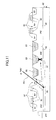
- Fig. 15 is a drawing illustrating the configuration of an apparatus for performing the method of placing circuit element cells.
- the apparatus for performing the method of placing circuit element cells is implemented as a computer such as a personal computer, an engineering workstation, or the like
- the apparatus of Fig. 15 includes a computer 510, a display apparatus 520 connected to the computer 510, a communication apparatus 523, and an input apparatus.
- the input apparatus includes a keyboard 521 and a mouse 522.
- the computer 510 includes a CPU 511, a ROM 513, a secondary storage device 514 such as a hard disk, a removable-medium storage device 515, and an interface 516.
- the keyboard 521 and mouse 522 provide user interface, and receive various commands for operating the computer 510 and user responses responding to data requests or the like.
- the display apparatus 520 displays the results of processing by the computer 510, and further displays various data that makes it possible for the user to communicate with the computer 510.
- the communication apparatus 523 provides for communication to be conducted with a remote site, and may include a modem, a network interface, or the like.
- the method of placing circuit element cells is provided as a computer program executable by the computer 510 and circuit element cell data usable by the computer program.
- This computer program and circuit element cell data are stored in a memory medium M that is mountable to the removable-medium storage device 515.
- the computer program and circuit element cell data are loaded to the RAM 512 or to the secondary storage device 514 from the memory medium M through the removable-medium storage device 515.
- the computer program and the circuit element cell data may be stored in a remote memory medium (not shown), and may be loaded to the RAM 512 or to the secondary storage device 514 from the remote memory medium through the communication apparatus 523 and the interface 516.
- the CPU 511 Upon user instruction for program execution entered through the keyboard 521 and/or the mouse 522, the CPU 511 loads the program to the RAM 512 from the memory medium M, the remote memory medium, or the secondary storage device 514. The CPU 511 executes the program loaded to the RAM 512 by use of an available memory space of the RAM 512 as a work area, and continues processing while communicating with the user as such a need arises.
- the ROM 513 stores therein control programs for the purpose of controlling basic operations of the computer 510.
- the user uses the computer 510 to place circuit element cells by use of the circuit element cell data including standard cells.
- the computer 510 displays a standard-cell placement area including a plurality of cell-placement rows on the display apparatus 520, and also displays a message that requests the user to specify the types and positions of circuit element cells.
- the CPU 511 executing the program may display a message requesting the placement of slit-shape well cells according to need.
- the circuit element cell 103 illustrated in Fig. 14 is placed, for example, such a message that requests the placement of slit-shape well cells is not displayed upon this cell placement action.
Landscapes
- Design And Manufacture Of Integrated Circuits (AREA)
- Semiconductor Integrated Circuits (AREA)
- Semiconductor Memories (AREA)
- Engineering & Computer Science (AREA)
- General Engineering & Computer Science (AREA)
Priority Applications (1)
| Application Number | Priority Date | Filing Date | Title |
|---|---|---|---|
| EP16173487.6A EP3104413B1 (de) | 2011-06-10 | 2012-05-14 | Integrierte halbleiterschaltung mit speicherzellen |
Applications Claiming Priority (1)
| Application Number | Priority Date | Filing Date | Title |
|---|---|---|---|
| JP2011130683A JP5741234B2 (ja) | 2011-06-10 | 2011-06-10 | セルの配置構造、半導体集積回路、及び回路素子セルの配置方法 |
Related Child Applications (2)
| Application Number | Title | Priority Date | Filing Date |
|---|---|---|---|
| EP16173487.6A Division-Into EP3104413B1 (de) | 2011-06-10 | 2012-05-14 | Integrierte halbleiterschaltung mit speicherzellen |
| EP16173487.6A Division EP3104413B1 (de) | 2011-06-10 | 2012-05-14 | Integrierte halbleiterschaltung mit speicherzellen |
Publications (3)
| Publication Number | Publication Date |
|---|---|
| EP2533286A2 true EP2533286A2 (de) | 2012-12-12 |
| EP2533286A3 EP2533286A3 (de) | 2016-09-28 |
| EP2533286B1 EP2533286B1 (de) | 2023-09-06 |
Family
ID=46062142
Family Applications (2)
| Application Number | Title | Priority Date | Filing Date |
|---|---|---|---|
| EP16173487.6A Active EP3104413B1 (de) | 2011-06-10 | 2012-05-14 | Integrierte halbleiterschaltung mit speicherzellen |
| EP12167829.6A Active EP2533286B1 (de) | 2011-06-10 | 2012-05-14 | Integrierte Halbleiterschaltung |
Family Applications Before (1)
| Application Number | Title | Priority Date | Filing Date |
|---|---|---|---|
| EP16173487.6A Active EP3104413B1 (de) | 2011-06-10 | 2012-05-14 | Integrierte halbleiterschaltung mit speicherzellen |
Country Status (3)
| Country | Link |
|---|---|
| US (1) | US9059036B2 (de) |
| EP (2) | EP3104413B1 (de) |
| JP (1) | JP5741234B2 (de) |
Families Citing this family (5)
| Publication number | Priority date | Publication date | Assignee | Title |
|---|---|---|---|---|
| US8645893B1 (en) * | 2012-10-23 | 2014-02-04 | Arm Limited | Method of generating a layout of an integrated circuit comprising both standard cells and at least one memory instance |
| CN105609504B (zh) * | 2015-12-25 | 2018-11-06 | 北京时代民芯科技有限公司 | 一种阱隔离型抗seu多节点翻转存储单元版图结构 |
| EP3229270A1 (de) * | 2016-04-06 | 2017-10-11 | IMEC vzw | Leistungsverteilungsnetzwerk für integrierte schaltungen |
| US10109619B2 (en) * | 2016-06-06 | 2018-10-23 | Qualcomm Incorporated | Methods and apparatus for using split N-well cells in a merged N-well block |
| KR102403735B1 (ko) | 2017-09-07 | 2022-05-30 | 삼성전자주식회사 | 비대칭적인 엔딩 셀들을 포함하는 집적 회로 및 시스템 온 칩 |
Citations (2)
| Publication number | Priority date | Publication date | Assignee | Title |
|---|---|---|---|---|
| JP2002353413A (ja) | 2001-05-28 | 2002-12-06 | Mitsubishi Electric Corp | 半導体記憶装置 |
| JP2010004019A (ja) | 2008-05-22 | 2010-01-07 | Nec Electronics Corp | 半導体集積回路 |
Family Cites Families (5)
| Publication number | Priority date | Publication date | Assignee | Title |
|---|---|---|---|---|
| JPH08330434A (ja) * | 1994-12-09 | 1996-12-13 | Mitsubishi Electric Corp | 半導体集積回路装置およびその配置配線方法並びにレイアウト方法 |
| JP4783022B2 (ja) | 2005-01-17 | 2011-09-28 | 株式会社東芝 | 半導体集積回路装置 |
| US7698681B2 (en) * | 2007-08-14 | 2010-04-13 | International Business Machines Corporation | Method for radiation tolerance by logic book folding |
| US7725870B2 (en) * | 2007-08-14 | 2010-05-25 | International Business Machines Corporation | Method for radiation tolerance by implant well notching |
| US8495550B2 (en) * | 2009-01-15 | 2013-07-23 | Klas Olof Lilja | Soft error hard electronic circuit and layout |
-
2011
- 2011-06-10 JP JP2011130683A patent/JP5741234B2/ja active Active
-
2012
- 2012-05-11 US US13/469,158 patent/US9059036B2/en active Active
- 2012-05-14 EP EP16173487.6A patent/EP3104413B1/de active Active
- 2012-05-14 EP EP12167829.6A patent/EP2533286B1/de active Active
Patent Citations (2)
| Publication number | Priority date | Publication date | Assignee | Title |
|---|---|---|---|---|
| JP2002353413A (ja) | 2001-05-28 | 2002-12-06 | Mitsubishi Electric Corp | 半導体記憶装置 |
| JP2010004019A (ja) | 2008-05-22 | 2010-01-07 | Nec Electronics Corp | 半導体集積回路 |
Also Published As
| Publication number | Publication date |
|---|---|
| EP2533286A3 (de) | 2016-09-28 |
| US9059036B2 (en) | 2015-06-16 |
| EP3104413A1 (de) | 2016-12-14 |
| JP2013004542A (ja) | 2013-01-07 |
| EP3104413B1 (de) | 2023-09-06 |
| US20120313185A1 (en) | 2012-12-13 |
| JP5741234B2 (ja) | 2015-07-01 |
| EP2533286B1 (de) | 2023-09-06 |
Similar Documents
| Publication | Publication Date | Title |
|---|---|---|
| US11195797B2 (en) | Applications of buried power rails | |
| CN111066153B (zh) | 鳍式场效晶体管技术中的半导体布局 | |
| US9059036B2 (en) | Semiconductor integrated circuit including memory cells | |
| US9786645B2 (en) | Integrated circuit | |
| US7750373B2 (en) | Semiconductor integrated circuit | |
| US7923756B2 (en) | Metal oxide semiconductor (MOS) device comprising a buried region under drain | |
| US20050040435A1 (en) | Semiconductor integrated circuit device and its manufacture using automatic layout | |
| US20140217513A1 (en) | Semiconductor integrated circuit device | |
| US20170243888A1 (en) | Layout structure for semiconductor integrated circuit | |
| EP2698820A2 (de) | Schaltungslayoutoptimierung für Technologien weit unterhalb des Mikrometerbereichs | |
| US9430602B2 (en) | Semiconductor integrated circuit device and method for designing layout of the same having standard cells, basic cells and a protective diode cell | |
| US8884349B2 (en) | Semiconductor device | |
| CN110637358A (zh) | 半导体集成电路装置 | |
| JP4783022B2 (ja) | 半導体集積回路装置 | |
| US8445943B2 (en) | Semiconductor integrated circuit device | |
| JP2021153078A (ja) | 半導体装置 | |
| US9941284B2 (en) | Semiconductor device | |
| US20230178537A1 (en) | Semiconductor structure of hybrid cell array | |
| US20220399248A1 (en) | Integrated cooling device based on peltier effect and manufacturing method thereof | |
| JPWO2020144767A1 (ja) | 半導体集積回路装置 | |
| CN103811487A (zh) | 抑制单粒子效应电荷扩散的数字集成电路填充单元 | |
| JP4761914B2 (ja) | スタンダードセルライブラリ、半導体集積回路の設計方法、半導体集積回路パターンおよび半導体集積回路 | |
| JP2011054772A (ja) | 半導体装置 | |
| JP2008004699A (ja) | 半導体記憶装置 | |
| US20060208317A1 (en) | Layout structure of semiconductor cells |
Legal Events
| Date | Code | Title | Description |
|---|---|---|---|
| PUAI | Public reference made under article 153(3) epc to a published international application that has entered the european phase |
Free format text: ORIGINAL CODE: 0009012 |
|
| AK | Designated contracting states |
Kind code of ref document: A2 Designated state(s): AL AT BE BG CH CY CZ DE DK EE ES FI FR GB GR HR HU IE IS IT LI LT LU LV MC MK MT NL NO PL PT RO RS SE SI SK SM TR |
|
| AX | Request for extension of the european patent |
Extension state: BA ME |
|
| PUAL | Search report despatched |
Free format text: ORIGINAL CODE: 0009013 |
|
| AK | Designated contracting states |
Kind code of ref document: A3 Designated state(s): AL AT BE BG CH CY CZ DE DK EE ES FI FR GB GR HR HU IE IS IT LI LT LU LV MC MK MT NL NO PL PT RO RS SE SI SK SM TR |
|
| AX | Request for extension of the european patent |
Extension state: BA ME |
|
| RIC1 | Information provided on ipc code assigned before grant |
Ipc: H01L 27/02 20060101AFI20160825BHEP Ipc: H01L 27/118 20060101ALI20160825BHEP |
|
| STAA | Information on the status of an ep patent application or granted ep patent |
Free format text: STATUS: REQUEST FOR EXAMINATION WAS MADE |
|
| 17P | Request for examination filed |
Effective date: 20170313 |
|
| RBV | Designated contracting states (corrected) |
Designated state(s): AL AT BE BG CH CY CZ DE DK EE ES FI FR GB GR HR HU IE IS IT LI LT LU LV MC MK MT NL NO PL PT RO RS SE SI SK SM TR |
|
| STAA | Information on the status of an ep patent application or granted ep patent |
Free format text: STATUS: EXAMINATION IS IN PROGRESS |
|
| 17Q | First examination report despatched |
Effective date: 20191016 |
|
| GRAP | Despatch of communication of intention to grant a patent |
Free format text: ORIGINAL CODE: EPIDOSNIGR1 |
|
| STAA | Information on the status of an ep patent application or granted ep patent |
Free format text: STATUS: GRANT OF PATENT IS INTENDED |
|
| INTG | Intention to grant announced |
Effective date: 20230330 |
|
| GRAS | Grant fee paid |
Free format text: ORIGINAL CODE: EPIDOSNIGR3 |
|
| GRAA | (expected) grant |
Free format text: ORIGINAL CODE: 0009210 |
|
| STAA | Information on the status of an ep patent application or granted ep patent |
Free format text: STATUS: THE PATENT HAS BEEN GRANTED |
|
| AK | Designated contracting states |
Kind code of ref document: B1 Designated state(s): AL AT BE BG CH CY CZ DE DK EE ES FI FR GB GR HR HU IE IS IT LI LT LU LV MC MK MT NL NO PL PT RO RS SE SI SK SM TR |
|
| REG | Reference to a national code |
Ref country code: GB Ref legal event code: FG4D |
|
| REG | Reference to a national code |
Ref country code: CH Ref legal event code: EP |
|
| REG | Reference to a national code |
Ref country code: IE Ref legal event code: FG4D |
|
| REG | Reference to a national code |
Ref country code: DE Ref legal event code: R096 Ref document number: 602012080042 Country of ref document: DE |
|
| REG | Reference to a national code |
Ref country code: LT Ref legal event code: MG9D |
|
| REG | Reference to a national code |
Ref country code: NL Ref legal event code: MP Effective date: 20230906 |
|
| PG25 | Lapsed in a contracting state [announced via postgrant information from national office to epo] |
Ref country code: GR Free format text: LAPSE BECAUSE OF FAILURE TO SUBMIT A TRANSLATION OF THE DESCRIPTION OR TO PAY THE FEE WITHIN THE PRESCRIBED TIME-LIMIT Effective date: 20231207 |
|
| PG25 | Lapsed in a contracting state [announced via postgrant information from national office to epo] |
Ref country code: SE Free format text: LAPSE BECAUSE OF FAILURE TO SUBMIT A TRANSLATION OF THE DESCRIPTION OR TO PAY THE FEE WITHIN THE PRESCRIBED TIME-LIMIT Effective date: 20230906 Ref country code: RS Free format text: LAPSE BECAUSE OF FAILURE TO SUBMIT A TRANSLATION OF THE DESCRIPTION OR TO PAY THE FEE WITHIN THE PRESCRIBED TIME-LIMIT Effective date: 20230906 Ref country code: NO Free format text: LAPSE BECAUSE OF FAILURE TO SUBMIT A TRANSLATION OF THE DESCRIPTION OR TO PAY THE FEE WITHIN THE PRESCRIBED TIME-LIMIT Effective date: 20231206 Ref country code: LV Free format text: LAPSE BECAUSE OF FAILURE TO SUBMIT A TRANSLATION OF THE DESCRIPTION OR TO PAY THE FEE WITHIN THE PRESCRIBED TIME-LIMIT Effective date: 20230906 Ref country code: LT Free format text: LAPSE BECAUSE OF FAILURE TO SUBMIT A TRANSLATION OF THE DESCRIPTION OR TO PAY THE FEE WITHIN THE PRESCRIBED TIME-LIMIT Effective date: 20230906 Ref country code: HR Free format text: LAPSE BECAUSE OF FAILURE TO SUBMIT A TRANSLATION OF THE DESCRIPTION OR TO PAY THE FEE WITHIN THE PRESCRIBED TIME-LIMIT Effective date: 20230906 Ref country code: GR Free format text: LAPSE BECAUSE OF FAILURE TO SUBMIT A TRANSLATION OF THE DESCRIPTION OR TO PAY THE FEE WITHIN THE PRESCRIBED TIME-LIMIT Effective date: 20231207 Ref country code: FI Free format text: LAPSE BECAUSE OF FAILURE TO SUBMIT A TRANSLATION OF THE DESCRIPTION OR TO PAY THE FEE WITHIN THE PRESCRIBED TIME-LIMIT Effective date: 20230906 |
|
| REG | Reference to a national code |
Ref country code: AT Ref legal event code: MK05 Ref document number: 1609701 Country of ref document: AT Kind code of ref document: T Effective date: 20230906 |
|
| PG25 | Lapsed in a contracting state [announced via postgrant information from national office to epo] |
Ref country code: NL Free format text: LAPSE BECAUSE OF FAILURE TO SUBMIT A TRANSLATION OF THE DESCRIPTION OR TO PAY THE FEE WITHIN THE PRESCRIBED TIME-LIMIT Effective date: 20230906 |
|
| PG25 | Lapsed in a contracting state [announced via postgrant information from national office to epo] |
Ref country code: IS Free format text: LAPSE BECAUSE OF FAILURE TO SUBMIT A TRANSLATION OF THE DESCRIPTION OR TO PAY THE FEE WITHIN THE PRESCRIBED TIME-LIMIT Effective date: 20240106 |
|
| PG25 | Lapsed in a contracting state [announced via postgrant information from national office to epo] |
Ref country code: AT Free format text: LAPSE BECAUSE OF FAILURE TO SUBMIT A TRANSLATION OF THE DESCRIPTION OR TO PAY THE FEE WITHIN THE PRESCRIBED TIME-LIMIT Effective date: 20230906 |
|
| PG25 | Lapsed in a contracting state [announced via postgrant information from national office to epo] |
Ref country code: ES Free format text: LAPSE BECAUSE OF FAILURE TO SUBMIT A TRANSLATION OF THE DESCRIPTION OR TO PAY THE FEE WITHIN THE PRESCRIBED TIME-LIMIT Effective date: 20230906 |
|
| PG25 | Lapsed in a contracting state [announced via postgrant information from national office to epo] |
Ref country code: SM Free format text: LAPSE BECAUSE OF FAILURE TO SUBMIT A TRANSLATION OF THE DESCRIPTION OR TO PAY THE FEE WITHIN THE PRESCRIBED TIME-LIMIT Effective date: 20230906 Ref country code: RO Free format text: LAPSE BECAUSE OF FAILURE TO SUBMIT A TRANSLATION OF THE DESCRIPTION OR TO PAY THE FEE WITHIN THE PRESCRIBED TIME-LIMIT Effective date: 20230906 Ref country code: IS Free format text: LAPSE BECAUSE OF FAILURE TO SUBMIT A TRANSLATION OF THE DESCRIPTION OR TO PAY THE FEE WITHIN THE PRESCRIBED TIME-LIMIT Effective date: 20240106 Ref country code: ES Free format text: LAPSE BECAUSE OF FAILURE TO SUBMIT A TRANSLATION OF THE DESCRIPTION OR TO PAY THE FEE WITHIN THE PRESCRIBED TIME-LIMIT Effective date: 20230906 Ref country code: EE Free format text: LAPSE BECAUSE OF FAILURE TO SUBMIT A TRANSLATION OF THE DESCRIPTION OR TO PAY THE FEE WITHIN THE PRESCRIBED TIME-LIMIT Effective date: 20230906 Ref country code: CZ Free format text: LAPSE BECAUSE OF FAILURE TO SUBMIT A TRANSLATION OF THE DESCRIPTION OR TO PAY THE FEE WITHIN THE PRESCRIBED TIME-LIMIT Effective date: 20230906 Ref country code: AT Free format text: LAPSE BECAUSE OF FAILURE TO SUBMIT A TRANSLATION OF THE DESCRIPTION OR TO PAY THE FEE WITHIN THE PRESCRIBED TIME-LIMIT Effective date: 20230906 Ref country code: SK Free format text: LAPSE BECAUSE OF FAILURE TO SUBMIT A TRANSLATION OF THE DESCRIPTION OR TO PAY THE FEE WITHIN THE PRESCRIBED TIME-LIMIT Effective date: 20230906 Ref country code: PT Free format text: LAPSE BECAUSE OF FAILURE TO SUBMIT A TRANSLATION OF THE DESCRIPTION OR TO PAY THE FEE WITHIN THE PRESCRIBED TIME-LIMIT Effective date: 20240108 |
|
| PG25 | Lapsed in a contracting state [announced via postgrant information from national office to epo] |
Ref country code: PL Free format text: LAPSE BECAUSE OF FAILURE TO SUBMIT A TRANSLATION OF THE DESCRIPTION OR TO PAY THE FEE WITHIN THE PRESCRIBED TIME-LIMIT Effective date: 20230906 Ref country code: IT Free format text: LAPSE BECAUSE OF FAILURE TO SUBMIT A TRANSLATION OF THE DESCRIPTION OR TO PAY THE FEE WITHIN THE PRESCRIBED TIME-LIMIT Effective date: 20230906 |
|
| REG | Reference to a national code |
Ref country code: DE Ref legal event code: R097 Ref document number: 602012080042 Country of ref document: DE |
|
| PG25 | Lapsed in a contracting state [announced via postgrant information from national office to epo] |
Ref country code: DK Free format text: LAPSE BECAUSE OF FAILURE TO SUBMIT A TRANSLATION OF THE DESCRIPTION OR TO PAY THE FEE WITHIN THE PRESCRIBED TIME-LIMIT Effective date: 20230906 |
|
| PLBE | No opposition filed within time limit |
Free format text: ORIGINAL CODE: 0009261 |
|
| STAA | Information on the status of an ep patent application or granted ep patent |
Free format text: STATUS: NO OPPOSITION FILED WITHIN TIME LIMIT |
|
| PG25 | Lapsed in a contracting state [announced via postgrant information from national office to epo] |
Ref country code: DK Free format text: LAPSE BECAUSE OF FAILURE TO SUBMIT A TRANSLATION OF THE DESCRIPTION OR TO PAY THE FEE WITHIN THE PRESCRIBED TIME-LIMIT Effective date: 20230906 Ref country code: SI Free format text: LAPSE BECAUSE OF FAILURE TO SUBMIT A TRANSLATION OF THE DESCRIPTION OR TO PAY THE FEE WITHIN THE PRESCRIBED TIME-LIMIT Effective date: 20230906 |
|
| 26N | No opposition filed |
Effective date: 20240607 |
|
| PG25 | Lapsed in a contracting state [announced via postgrant information from national office to epo] |
Ref country code: BG Free format text: LAPSE BECAUSE OF FAILURE TO SUBMIT A TRANSLATION OF THE DESCRIPTION OR TO PAY THE FEE WITHIN THE PRESCRIBED TIME-LIMIT Effective date: 20230906 |
|
| REG | Reference to a national code |
Ref country code: DE Ref legal event code: R079 Ref document number: 602012080042 Country of ref document: DE Free format text: PREVIOUS MAIN CLASS: H01L0027020000 Ipc: H10D0089000000 |
|
| PG25 | Lapsed in a contracting state [announced via postgrant information from national office to epo] |
Ref country code: BG Free format text: LAPSE BECAUSE OF FAILURE TO SUBMIT A TRANSLATION OF THE DESCRIPTION OR TO PAY THE FEE WITHIN THE PRESCRIBED TIME-LIMIT Effective date: 20230906 |
|
| REG | Reference to a national code |
Ref country code: CH Ref legal event code: PL |
|
| PG25 | Lapsed in a contracting state [announced via postgrant information from national office to epo] |
Ref country code: MC Free format text: LAPSE BECAUSE OF FAILURE TO SUBMIT A TRANSLATION OF THE DESCRIPTION OR TO PAY THE FEE WITHIN THE PRESCRIBED TIME-LIMIT Effective date: 20230906 |
|
| PG25 | Lapsed in a contracting state [announced via postgrant information from national office to epo] |
Ref country code: LU Free format text: LAPSE BECAUSE OF NON-PAYMENT OF DUE FEES Effective date: 20240514 |
|
| PG25 | Lapsed in a contracting state [announced via postgrant information from national office to epo] |
Ref country code: MC Free format text: LAPSE BECAUSE OF FAILURE TO SUBMIT A TRANSLATION OF THE DESCRIPTION OR TO PAY THE FEE WITHIN THE PRESCRIBED TIME-LIMIT Effective date: 20230906 Ref country code: LU Free format text: LAPSE BECAUSE OF NON-PAYMENT OF DUE FEES Effective date: 20240514 Ref country code: CH Free format text: LAPSE BECAUSE OF NON-PAYMENT OF DUE FEES Effective date: 20240531 |
|
| REG | Reference to a national code |
Ref country code: BE Ref legal event code: MM Effective date: 20240531 |
|
| PG25 | Lapsed in a contracting state [announced via postgrant information from national office to epo] |
Ref country code: IE Free format text: LAPSE BECAUSE OF NON-PAYMENT OF DUE FEES Effective date: 20240514 |
|
| PG25 | Lapsed in a contracting state [announced via postgrant information from national office to epo] |
Ref country code: BE Free format text: LAPSE BECAUSE OF NON-PAYMENT OF DUE FEES Effective date: 20240531 |
|
| PGFP | Annual fee paid to national office [announced via postgrant information from national office to epo] |
Ref country code: DE Payment date: 20250423 Year of fee payment: 14 |
|
| PGFP | Annual fee paid to national office [announced via postgrant information from national office to epo] |
Ref country code: GB Payment date: 20250423 Year of fee payment: 14 |
|
| PGFP | Annual fee paid to national office [announced via postgrant information from national office to epo] |
Ref country code: FR Payment date: 20250424 Year of fee payment: 14 |
|
| PG25 | Lapsed in a contracting state [announced via postgrant information from national office to epo] |
Ref country code: CY Free format text: LAPSE BECAUSE OF FAILURE TO SUBMIT A TRANSLATION OF THE DESCRIPTION OR TO PAY THE FEE WITHIN THE PRESCRIBED TIME-LIMIT; INVALID AB INITIO Effective date: 20120514 |
|
| PG25 | Lapsed in a contracting state [announced via postgrant information from national office to epo] |
Ref country code: HU Free format text: LAPSE BECAUSE OF FAILURE TO SUBMIT A TRANSLATION OF THE DESCRIPTION OR TO PAY THE FEE WITHIN THE PRESCRIBED TIME-LIMIT; INVALID AB INITIO Effective date: 20120514 |