EP2533292A2 - Transistor à haute mobilité d'électrons (HEMT) de groupe III-V à enrichissement et procédé de fabrication - Google Patents
Transistor à haute mobilité d'électrons (HEMT) de groupe III-V à enrichissement et procédé de fabrication Download PDFInfo
- Publication number
- EP2533292A2 EP2533292A2 EP12168132A EP12168132A EP2533292A2 EP 2533292 A2 EP2533292 A2 EP 2533292A2 EP 12168132 A EP12168132 A EP 12168132A EP 12168132 A EP12168132 A EP 12168132A EP 2533292 A2 EP2533292 A2 EP 2533292A2
- Authority
- EP
- European Patent Office
- Prior art keywords
- group iii
- gate
- enhancement mode
- hemt
- barrier layer
- Prior art date
- Legal status (The legal status is an assumption and is not a legal conclusion. Google has not performed a legal analysis and makes no representation as to the accuracy of the status listed.)
- Withdrawn
Links
Images


Classifications
-
- H—ELECTRICITY
- H10—SEMICONDUCTOR DEVICES; ELECTRIC SOLID-STATE DEVICES NOT OTHERWISE PROVIDED FOR
- H10D—INORGANIC ELECTRIC SEMICONDUCTOR DEVICES
- H10D30/00—Field-effect transistors [FET]
- H10D30/40—FETs having zero-dimensional [0D], one-dimensional [1D] or two-dimensional [2D] charge carrier gas channels
- H10D30/47—FETs having zero-dimensional [0D], one-dimensional [1D] or two-dimensional [2D] charge carrier gas channels having two-dimensional [2D] charge carrier gas channels, e.g. nanoribbon FETs or high electron mobility transistors [HEMT]
- H10D30/471—High electron mobility transistors [HEMT] or high hole mobility transistors [HHMT]
- H10D30/475—High electron mobility transistors [HEMT] or high hole mobility transistors [HHMT] having wider bandgap layer formed on top of lower bandgap active layer, e.g. undoped barrier HEMTs such as i-AlGaN/GaN HEMTs
-
- H—ELECTRICITY
- H10—SEMICONDUCTOR DEVICES; ELECTRIC SOLID-STATE DEVICES NOT OTHERWISE PROVIDED FOR
- H10D—INORGANIC ELECTRIC SEMICONDUCTOR DEVICES
- H10D30/00—Field-effect transistors [FET]
- H10D30/01—Manufacture or treatment
- H10D30/015—Manufacture or treatment of FETs having heterojunction interface channels or heterojunction gate electrodes, e.g. HEMT
-
- H—ELECTRICITY
- H10—SEMICONDUCTOR DEVICES; ELECTRIC SOLID-STATE DEVICES NOT OTHERWISE PROVIDED FOR
- H10D—INORGANIC ELECTRIC SEMICONDUCTOR DEVICES
- H10D62/00—Semiconductor bodies, or regions thereof, of devices having potential barriers
- H10D62/10—Shapes, relative sizes or dispositions of the regions of the semiconductor bodies; Shapes of the semiconductor bodies
- H10D62/17—Semiconductor regions connected to electrodes not carrying current to be rectified, amplified or switched, e.g. channel regions
- H10D62/343—Gate regions of field-effect devices having PN junction gates
-
- H—ELECTRICITY
- H10—SEMICONDUCTOR DEVICES; ELECTRIC SOLID-STATE DEVICES NOT OTHERWISE PROVIDED FOR
- H10D—INORGANIC ELECTRIC SEMICONDUCTOR DEVICES
- H10D62/00—Semiconductor bodies, or regions thereof, of devices having potential barriers
- H10D62/80—Semiconductor bodies, or regions thereof, of devices having potential barriers characterised by the materials
- H10D62/85—Semiconductor bodies, or regions thereof, of devices having potential barriers characterised by the materials being Group III-V materials, e.g. GaAs
- H10D62/8503—Nitride Group III-V materials, e.g. AlN or GaN
Definitions
- group III-V semiconductor refers to a compound semiconductor that includes at least one group III element and at least one group V element, such as, but not limited to, gallium nitride (GaN), aluminum gallium nitride (AlGaN), gallium arsenide (GaAs), indium aluminum gallium nitride (InAlGaN), indium gallium nitride (InGaN) and the like.
- III-nitride semiconductor refers to a compound semiconductor that includes nitrogen and at least one group III element, such as, but not limited to, GaN, AlGaN, InN, AIN, InGaN, InAlGaN and the like.
- the present invention is generally in the field of semiconductors. More specifically, the present invention is in the field of group III-V high electron mobility transistor (HEMT) fabrication.
- HEMT high electron mobility transistor
- High electron mobility transistors utilizing group III-V heterojunction structures, such as III-nitride heterojunctions, typically operate using piezoelectric polarization fields to generate a two dimensional electron gas (2DEG) that allows for high current densities with low resistive losses.
- the 2DEG can arise naturally at an interface of the III-nitride materials forming the heterojunction and, due to the 2DEG, conventional III-nitride HEMTs typically conduct without the application of a gate potential. That is to say, conventional III-nitride and other group III-V HEMTs tend to be normally ON, or depletion mode devices.
- III-nitride HEMTs are advantageous when used in power applications, the normally ON nature of conventional III-nitride HEMT structures can introduce problems when such depletion mode transistors are used as power devices. For example, in power applications it is desirable to avoid conducting current through the III-nitride HEMTs before control circuitry is fully powered and operational. Accordingly, it would be desirable to provide III-nitride HEMTs that are normally OFF, or enhancement mode transistors to, for example, avoid current conduction problems during start-up and other circuit transitions.
- the present invention is directed to an enhancement mode group III-V high electron mobility transistor (HEMT) and method for fabrication, substantially as shown in and/or described in connection with at least one of the figures, as set forth more completely in the claims.
- HEMT high electron mobility transistor
- the present invention is directed to an enhancement mode group III-V high electron mobility transistor (HEMT) and method for fabrication.
- HEMT high electron mobility transistor
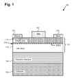
- FIG. 1 is a cross-sectional view of a structure corresponding to a conventional depletion mode group III-V HEMT, showing its normally ON state.
- structure 100 comprises a III-nitride HEMT implemented as a gallium nitride (GaN) device.
- Structure 100 includes support substrate 102, transition structure 104, heterojunction 116 comprising GaN body 112 and aluminum gallium nitride (AlGaN) barrier layer 114, source contact 172, drain contact 174, and gate 162.
- GaN gallium nitride
- 2DEG two dimensional electron gas
- 2DEG 118 provides a conduction channel for the charge carriers of the HEMT and is generated at the interface of GaN body 112 and AlGaN barrier layer 114, in heterojunction 116.
- 2DEG 118 produced by heterojunction 116 provides a continuous, uninterrupted channel for the flow of current between source contact 172 and drain contact 174.
- the conventional III-nitride HEMT comprised by conventional structure 100 is a normally ON, depletion mode, device.
- III-nitride HEMTs such as the GaN HEMT comprised of conventional structure 100 in Figure 1
- their normally ON nature can introduce problems in power applications.
- Figure 2 shows flowchart 200 presenting a method, according to one embodiment of the present invention, for fabricating an enhancement mode group III-V HEMT configured to overcome the drawbacks and deficiencies associated with conventional structure 100, in Figure 1 .
- Certain details and features have been left out of flowchart 200 that are apparent to a person of ordinary skill in the art.
- a step may comprise one or more substeps or may involve specialized equipment or materials, as known in the art.
- steps 210 through 260 indicated in flowchart 200 are sufficient to describe one embodiment of the present invention, other embodiments of the invention may utilize steps different from those shown in flowchart 200, and may include more, or fewer, steps.
- structure 310 of Figure 3A corresponds to a cross-sectional view of an enhancement mode group III-V HEMT at an initial fabrication stage, according to one embodiment of the present invention.
- Structure 310 shows substrate 302 suitable for use as a support substrate for an enhancement mode group III-V HEMT.
- Figure 3A shows structure 310 at a stage of fabrication following processing step 210 of flowchart 200.
- structures 320, 330, 340, 350, and 360 show the result of performing, on structure 310, steps 220, 230, 240, 250, and 260 of flowchart 200 of Figure 2 , respectively.
- structure 320 shows structure 310 following processing step 220
- structure 330 shows structure 310 following processing step 230, and so forth.
- the structures shown in Figures 3A through 3F are provided as specific implementations of the present inventive principles, and are shown with such specificity for the purposes of conceptual clarity. It should also be understood that particular details such as the materials used to form structures 310 through 360 and 400, and the techniques used to produce the various depicted features, are being provided as examples, and should not be interpreted as limitations.
- step 210 of flowchart 200 comprises providing substrate 302 for fabrication of an enhancement mode group III-V HEMT.
- Substrate 302 may comprise any material suitable for use as a substrate for fabrication of a group III-V semiconductor device.
- substrate 302 may comprise silicon (Si), silicon carbide (SiC), or sapphire.
- substrate 302 may comprise a native substrate for the materials from which the group III-V semiconductor device is to be fabricated, and may be a native GaN or other III-nitride substrate, for instance.
- substrate 302 is shown as a substantially unitary substrate, in other embodiments, substrate 302 may correspond to a semiconductor on insulator substrate such, as a silicon on insulator (SOI) or germanium on insulator (GOI) substrate, for example.
- SOI silicon on insulator
- GOI germanium on insulator
- step 220 of flowchart 200 comprises forming GaN body 312 over substrate 302.
- transition structure 304 may be formed between substrate 302 and GaN body 312.
- substrate 302 is a silicon substrate
- transition structure 304 may correspond to a plurality of distinguishable layers mediating the lattice transition from substrate 302 to GaN body 312, thereby reducing lattice mismatch between substrate 302 and GaN body 312.
- transition structure 304 may include an aluminum nitride (AIN) layer formed on substrate 302, and a series of AlGaN layers comprising progressively less aluminum and more gallium, until a suitable transition to GaN body 312 is achieved.
- AIN aluminum nitride
- GaN body 312 may be formed over substrate 302 using any of a number of conventional growth techniques.
- GaN body 312 may be formed over transition structure 304 using molecular-beam epitaxy (MBE), metalorganic chemical vapor deposition (MOCVD), or hydride vapor phase epitaxy (HVPE), to name a few suitable approaches.
- MBE molecular-beam epitaxy
- MOCVD metalorganic chemical vapor deposition
- HVPE hydride vapor phase epitaxy
- step 230 of flowchart 200 comprises forming AlGaN barrier layer 314 over GaN body 312, thereby forming heterojunction 316 giving rise to 2DEG 318.
- AlGaN barrier layer 314 may be formed over GaN body 312 using any of MBE, MOCVD, or HVPE, for example.
- Heterojunction 316 including GaN body 312 and AlGaN barrier layer 314 may be undoped, in which case defects typically produced during growth of GaN body 312 and AlGaN barrier layer 314 result in heterojunction 316 being characterized by a light N type conductivity.
- heterojunction 316 may intentionally include an N type conductivity GaN body 312 and/or an N type conductivity AlGaN barrier layer 314.
- Figure 3C is not necessarily drawn to scale.
- GaN body 312 and AlGaN barrier layer 314 are shown as having comparable thicknesses as a visual aid, those features will typically have distinctly different respective thicknesses, such as a thicknesses up to approximately 10 ⁇ m for GaN body 312 and a thickness of less than approximately 50 nm for AlGaN barrier layer 314, for example.
- heterojunction 316 typically the only constraints placed upon the constituents of heterojunction 316 are that barrier layer 314 comprise a group III-V semiconductor having a wider band gap than the group III-V semiconductor forming body 312, and that both group III-V semiconductors be selected so as to produce 2DEG 318 at their heterojunction interface.
- barrier layer 314 comprise a group III-V semiconductor having a wider band gap than the group III-V semiconductor forming body 312, and that both group III-V semiconductors be selected so as to produce 2DEG 318 at their heterojunction interface.
- Such a heterojunction may be formed using GaN, as represented in the present figures, or any other suitable group III-V semiconductor materials, as described in the "Definition" section above.
- step 240 of flowchart 200 comprises forming hard mask 342 over AlGaN barrier layer 314 and creating opening 344 in hard mask 342 so as to expose a portion of AlGaN barrier layer 314.
- Hard mask 342 may comprise silicon dioxide (SiO 2 ) or silicon nitride (Si 3 N 4 ), for example, and may be deposited over AlGaN barrier layer 314 using a plasma enhanced chemical vapor deposition (PECVD) process.
- PECVD plasma enhanced chemical vapor deposition
- Hard mask 342 may be further processed to define opening 344, through an etch process, for example.
- masking of AlGaN barrier layer 314, in step 240 of flowchart 200 is characterized as being performed using hard mask 342 in the present embodiment, more generally, masking may be performed using either a hard mask, as represented in Figure 2 , or using a soft mask material, such as photoresist or another type of polymer mask, for example.
- step 250 of flowchart 200 comprises selectively forming P type III-nitride gate layer 352 over AlGaN barrier layer 314, in opening 344.
- P type III-nitride gate layer 352 may comprise P type AlGaN or P type GaN, for example.
- a P type gate layer corresponding to P type III-nitride gate layer 352 may comprise any suitable P type group III-V semiconductor material.
- P type III-nitride gate layer 352 may be selectively formed in opening 344 using an MOCVD process, for example. As shown in Figure 3E , the presence of P type III-nitride gate layer 352 over AlGaN barrier layer 314 interrupts 2DEG 318 under P type III-nitride gate layer 352. As may be understood by one of ordinary skill in the art, disposition of P type III-nitride gate layer 352 over at least nominally N type AlGaN barrier layer 314 produces a PN junction that substantially depletes 2DEG 318 under P type III-nitride gate layer 352, thereby preventing formation of 2DEG 318 under the P type gate layer 352.
- steps 210-230 may be followed by formation of a P type III-nitride material layer, for example as a blanket layer over AlGaN barrier layer 314.
- Such a layer of P type III-nitride material could then be suitably masked to protect a region of the P type III-nitride material layer corresponding to P type III-nitride gate layer 352, and the unprotected portions of the P type III-nitride material layer could be removed, leaving P type III-nitride gate layer 352.
- step 260 of flowchart 200 comprises completing fabrication of gate structure 362, which includes P type III-nitride gate layer 352.
- gate structure 362 comprises conductive gate electrode 364 formed over P type III-nitride gate layer 352.
- Conductive gate electrode 364 may comprise any suitable conductive material, such as doped polysilicon, for example, or a metal such as titanium (Ti) or aluminum (Al).
- gate structure 362 may further comprise gate dielectric 366 formed over P type III-nitride gate layer 352.
- Gate dielectric 366 may be disposed between P type III-nitride gate layer 352 and conductive gate electrode 364, and may comprise aluminum oxide (Al 2 O 3 ), silicon dioxide (SiO 2 ) or silicon nitride (Si 3 N 4 ), for example.
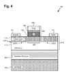
- Figure 4 shows a cross-sectional view of structure 400 corresponding to an enhancement mode group III-V HEMT, according to one embodiment of the present invention.
- Structure 400 may be fabricated according to the method of flowchart 200, in Figure 2 , for example, wherein the method of flowchart 200 further comprises forming respective ohmic source and drain contacts 472 and 474.
- structure 400 includes gate structure 462 formed over heterojunction 416 and preventing formation of 2DEG 418 under gate structure 462.
- Gate structure 462 including P type III-nitride gate layer 452, conductive gate electrode 464, and gate dielectric 466 corresponds to gate structure 362 including P type III-nitride gate layer 352, conductive gate electrode 364, and gate dielectric 366, in Figure 3F
- heterojunction 416 including GaN body 412, AlGaN barrier layer 414, and interrupted 2DEG 418 in Figure 4
- heterojunction 316 including GaN body 312, AlGaN barrier layer 314, and interrupted 2DEG 318 in Figures 3E and 3F
- substrate 402 and transition structure 404, in Figure 4 correspond respectively to substrate 302, shown in Figures 3A through 3F
- transition structure 304 shown in Figures 3B through 3F .
- III-nitride HEMT As illustrated in Figure 4 , and for the reasons previously described, in the absence of an applied gate voltage, inclusion of P type III-nitride gate layer 452 as part of gate structure 462 prevents 2DEG 418 from being formed under gate structure 462, resulting in 2DEG interruption 468. Consequently, the III-nitride HEMT shown in Figure 4 is a normally OFF, or enhancement mode device. Affirmative application of a suitable gate voltage to conductive gate electrode 464 of gate structure 462 results in removal of 2DEG interruption 468 and establishment of a continuous high electron mobility 2DEG channel coupling source contact 472 and drain contact 474 through heterojunction 416 on an on-demand basis.
Landscapes
- Junction Field-Effect Transistors (AREA)
- Insulated Gate Type Field-Effect Transistor (AREA)
Applications Claiming Priority (1)
| Application Number | Priority Date | Filing Date | Title |
|---|---|---|---|
| US13/157,562 US8604486B2 (en) | 2011-06-10 | 2011-06-10 | Enhancement mode group III-V high electron mobility transistor (HEMT) and method for fabrication |
Publications (2)
| Publication Number | Publication Date |
|---|---|
| EP2533292A2 true EP2533292A2 (fr) | 2012-12-12 |
| EP2533292A3 EP2533292A3 (fr) | 2017-05-03 |
Family
ID=46172672
Family Applications (1)
| Application Number | Title | Priority Date | Filing Date |
|---|---|---|---|
| EP12168132.4A Withdrawn EP2533292A3 (fr) | 2011-06-10 | 2012-05-15 | Transistor à haute mobilité d'électrons (HEMT) de groupe III-V à enrichissement et procédé de fabrication |
Country Status (3)
| Country | Link |
|---|---|
| US (1) | US8604486B2 (fr) |
| EP (1) | EP2533292A3 (fr) |
| JP (1) | JP2013004967A (fr) |
Cited By (2)
| Publication number | Priority date | Publication date | Assignee | Title |
|---|---|---|---|---|
| CN109860289A (zh) * | 2018-12-04 | 2019-06-07 | 北京大学深圳研究生院 | 一种晶体管及其制作方法 |
| TWI764475B (zh) * | 2020-12-28 | 2022-05-11 | 國家中山科學研究院 | P型摻雜層電極偏移之增強型氮化鎵元件 |
Families Citing this family (38)
| Publication number | Priority date | Publication date | Assignee | Title |
|---|---|---|---|---|
| JP2013048212A (ja) * | 2011-07-28 | 2013-03-07 | Sony Corp | 半導体装置および半導体装置の製造方法 |
| JP6054620B2 (ja) * | 2012-03-29 | 2016-12-27 | トランスフォーム・ジャパン株式会社 | 化合物半導体装置及びその製造方法 |
| JP5985337B2 (ja) * | 2012-09-28 | 2016-09-06 | ルネサスエレクトロニクス株式会社 | 半導体装置およびその製造方法 |
| US8895992B2 (en) | 2013-02-22 | 2014-11-25 | Taiwan Semiconductor Manufacturing Company, Ltd. | High electron mobility transistor and method of forming the same |
| US8928037B2 (en) * | 2013-02-28 | 2015-01-06 | Power Integrations, Inc. | Heterostructure power transistor with AlSiN passivation layer |
| KR102071018B1 (ko) * | 2013-03-27 | 2020-03-11 | 서울반도체 주식회사 | 혼합 접합 드레인을 구비하는 질화물 반도체 소자 및 그 제조 방법 |
| US20150079738A1 (en) * | 2013-06-18 | 2015-03-19 | Stephen P. Barlow | Method for producing trench high electron mobility devices |
| US10312360B2 (en) | 2013-06-18 | 2019-06-04 | Stephen P. Barlow | Method for producing trench high electron mobility devices |
| US9806158B2 (en) * | 2013-08-01 | 2017-10-31 | Taiwan Semiconductor Manufacturing Co., Ltd. | HEMT-compatible lateral rectifier structure |
| US9978844B2 (en) | 2013-08-01 | 2018-05-22 | Taiwan Semiconductor Manufacturing Co., Ltd. | HEMT-compatible lateral rectifier structure |
| US9245991B2 (en) * | 2013-08-12 | 2016-01-26 | Taiwan Semiconductor Manufacturing Company, Ltd. | Semiconductor device, high electron mobility transistor (HEMT) and method of manufacturing |
| CN103715086A (zh) * | 2013-12-27 | 2014-04-09 | 苏州晶湛半导体有限公司 | 一种增强型器件的制造方法 |
| US9048303B1 (en) * | 2014-01-30 | 2015-06-02 | Infineon Technologies Austria Ag | Group III-nitride-based enhancement mode transistor |
| US9337279B2 (en) | 2014-03-03 | 2016-05-10 | Infineon Technologies Austria Ag | Group III-nitride-based enhancement mode transistor |
| JP6189235B2 (ja) | 2014-03-14 | 2017-08-30 | 株式会社東芝 | 半導体装置 |
| KR101750158B1 (ko) * | 2014-12-26 | 2017-06-22 | 타이완 세미콘덕터 매뉴팩쳐링 컴퍼니 리미티드 | Hemt-호환가능 측면 정류기 구조물 |
| JP6213520B2 (ja) * | 2015-05-18 | 2017-10-18 | トヨタ自動車株式会社 | ヘテロ接合半導体装置及びその製造方法 |
| US20170033187A1 (en) * | 2015-07-31 | 2017-02-02 | Ohio State Innovation Foundation | Enhancement mode field effect transistor with doped buffer and drain field plate |
| JP6234975B2 (ja) | 2015-10-02 | 2017-11-22 | 株式会社豊田中央研究所 | 半導体装置 |
| US10211328B2 (en) | 2016-09-20 | 2019-02-19 | Board Of Trustees Of The University Of Illinois | Normally-off cubic phase GaN (c-GaN) HEMT having a gate electrode dielectrically insulated from a c-AlGaN capping layer |
| TWI612662B (zh) * | 2017-01-09 | 2018-01-21 | 國立臺灣師範大學 | 半導體裝置及其製造方法 |
| CN107180759A (zh) * | 2017-07-18 | 2017-09-19 | 成都海威华芯科技有限公司 | 一种增强型P型栅GaN HEMT器件的制作方法 |
| WO2019066866A1 (fr) * | 2017-09-28 | 2019-04-04 | Intel Corporation | Dispositifs au nitrure du groupe iii sur des substrats soi ayant une couche souple |
| CN108899367A (zh) * | 2018-06-29 | 2018-11-27 | 江苏能华微电子科技发展有限公司 | 一种常闭型氮化镓/氮化铝镓基hemt器件 |
| US11018023B2 (en) * | 2018-11-21 | 2021-05-25 | Semiconductor Components Industries, Llc | Defect reduction of semiconductor layers and semiconductor devices by anneal and related methods |
| TWI679770B (zh) | 2018-12-26 | 2019-12-11 | 杰力科技股份有限公司 | 氮化鎵高電子移動率電晶體及其閘極結構 |
| TWI680503B (zh) | 2018-12-26 | 2019-12-21 | 杰力科技股份有限公司 | 氮化鎵高電子移動率電晶體的閘極結構的製造方法 |
| TWI811394B (zh) | 2019-07-09 | 2023-08-11 | 聯華電子股份有限公司 | 高電子遷移率電晶體及其製作方法 |
| TWI846726B (zh) | 2019-09-04 | 2024-07-01 | 聯華電子股份有限公司 | 增強型高電子遷移率電晶體 |
| TWI761704B (zh) * | 2019-09-12 | 2022-04-21 | 黃知澍 | Ga-face III族/氮化物磊晶結構及其主動元件與其閘極保護元件 |
| CN112652659B (zh) * | 2019-10-09 | 2024-02-13 | 联华电子股份有限公司 | 高电子迁移率晶体管及其制作方法 |
| CN114078957A (zh) * | 2020-08-10 | 2022-02-22 | 华为技术有限公司 | 一种混合栅场效应管及制备方法、开关电路 |
| US11942326B2 (en) * | 2020-12-16 | 2024-03-26 | Semiconductor Components Industries, Llc | Process of forming an electronic device including a doped gate electrode |
| CN113871479A (zh) * | 2021-09-07 | 2021-12-31 | 南方科技大学 | 晶体管结构及其制备方法 |
| WO2023085524A1 (fr) * | 2021-11-15 | 2023-05-19 | 엘앤디전자 주식회사 | Élément actif semi-conducteur |
| US12317562B2 (en) | 2021-11-16 | 2025-05-27 | Globalfoundries U.S. Inc. | High electron mobility transistors having barrier liners and integration schemes |
| CN116153993A (zh) * | 2021-11-23 | 2023-05-23 | 联华电子股份有限公司 | 半导体结构及其形成方法 |
| TWI832676B (zh) * | 2022-06-09 | 2024-02-11 | 超赫科技股份有限公司 | 高電子遷移率電晶體之製造方法 |
Family Cites Families (19)
| Publication number | Priority date | Publication date | Assignee | Title |
|---|---|---|---|---|
| JP3461274B2 (ja) * | 1996-10-16 | 2003-10-27 | 株式会社東芝 | 半導体装置 |
| US6100549A (en) * | 1998-08-12 | 2000-08-08 | Motorola, Inc. | High breakdown voltage resurf HFET |
| US7129539B2 (en) * | 2003-05-15 | 2006-10-31 | Sharp Kabushiki Kaisha | Semiconductor storage device and manufacturing method therefor, semiconductor device, portable electronic equipment and IC card |
| JP4041075B2 (ja) * | 2004-02-27 | 2008-01-30 | 株式会社東芝 | 半導体装置 |
| JP2007207820A (ja) * | 2006-01-31 | 2007-08-16 | Matsushita Electric Ind Co Ltd | 電界効果トランジスタおよびその製造方法 |
| JP2007220895A (ja) * | 2006-02-16 | 2007-08-30 | Matsushita Electric Ind Co Ltd | 窒化物半導体装置およびその製造方法 |
| JP5065616B2 (ja) * | 2006-04-21 | 2012-11-07 | 株式会社東芝 | 窒化物半導体素子 |
| JP2008053312A (ja) * | 2006-08-22 | 2008-03-06 | Toyota Motor Corp | 半導体装置 |
| JP4755961B2 (ja) * | 2006-09-29 | 2011-08-24 | パナソニック株式会社 | 窒化物半導体装置及びその製造方法 |
| JP2008112868A (ja) * | 2006-10-30 | 2008-05-15 | Eudyna Devices Inc | 半導体装置およびその製造方法 |
| JP4775859B2 (ja) * | 2007-08-24 | 2011-09-21 | シャープ株式会社 | 窒化物半導体装置とそれを含む電力変換装置 |
| US8330167B2 (en) * | 2008-11-26 | 2012-12-11 | Furukawa Electric Co., Ltd | GaN-based field effect transistor and method of manufacturing the same |
| JP5597921B2 (ja) * | 2008-12-22 | 2014-10-01 | サンケン電気株式会社 | 半導体装置 |
| JP2010225765A (ja) * | 2009-03-23 | 2010-10-07 | Panasonic Corp | 半導体装置及びその製造方法 |
| US8269253B2 (en) * | 2009-06-08 | 2012-09-18 | International Rectifier Corporation | Rare earth enhanced high electron mobility transistor and method for fabricating same |
| JP2011029247A (ja) * | 2009-07-22 | 2011-02-10 | Panasonic Corp | 窒化物半導体装置及びその製造方法 |
| JP5595685B2 (ja) * | 2009-07-28 | 2014-09-24 | パナソニック株式会社 | 半導体装置 |
| US20120153351A1 (en) * | 2010-12-21 | 2012-06-21 | International Rectifier Corporation | Stress modulated group III-V semiconductor device and related method |
| US8895993B2 (en) * | 2011-01-31 | 2014-11-25 | Taiwan Semiconductor Manufacturing Company, Ltd. | Low gate-leakage structure and method for gallium nitride enhancement mode transistor |
-
2011
- 2011-06-10 US US13/157,562 patent/US8604486B2/en active Active
-
2012
- 2012-05-15 EP EP12168132.4A patent/EP2533292A3/fr not_active Withdrawn
- 2012-05-29 JP JP2012122494A patent/JP2013004967A/ja active Pending
Non-Patent Citations (1)
| Title |
|---|
| None |
Cited By (3)
| Publication number | Priority date | Publication date | Assignee | Title |
|---|---|---|---|---|
| CN109860289A (zh) * | 2018-12-04 | 2019-06-07 | 北京大学深圳研究生院 | 一种晶体管及其制作方法 |
| CN109860289B (zh) * | 2018-12-04 | 2022-05-03 | 北京大学深圳研究生院 | 一种晶体管及其制作方法 |
| TWI764475B (zh) * | 2020-12-28 | 2022-05-11 | 國家中山科學研究院 | P型摻雜層電極偏移之增強型氮化鎵元件 |
Also Published As
| Publication number | Publication date |
|---|---|
| US20120313106A1 (en) | 2012-12-13 |
| JP2013004967A (ja) | 2013-01-07 |
| US8604486B2 (en) | 2013-12-10 |
| EP2533292A3 (fr) | 2017-05-03 |
Similar Documents
| Publication | Publication Date | Title |
|---|---|---|
| US8604486B2 (en) | Enhancement mode group III-V high electron mobility transistor (HEMT) and method for fabrication | |
| US10367087B2 (en) | Transistor structure including a scandium gallium nitride back-barrier layer | |
| US10204998B2 (en) | Heterostructure device | |
| US9252258B2 (en) | CMOS compatible method for manufacturing a HEMT device and the HEMT device thereof | |
| US9171946B2 (en) | Nitride semiconductor device and method of manufacturing the same | |
| JP5383652B2 (ja) | 電界効果トランジスタ及びその製造方法 | |
| US8344421B2 (en) | Group III-nitride enhancement mode field effect devices and fabrication methods | |
| US8653558B2 (en) | Semiconductor device and method of making | |
| US20140252371A1 (en) | Heterojunction transistor and method of fabricating the same | |
| KR101092467B1 (ko) | 인헨스먼트 노말리 오프 질화물 반도체 소자 및 그 제조방법 | |
| US7728355B2 (en) | Nitrogen polar III-nitride heterojunction JFET | |
| JP2008227501A (ja) | 窒化物ベースのトランジスタのための窒化アルミニウムを含むキャップ層およびその作製方法 | |
| WO2013020051A1 (fr) | Procédé et système pour transistor jfet vertical au gan utilisant un canal formé par recroissance | |
| US20150115327A1 (en) | Group III-V Device Including a Buffer Termination Body | |
| US20120280281A1 (en) | Gallium nitride or other group iii/v-based schottky diodes with improved operating characteristics | |
| US10373833B2 (en) | Semiconductor device and method for manufacturing the same | |
| WO2017110267A1 (fr) | Transistor, dispositif à semi-conducteur, appareil électronique et procédé de fabrication de transistor | |
| EP3405979B1 (fr) | Dispositif à semiconducteur, composant électronique, appareil électronique, et procédé de fabrication d'un dispositif à semiconducteur | |
| TWM508782U (zh) | 半導體裝置 | |
| KR20140111425A (ko) | 이종접합 트랜지스터 및 그 제조방법 | |
| KR20140110591A (ko) | 이종접합 트랜지스터 및 그 제조방법 |
Legal Events
| Date | Code | Title | Description |
|---|---|---|---|
| PUAI | Public reference made under article 153(3) epc to a published international application that has entered the european phase |
Free format text: ORIGINAL CODE: 0009012 |
|
| AK | Designated contracting states |
Kind code of ref document: A2 Designated state(s): AL AT BE BG CH CY CZ DE DK EE ES FI FR GB GR HR HU IE IS IT LI LT LU LV MC MK MT NL NO PL PT RO RS SE SI SK SM TR |
|
| AX | Request for extension of the european patent |
Extension state: BA ME |
|
| PUAL | Search report despatched |
Free format text: ORIGINAL CODE: 0009013 |
|
| AK | Designated contracting states |
Kind code of ref document: A3 Designated state(s): AL AT BE BG CH CY CZ DE DK EE ES FI FR GB GR HR HU IE IS IT LI LT LU LV MC MK MT NL NO PL PT RO RS SE SI SK SM TR |
|
| AX | Request for extension of the european patent |
Extension state: BA ME |
|
| RIC1 | Information provided on ipc code assigned before grant |
Ipc: H01L 29/20 20060101ALN20170327BHEP Ipc: H01L 29/778 20060101AFI20170327BHEP Ipc: H01L 21/336 20060101ALI20170327BHEP Ipc: H01L 29/10 20060101ALI20170327BHEP |
|
| 17P | Request for examination filed |
Effective date: 20170912 |
|
| RBV | Designated contracting states (corrected) |
Designated state(s): AL AT BE BG CH CY CZ DE DK EE ES FI FR GB GR HR HU IE IS IT LI LT LU LV MC MK MT NL NO PL PT RO RS SE SI SK SM TR |
|
| RAP1 | Party data changed (applicant data changed or rights of an application transferred) |
Owner name: INFINEON TECHNOLOGIES AMERICAS CORP. |
|
| 17Q | First examination report despatched |
Effective date: 20190523 |
|
| STAA | Information on the status of an ep patent application or granted ep patent |
Free format text: STATUS: THE APPLICATION IS DEEMED TO BE WITHDRAWN |
|
| 18D | Application deemed to be withdrawn |
Effective date: 20191203 |