EP2536251A1 - Dispositif d'éclairage électroluminescent organique et procédé de fabrication associé - Google Patents
Dispositif d'éclairage électroluminescent organique et procédé de fabrication associé Download PDFInfo
- Publication number
- EP2536251A1 EP2536251A1 EP11774986A EP11774986A EP2536251A1 EP 2536251 A1 EP2536251 A1 EP 2536251A1 EP 11774986 A EP11774986 A EP 11774986A EP 11774986 A EP11774986 A EP 11774986A EP 2536251 A1 EP2536251 A1 EP 2536251A1
- Authority
- EP
- European Patent Office
- Prior art keywords
- film
- negative electrode
- terminal
- positive electrode
- transparent substrate
- Prior art date
- Legal status (The legal status is an assumption and is not a legal conclusion. Google has not performed a legal analysis and makes no representation as to the accuracy of the status listed.)
- Withdrawn
Links
Images

Classifications
-
- H—ELECTRICITY
- H10—SEMICONDUCTOR DEVICES; ELECTRIC SOLID-STATE DEVICES NOT OTHERWISE PROVIDED FOR
- H10K—ORGANIC ELECTRIC SOLID-STATE DEVICES
- H10K59/00—Integrated devices, or assemblies of multiple devices, comprising at least one organic light-emitting element covered by group H10K50/00
- H10K59/80—Constructional details
- H10K59/805—Electrodes
-
- H—ELECTRICITY
- H10—SEMICONDUCTOR DEVICES; ELECTRIC SOLID-STATE DEVICES NOT OTHERWISE PROVIDED FOR
- H10K—ORGANIC ELECTRIC SOLID-STATE DEVICES
- H10K50/00—Organic light-emitting devices
- H10K50/80—Constructional details
- H10K50/805—Electrodes
-
- H—ELECTRICITY
- H10—SEMICONDUCTOR DEVICES; ELECTRIC SOLID-STATE DEVICES NOT OTHERWISE PROVIDED FOR
- H10K—ORGANIC ELECTRIC SOLID-STATE DEVICES
- H10K50/00—Organic light-emitting devices
- H10K50/80—Constructional details
- H10K50/805—Electrodes
- H10K50/82—Cathodes
- H10K50/824—Cathodes combined with auxiliary electrodes
-
- H—ELECTRICITY
- H10—SEMICONDUCTOR DEVICES; ELECTRIC SOLID-STATE DEVICES NOT OTHERWISE PROVIDED FOR
- H10K—ORGANIC ELECTRIC SOLID-STATE DEVICES
- H10K2102/00—Constructional details relating to the organic devices covered by this subclass
- H10K2102/301—Details of OLEDs
- H10K2102/341—Short-circuit prevention
Definitions
- the present invention relates to an organic electroluminescent lighting device including an organic light emitting film, and a method for manufacturing the same.
- the organic electroluminescent lighting device is generally formed into a structure where the organic light emitting film is held between a flat-plate positive electrode film and a flat-plate negative electrode film and then mounted on a transparent substrate such as a glass substrate. Accordingly, the organic electroluminescent lighting device serves both as a light emitting diode and a capacitor. This may cause a problem, namely, short-circuiting due to inrush current, when energization is started in a long unused state (state where no charge has been stored). Further, when static electricity generates a high electric field between the positive electrode film and the negative electrode film, a problem, namely, insulation breakdown, may occur. Display devices have been offered to solve the problems. Patent Literature 1 ( JP2006-286393A ) discloses one of such display devices.
- the display device disclosed in Patent Literature 1 includes a positive electrode extraction wiring laid to electrically connect a power source installed outside the device to the positive electrode.
- This positive electrode extraction wiring includes a resistive region where its line width is smaller than those of other regions.
- the resistive region can limit inrush current, and thus it is difficult for a short-circuiting to occur.
- a voltage drop in the resistive region, and thus a high electric field is difficult to be applied between the positive electrode and the negative electrode. As a result, it is difficult for insulation breakdown to occur due to static electricity.
- the phenomenon is aggravated by lower adhesion between the organic light emitting film and the negative electrode film than that between the positive electrode and the organic light emitting film, and by non-uniform entry of the material of the negative electrode film into the organic light emitting film near the surface of the organic light emitting film when a negative electrode material is physically deposited (vacuum deposition) on the amorphous and microscopically porous organic light emitting film.
- an organic electroluminescent lighting device includes: a transparent substrate; a positive electrode film that is formed on the surface of the transparent substrate and includes a terminal formed at one end or both ends and an electrode formed continuously from the terminal; a negative electrode terminal film that is formed separate from the positive electrode film on the surface of the transparent substrate and includes a first resistive region; an organic light emitting film formed on the surface of the electrode of the positive electrode film; and a negative electrode film continuously formed from the surface of the organic light emitting film to the surface of the negative electrode terminal film.
- a conductor's cross-sectional area in the first resistive region is smaller than a negative electrode terminal film's cross-sectional area at the boundary.
- another organic electroluminescent lighting device includes: a transparent substrate; a positive electrode film that is formed on the surface of the transparent substrate and includes a terminal formed at one end or both ends and an electrode formed continuously from the terminal; a negative electrode terminal film formed separate from the positive electrode film on the surface of the transparent substrate; an organic light emitting film formed on the surface of the electrode of the positive electrode film; and a negative electrode film continuously formed from the surface of the organic light emitting film to the surface of the negative electrode terminal film.
- the resistance of the material of the negative electrode terminal film is higher than that of the material of the negative electrode film.
- a method for manufacturing an organic electroluminescent lighting device includes: the first film formation step of forming a positive electrode film on the surface of a transparent substrate, which includes a terminal formed at one end or both ends and an electrode formed continuously from the terminal, and a negative electrode terminal film separate from the positive electrode film, which includes a first resistive region; the second film formation step of forming an organic light emitting film on the surface of the electrode of the positive electrode film; and the third film formation step of forming a negative electrode film continuously from the surface of the organic light emitting film to the surface of the negative electrode terminal film.
- the negative electrode terminal film is formed so that a conductor's cross-sectional area in the first resistive region is smaller than a negative electrode terminal film's cross-sectional area at the boundary.
- a method for manufacturing another organic electroluminescent lighting device includes: the first film formation step of forming a positive electrode film on the surface of a transparent substrate, which includes a terminal formed at one end or both ends and an electrode formed continuously from the terminal, and a negative electrode terminal film separate from the positive electrode film; the second film formation step of forming an organic light emitting film on the surface of the electrode of the positive electrode film; and the third film formation step of forming a negative electrode film continuously from the surface of the organic light emitting film to the surface of the negative electrode terminal film.
- the negative electrode terminal film is formed by using a material higher in resistance than that of the negative electrode film.
- the negative electrode terminal film is added as a resistive component on the negative electrode side, and large current is difficult to flow through the negative electrode film.
- the negative electrode film is difficult to be damaged even when inrush current flows, the occurrence of short-circuiting caused by the inrush current can be reduced.
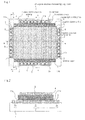
- Fig. 1 is a plan view showing an organic electroluminescent lighting device according to an embodiment of the present invention.
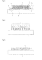
- Fig. 2 is a sectional view taken along cut line A-A shown in Fig. 1 .
- Fig. 3 is a sectional view taken along cut line B-B shown in Fig. 1 .
- Fig. 4 is a sectional view taken along cut line C-C shown in Fig. 1 .
- Fig. 5 is a sectional view taken along cut line D-D shown in Fig. 1 .
- organic light emitting layer 4 and negative electrode film 5 are not shown.
- positive electrode film 2 and negative electrode terminal film 3 are formed separate from each other on the surface of transparent substrate 1 (first film formation step).
- positive electrode film 2 includes terminal 2a and electrode 2b, and organic light emitting film 4 is formed on the surface of electrode 2b (second film formation step).
- negative electrode film 5 is formed continuously from the surface of organic light emitting film 4 to the surface of negative electrode terminal film 3 (third film formation step).
- Transparent substrate 1 is a glass substrate or a plastic substrate.
- Positive electrode film 2 is mainly made of an indium tin oxide (ITO). Terminals 2a are located at both ends of positive electrode film 2, and electrode 2b is formed to be continuous from terminal 2a. Terminal 2a can be disposed at one end of positive electrode film 2.
- ITO indium tin oxide
- negative electrode terminal film 3 includes resistive region 7 (first resistive region).
- Resistive region 7 includes a plurality of openings 6 (first openings) (refer to Fig. 1 ).
- the plurality of openings 6 is arranged vertically to the forward traveling direction of current I.
- Each of the plurality of openings 6 is surrounded with negative electrode terminal film 3, and the surface of transparent substrate 1 is exposed. Because of the inclusion of the plurality of openings 6, the cross-sectional area of conductor 12 (refer to Fig. 4 ) in resistive region 7 is smaller than that of negative electrode terminal film 3 (refer to Fig. 5 ) at boundary 11a with the outer peripheral part of negative electrode film 5.
- Negative electrode terminal film 3 accordingly serves as a resistive component.
- terminal 2a of positive electrode film 2 includes resistive region 8 (second resistive region).
- resistive region 8 includes a plurality of openings 8 (second openings) (refer to Fig. 1 ). Because of the inclusion of the plurality of openings 8, the cross-sectional area of a conductor in resistive region 8 is smaller than that of terminal 2a at boundary 11b with electrode 2b. Terminal 2a accordingly serves as a resistive component.
- the resistive component is added on the negative electrode side, and thus it is difficult for a large current to flow through negative electrode film 5. As a result, since it is difficult for negative electrode film 5 to be damaged even when inrush current flows, the occurrence of short-circuiting caused by the inrush current can be reduced.
- the resistive component is added on the positive electrode side.
- the resistive components are accordingly formed on both of the positive electrode side and the positive electrode side. This limits the inrush current in both terminal 2a and negative electrode terminal film 3, and thus the occurrence of a short circuit caused by the inrush current is further reduced. Even when static electricity momentarily generates a high electric field, since voltage drops occur in both terminal 2a and negative electrode terminal film 3, a voltage applied between positive electrode terminal 2 and negative electrode film 5 is decreased. As a result, the occurrence of insulation breakdown caused by the static electricity is further reduced.
- terminal 2a and electrode 2b are made of similar materials. This enables collective formation of openings 8 (by one mask) during the film formation step of positive electrode film 2. Accordingly, resistive region 9 can be easily formed without increasing the number of steps. Further, when positive electrode film 2 and negative electrode terminal film 3 are made of similar materials, these can be formed en bloc. As a result, resistive regions 7 and 9 can be easily formed without increasing the number of steps.
- negative electrode terminal film 3 and negative electrode film 5 can be made of different materials.
- negative electrode terminal film 3 by setting the resistance of the material of negative electrode terminal film 3 higher than that of the material of negative electrode film 5, even when no opening 6 is formed, negative electrode terminal film 3 can serve as the resistive component of the negative electrode side.
- terminal 2a and electrode 2b can be made of different materials. In this case, by setting the resistance of the material of terminal 2a higher than that of the material of electrode 2b, even when no opening 6 is formed, terminal 2a can serve as the resistive component of the positive electrode side.
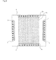
- Figs. 6 to 8 are plan views showing organic electroluminescent lighting devices according to the other embodiments of the present invention. In Figs. 6 to 8 , for easier understanding, organic light emitting layer 4 and negative electrode film 5 are not shown.
- openings 6 and 8 are formed as means for forming resistive regions 7 and 9.
- the means for forming resistive regions 7 and 9 is not limited to openings 6 and 8.
- constricted parts can be formed in terminal 2a and negative electrode terminal film 3 to be used as resistive regions 7 and 9.
- the ends of terminal 2a and negative electrode terminal film 3 can be formed into comb shapes to be used as resistive regions 7 and 9.
Landscapes
- Physics & Mathematics (AREA)
- Optics & Photonics (AREA)
- Electroluminescent Light Sources (AREA)
Applications Claiming Priority (2)
| Application Number | Priority Date | Filing Date | Title |
|---|---|---|---|
| JP2010103166 | 2010-04-28 | ||
| PCT/JP2011/060131 WO2011136205A1 (fr) | 2010-04-28 | 2011-04-26 | Dispositif d'éclairage électroluminescent organique et procédé de fabrication associé |
Publications (2)
| Publication Number | Publication Date |
|---|---|
| EP2536251A1 true EP2536251A1 (fr) | 2012-12-19 |
| EP2536251A4 EP2536251A4 (fr) | 2016-11-16 |
Family
ID=44861503
Family Applications (1)
| Application Number | Title | Priority Date | Filing Date |
|---|---|---|---|
| EP11774986.1A Withdrawn EP2536251A4 (fr) | 2010-04-28 | 2011-04-26 | Dispositif d'éclairage électroluminescent organique et procédé de fabrication associé |
Country Status (4)
| Country | Link |
|---|---|
| US (1) | US9680125B2 (fr) |
| EP (1) | EP2536251A4 (fr) |
| JP (1) | JPWO2011136205A1 (fr) |
| WO (1) | WO2011136205A1 (fr) |
Families Citing this family (7)
| Publication number | Priority date | Publication date | Assignee | Title |
|---|---|---|---|---|
| WO2013047742A1 (fr) * | 2011-09-30 | 2013-04-04 | パナソニック出光Oled照明 株式会社 | Dispositif électroluminescent planaire |
| JP2014154212A (ja) * | 2013-02-04 | 2014-08-25 | Toshiba Corp | 有機電界発光素子、照明装置及び照明システム |
| WO2015137771A1 (fr) * | 2014-03-14 | 2015-09-17 | 주식회사 엘지화학 | Dispositif électroluminescent organique |
| US20170220179A1 (en) * | 2016-01-29 | 2017-08-03 | Nanoport Technology Inc. | Cross device gesture detection |
| JP6867403B2 (ja) | 2016-11-11 | 2021-04-28 | 株式会社ホタルクス | 有機el装置 |
| JP6375015B1 (ja) | 2017-04-25 | 2018-08-15 | 住友化学株式会社 | 有機電子デバイスの製造方法 |
| JP6375016B1 (ja) * | 2017-04-26 | 2018-08-15 | 住友化学株式会社 | 電極付き基板、積層基板及び有機デバイスの製造方法 |
Family Cites Families (13)
| Publication number | Priority date | Publication date | Assignee | Title |
|---|---|---|---|---|
| JPS62170188A (ja) | 1986-01-22 | 1987-07-27 | 伊勢電子工業株式会社 | 薄膜elパネル |
| JPH0254894A (ja) | 1988-08-17 | 1990-02-23 | Sharp Corp | 薄膜el表示素子 |
| JPH02126589A (ja) | 1988-11-04 | 1990-05-15 | Sharp Corp | 薄膜elパネル |
| US6111357A (en) * | 1998-07-09 | 2000-08-29 | Eastman Kodak Company | Organic electroluminescent display panel having a cover with radiation-cured perimeter seal |
| JP2001155856A (ja) | 1998-10-30 | 2001-06-08 | Tdk Corp | 有機el表示装置 |
| JP2001085158A (ja) | 1999-09-10 | 2001-03-30 | Toyota Central Res & Dev Lab Inc | 有機電界発光素子 |
| JP2002359085A (ja) * | 2001-05-31 | 2002-12-13 | Nippon Seiki Co Ltd | 有機elパネル及びその製造方法 |
| JP2004296154A (ja) * | 2003-03-26 | 2004-10-21 | Konica Minolta Holdings Inc | 電極とその製造方法及び有機エレクトロルミネッセンス素子 |
| JP4729949B2 (ja) * | 2005-03-09 | 2011-07-20 | 株式会社豊田自動織機 | 有機エレクトロルミネッセンス素子 |
| JP4774787B2 (ja) | 2005-03-31 | 2011-09-14 | Tdk株式会社 | 表示装置 |
| JP2007227094A (ja) | 2006-02-22 | 2007-09-06 | Matsushita Electric Works Ltd | 有機el素子を用いた照明用パネルおよび照明装置 |
| KR100811473B1 (ko) | 2006-10-17 | 2008-03-07 | 엘지전자 주식회사 | 전계발광패널 및 그를 포함하는 광원장치 |
| JP5517433B2 (ja) | 2008-10-21 | 2014-06-11 | キヤノン株式会社 | リードレス電子部品の実装方法及び実装構造 |
-
2011
- 2011-04-26 JP JP2012512848A patent/JPWO2011136205A1/ja active Pending
- 2011-04-26 EP EP11774986.1A patent/EP2536251A4/fr not_active Withdrawn
- 2011-04-26 US US13/634,160 patent/US9680125B2/en not_active Expired - Fee Related
- 2011-04-26 WO PCT/JP2011/060131 patent/WO2011136205A1/fr not_active Ceased
Also Published As
| Publication number | Publication date |
|---|---|
| US9680125B2 (en) | 2017-06-13 |
| EP2536251A4 (fr) | 2016-11-16 |
| WO2011136205A1 (fr) | 2011-11-03 |
| US20130002126A1 (en) | 2013-01-03 |
| JPWO2011136205A1 (ja) | 2013-07-22 |
Similar Documents
| Publication | Publication Date | Title |
|---|---|---|
| US9680125B2 (en) | Organic electroluminescent lighting device and method for manufacturing the same | |
| EP2560462A1 (fr) | Dispositif d'éclairage électroluminescent organique | |
| CN104461189B (zh) | 触控面板 | |
| JP4451522B2 (ja) | 有機及びポリマー発光デバイスの信頼性を向上させるための構造及びその製造方法 | |
| CN107134471B (zh) | 显示装置和挠性显示装置 | |
| CN109545838B (zh) | 一种显示面板及显示装置 | |
| US20130120312A1 (en) | Touch panel | |
| KR100729046B1 (ko) | 유기 발광 표시장치의 정전기 방지 구조 및 그 제조 방법 | |
| CN102184968A (zh) | 具有单栅双沟道结构的薄膜晶体管及其制造方法 | |
| CN109950286B (zh) | 显示面板 | |
| CN103926769A (zh) | 一种阵列基板、显示面板及显示器 | |
| CN108873515A (zh) | 显示面板和显示装置 | |
| US8680767B2 (en) | Flat panel display apparatus, mother substrate for flat panel display apparatuses, method of manufacturing the flat panel display apparatus, and method of manufacturing the mother substrate | |
| EP2627156A1 (fr) | Dispositif d'éclairage électroluminescent organique et procédé de fabrication dudit dispositif d'éclairage | |
| CN110456942B (zh) | 触控显示面板和触控显示装置 | |
| CN107479285A (zh) | 一种阵列基板及显示装置 | |
| US20140048777A1 (en) | Organic light emitting diode module | |
| CN103426921B (zh) | 晶闸管元件的制造方法 | |
| US20110291118A1 (en) | Mother substrate for flat panel display apparatus and method of manufacturing the same | |
| KR101223726B1 (ko) | 평판 표시 장치, 평판 표시 장치용 원장 기판, 평판 표시 장치 제조 방법 및 평판 표시 장치용 원장 기판 제조 방법 | |
| WO2020248880A1 (fr) | Substrat de réseau et procédé de fabrication associé, et appareil d'affichage | |
| US20170005287A1 (en) | Light emitting device | |
| EP2535959A1 (fr) | Dispositif d'éclairage électroluminescent organique | |
| CN103874318B (zh) | 外围线路结构 | |
| EP4026692A1 (fr) | Capteur tactile |
Legal Events
| Date | Code | Title | Description |
|---|---|---|---|
| PUAI | Public reference made under article 153(3) epc to a published international application that has entered the european phase |
Free format text: ORIGINAL CODE: 0009012 |
|
| 17P | Request for examination filed |
Effective date: 20120912 |
|
| AK | Designated contracting states |
Kind code of ref document: A1 Designated state(s): AL AT BE BG CH CY CZ DE DK EE ES FI FR GB GR HR HU IE IS IT LI LT LU LV MC MK MT NL NO PL PT RO RS SE SI SK SM TR |
|
| DAX | Request for extension of the european patent (deleted) | ||
| RA4 | Supplementary search report drawn up and despatched (corrected) |
Effective date: 20161017 |
|
| RIC1 | Information provided on ipc code assigned before grant |
Ipc: H01L 51/52 20060101AFI20161011BHEP |
|
| STAA | Information on the status of an ep patent application or granted ep patent |
Free format text: STATUS: THE APPLICATION IS DEEMED TO BE WITHDRAWN |
|
| 18D | Application deemed to be withdrawn |
Effective date: 20170516 |