EP2538403A2 - Unipolares Grauskalenantriebsschema für Cholesterinflüssigkristallanzeigen - Google Patents
Unipolares Grauskalenantriebsschema für Cholesterinflüssigkristallanzeigen Download PDFInfo
- Publication number
- EP2538403A2 EP2538403A2 EP12184471A EP12184471A EP2538403A2 EP 2538403 A2 EP2538403 A2 EP 2538403A2 EP 12184471 A EP12184471 A EP 12184471A EP 12184471 A EP12184471 A EP 12184471A EP 2538403 A2 EP2538403 A2 EP 2538403A2
- Authority
- EP
- European Patent Office
- Prior art keywords
- voltage
- voltage signal
- row
- state
- column
- Prior art date
- Legal status (The legal status is an assumption and is not a legal conclusion. Google has not performed a legal analysis and makes no representation as to the accuracy of the status listed.)
- Withdrawn
Links
- 239000004986 Cholesteric liquid crystals (ChLC) Substances 0.000 title claims description 14
- 239000011159 matrix material Substances 0.000 claims abstract description 47
- 238000000034 method Methods 0.000 claims abstract description 31
- 230000010355 oscillation Effects 0.000 claims abstract description 8
- 230000001351 cycling effect Effects 0.000 claims abstract description 6
- 239000010410 layer Substances 0.000 description 33
- 230000001186 cumulative effect Effects 0.000 description 9
- 238000002310 reflectometry Methods 0.000 description 9
- 239000000758 substrate Substances 0.000 description 6
- 230000001419 dependent effect Effects 0.000 description 4
- 238000010586 diagram Methods 0.000 description 4
- 230000004044 response Effects 0.000 description 4
- 210000004027 cell Anatomy 0.000 description 3
- 239000000463 material Substances 0.000 description 3
- FHNINJWBTRXEBC-UHFFFAOYSA-N Sudan III Chemical compound OC1=CC=C2C=CC=CC2=C1N=NC(C=C1)=CC=C1N=NC1=CC=CC=C1 FHNINJWBTRXEBC-UHFFFAOYSA-N 0.000 description 2
- 210000002421 cell wall Anatomy 0.000 description 2
- 239000003086 colorant Substances 0.000 description 2
- 230000003247 decreasing effect Effects 0.000 description 2
- 230000005684 electric field Effects 0.000 description 2
- 230000003287 optical effect Effects 0.000 description 2
- 239000000853 adhesive Substances 0.000 description 1
- 230000001070 adhesive effect Effects 0.000 description 1
- -1 but not limited to Substances 0.000 description 1
- 239000004020 conductor Substances 0.000 description 1
- 238000002474 experimental method Methods 0.000 description 1
- 229920002457 flexible plastic Polymers 0.000 description 1
- 239000011521 glass Substances 0.000 description 1
- AMGQUBHHOARCQH-UHFFFAOYSA-N indium;oxotin Chemical compound [In].[Sn]=O AMGQUBHHOARCQH-UHFFFAOYSA-N 0.000 description 1
- 230000031700 light absorption Effects 0.000 description 1
- 239000004973 liquid crystal related substance Substances 0.000 description 1
- 230000000644 propagated effect Effects 0.000 description 1
- 239000002356 single layer Substances 0.000 description 1
Images


Classifications
-
- G—PHYSICS
- G09—EDUCATION; CRYPTOGRAPHY; DISPLAY; ADVERTISING; SEALS
- G09G—ARRANGEMENTS OR CIRCUITS FOR CONTROL OF INDICATING DEVICES USING STATIC MEANS TO PRESENT VARIABLE INFORMATION
- G09G3/00—Control arrangements or circuits, of interest only in connection with visual indicators other than cathode-ray tubes
- G09G3/20—Control arrangements or circuits, of interest only in connection with visual indicators other than cathode-ray tubes for presentation of an assembly of a number of characters, e.g. a page, by composing the assembly by combination of individual elements arranged in a matrix no fixed position being assigned to or needed to be assigned to the individual characters or partial characters
- G09G3/34—Control arrangements or circuits, of interest only in connection with visual indicators other than cathode-ray tubes for presentation of an assembly of a number of characters, e.g. a page, by composing the assembly by combination of individual elements arranged in a matrix no fixed position being assigned to or needed to be assigned to the individual characters or partial characters by control of light from an independent source
- G09G3/36—Control arrangements or circuits, of interest only in connection with visual indicators other than cathode-ray tubes for presentation of an assembly of a number of characters, e.g. a page, by composing the assembly by combination of individual elements arranged in a matrix no fixed position being assigned to or needed to be assigned to the individual characters or partial characters by control of light from an independent source using liquid crystals
- G09G3/3611—Control of matrices with row and column drivers
- G09G3/3622—Control of matrices with row and column drivers using a passive matrix
- G09G3/3629—Control of matrices with row and column drivers using a passive matrix using liquid crystals having memory effects, e.g. ferroelectric liquid crystals
-
- G—PHYSICS
- G09—EDUCATION; CRYPTOGRAPHY; DISPLAY; ADVERTISING; SEALS
- G09G—ARRANGEMENTS OR CIRCUITS FOR CONTROL OF INDICATING DEVICES USING STATIC MEANS TO PRESENT VARIABLE INFORMATION
- G09G3/00—Control arrangements or circuits, of interest only in connection with visual indicators other than cathode-ray tubes
- G09G3/20—Control arrangements or circuits, of interest only in connection with visual indicators other than cathode-ray tubes for presentation of an assembly of a number of characters, e.g. a page, by composing the assembly by combination of individual elements arranged in a matrix no fixed position being assigned to or needed to be assigned to the individual characters or partial characters
- G09G3/34—Control arrangements or circuits, of interest only in connection with visual indicators other than cathode-ray tubes for presentation of an assembly of a number of characters, e.g. a page, by composing the assembly by combination of individual elements arranged in a matrix no fixed position being assigned to or needed to be assigned to the individual characters or partial characters by control of light from an independent source
- G09G3/36—Control arrangements or circuits, of interest only in connection with visual indicators other than cathode-ray tubes for presentation of an assembly of a number of characters, e.g. a page, by composing the assembly by combination of individual elements arranged in a matrix no fixed position being assigned to or needed to be assigned to the individual characters or partial characters by control of light from an independent source using liquid crystals
-
- G—PHYSICS
- G02—OPTICS
- G02F—OPTICAL DEVICES OR ARRANGEMENTS FOR THE CONTROL OF LIGHT BY MODIFICATION OF THE OPTICAL PROPERTIES OF THE MEDIA OF THE ELEMENTS INVOLVED THEREIN; NON-LINEAR OPTICS; FREQUENCY-CHANGING OF LIGHT; OPTICAL LOGIC ELEMENTS; OPTICAL ANALOGUE/DIGITAL CONVERTERS
- G02F1/00—Devices or arrangements for the control of the intensity, colour, phase, polarisation or direction of light arriving from an independent light source, e.g. switching, gating or modulating; Non-linear optics
- G02F1/01—Devices or arrangements for the control of the intensity, colour, phase, polarisation or direction of light arriving from an independent light source, e.g. switching, gating or modulating; Non-linear optics for the control of the intensity, phase, polarisation or colour
- G02F1/13—Devices or arrangements for the control of the intensity, colour, phase, polarisation or direction of light arriving from an independent light source, e.g. switching, gating or modulating; Non-linear optics for the control of the intensity, phase, polarisation or colour based on liquid crystals, e.g. single liquid crystal display cells
- G02F1/133—Constructional arrangements; Operation of liquid crystal cells; Circuit arrangements
-
- G—PHYSICS
- G09—EDUCATION; CRYPTOGRAPHY; DISPLAY; ADVERTISING; SEALS
- G09G—ARRANGEMENTS OR CIRCUITS FOR CONTROL OF INDICATING DEVICES USING STATIC MEANS TO PRESENT VARIABLE INFORMATION
- G09G2300/00—Aspects of the constitution of display devices
- G09G2300/04—Structural and physical details of display devices
- G09G2300/0469—Details of the physics of pixel operation
- G09G2300/0478—Details of the physics of pixel operation related to liquid crystal pixels
- G09G2300/0482—Use of memory effects in nematic liquid crystals
- G09G2300/0486—Cholesteric liquid crystals, including chiral-nematic liquid crystals, with transitions between focal conic, planar, and homeotropic states
-
- G—PHYSICS
- G09—EDUCATION; CRYPTOGRAPHY; DISPLAY; ADVERTISING; SEALS
- G09G—ARRANGEMENTS OR CIRCUITS FOR CONTROL OF INDICATING DEVICES USING STATIC MEANS TO PRESENT VARIABLE INFORMATION
- G09G3/00—Control arrangements or circuits, of interest only in connection with visual indicators other than cathode-ray tubes
- G09G3/20—Control arrangements or circuits, of interest only in connection with visual indicators other than cathode-ray tubes for presentation of an assembly of a number of characters, e.g. a page, by composing the assembly by combination of individual elements arranged in a matrix no fixed position being assigned to or needed to be assigned to the individual characters or partial characters
- G09G3/2007—Display of intermediate tones
- G09G3/2011—Display of intermediate tones by amplitude modulation
-
- G—PHYSICS
- G09—EDUCATION; CRYPTOGRAPHY; DISPLAY; ADVERTISING; SEALS
- G09G—ARRANGEMENTS OR CIRCUITS FOR CONTROL OF INDICATING DEVICES USING STATIC MEANS TO PRESENT VARIABLE INFORMATION
- G09G3/00—Control arrangements or circuits, of interest only in connection with visual indicators other than cathode-ray tubes
- G09G3/20—Control arrangements or circuits, of interest only in connection with visual indicators other than cathode-ray tubes for presentation of an assembly of a number of characters, e.g. a page, by composing the assembly by combination of individual elements arranged in a matrix no fixed position being assigned to or needed to be assigned to the individual characters or partial characters
- G09G3/2007—Display of intermediate tones
- G09G3/2014—Display of intermediate tones by modulation of the duration of a single pulse during which the logic level remains constant
Definitions
- the present disclosure relates to drive schemes for passive matrix display systems. More specifically, the present disclosure relates to gray scale drive schemes for cholesteric liquid crystal display systems.
- ChLCD's Cholesteric liquid crystal displays have existed for several decades. ChLCD's are unique because of their "nonvolatile memory" characteristic; once an image is written to a display, the current image will remain indefinitely until a new image is written. ChLCD's can also be viewed in ambient light without back lighting. Both of these characteristics significantly reduce total power consumption when compared to other displays.
- ChLCD's have inherently slow refresh rates.
- drive schemes for ChLCD's have evolved significantly and have become very complex.
- Known drive schemes include bipolar and multi-phase drive schemes. Bipolar drive schemes frequently have insufficient voltage to effectively drive a ChLCD, and the complexity of both bipolar and multi-stage drive schemes results in high costs.
- One aspect of the present invention includes a method for driving at least a portion of a passive matrix display system having rows and columns forming pixels.
- the method includes initially driving the portion of the passive matrix display system to a uniform state. It also includes outputting a column voltage signal that oscillates between two non-negative voltages, where at least three different sets of non-negative voltages cause three different states of the gray scale reflectivity of the pixels.
- first row voltage signal oscillating between a non-planar voltage and a planar voltage which is applied to a row of the matrix being written includes outputting a second row voltage signal where the difference between the second row voltage signal and the column voltage signal at any time is sufficiently low that a state of a pixel receiving the voltage signal will remain substantially unchanged and that is applied to all rows of the matrix not currently being written.
- Another aspect of the present disclosure includes a system for driving a display using the described method and including a column driver for outputting column voltage signals and a row driver for outputting row voltage signals.
- Another aspect of the present disclosure includes a system for driving a display using the above described method and also including a passive matrix display, a column driver for outputting column voltage signals, a row driver for outputting row voltage signals, and a controller, electrically coupled to the display and column and row drivers, which controls the column and row voltage signals.
- Another aspect of the present disclosure includes a method for driving at least a portion of a passive matrix display system having rows and columns forming pixels.
- the method includes initially driving the portion of the passive matrix display system to a uniform state. It also includes outputting a column voltage signal, cycling through four non-negative voltage levels, wherein the first voltage level is sufficiently high to change the pixel state to a planar reflective state, the second voltage will put the pixel into a weakly scattering focal conic state, the third voltage is sufficiently low that it cannot substantially change the pixel state, and the fourth voltage is the difference between the first voltage and the second voltage.
- the parameter N is a total number of desired levels of gray scale
- the parameter n is a number representing a particular desired level of gray scale within the range of 0 to N -1.
- Drive period is a length of time inversely proportional to a frequency of oscillation of the row voltages.
- the method also includes outputting a first row voltage signal oscillating between a non-planar voltage and a planar voltage that is applied to a row of the matrix being written.
- Another aspect of the present disclosure includes a system for driving a display using the above described method and also including a passive matrix display, a column driver for outputting column voltage signals, a row driver for outputting row voltage signals, and a controller electronically coupled to the display and column and row drivers which controls the column and row voltage signals.
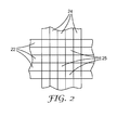
- the current disclosure includes a passive matrix display, which may be, for example, a cholesteric liquid crystal display as shown in FIG. 1 .
- a passive matrix display which may be, for example, a cholesteric liquid crystal display as shown in FIG. 1 .
- An exemplary ChLCD is described in United States Patent No. 5,453,863 , incorporated herein by reference as if fully set forth. Alternatively, other types of passive matrix displays may be used.
- the exemplary ChLCD module shown in FIG. 1 contains three active layers 17, 18, 19. The active layers can correspond with the colors red 17, green 18 and blue 19, and each layer can be addressed by its own pair of indium-tin oxide (ITO) electrodes 16.
- ITO indium-tin oxide
- a display may contain fewer active layers or more active layers. For example, a display may contain multiple active layers for certain colors or additional contrast layers.
- each active layer 17, 18, 19 can include a matrix of rows 22 and columns 24 forming pixels 25 that can be controlled individually.
- Active layers 17, 18, 19 of ChLCD's are typically composed of a chiral nematic liquid crystal material and a cell wall structure. The cell wall structure and the liquid crystal cooperate to form focal conic and twisted planar textures.
- Such cells have multiple stable optical states characterized by varying degrees of intensity of reflection. Cells can be driven from one state to another using an electric field. The optical state of the material can be changed to a new stable state to reflect any desired level of reflection along a continuum of such states, thus creating a "gray scale.” After the electric field is removed, the current state will remain indefinitely.
- a layer of substrate 12 can be disposed on each side of the active layers for a total of six layers of substrate 12 within the display stack. Alternatively, for example, a single layer of substrate 12 can be disposed between active layers and on each end of the stack for a total of four layers of substrate 12. Any number of substrate layers 12 can be arranged in any suitable manner. Active layers 17, 18, 19, each surrounded by a conductor 16 and substrate 12, can then be joined with a total of two layers of adhesive 14 to create a full color ChLCD.
- An exemplary display 1 may also have a background layer 11. The background layer 11 absorbs light not reflected or scattered by the active layers. The background layer may be black, or alternatively, it may be any other color appropriate for light absorption.
- a display 1 can be enclosed in any suitable material including, but not limited to, glass or flexible plastic.
- FIG. 3 shows a block diagram of an exemplary system for driving a display 1 consistent with the present disclosure.
- Each active layer of the display 1 can be driven by both a column driver 2 and a row driver 4.
- the column driver 2 and row driver 4 can include a single electronic device or two or more electronic devices.
- the HV633PG, a 32-channel 128-level display driver manufactured by Supertex, Inc. can be used.
- Each driver 2, 4 can be powered by a bias voltage supply 10.
- the bias voltage supply 10 can be monitored by the controller 6 and powered by a power source 9, which also provides power to the controller 6.
- the controller 6 could be a PIC microcontroller made by Microchip Technology, Inc.
- Alternative power, voltage, controller and driver configurations consistent with the present disclosure will be apparent to individuals skilled in the art.
- the controller 6 When writing a desired image to a display 1, the controller 6 receives input data 7 from an outside source, for example, a user interface, regarding what image or images should be displayed. The controller 6 then accesses the associated image data stored in RAM 8. Using this information, the controller transmits data to the column driver 2 and row driver 4 indicating what signal should be applied to each row and each column of the display, along with the appropriate number of periods over which the signal should be transmitted.
- the display can be floated at a constant positive voltage level to allow an AC voltage signal to range from zero or some lower positive voltage to a higher voltage.
- FIG. 4 illustrates a response of a pixel in an active layer to varying voltage levels. Examples of appropriate ranges for voltage levels are in Table 1 below. Table 1: Voltage levels and corresponding example ranges. Voltage Level Example Range V1 3 - 10 V V2 5 - 10 V V3 10 - 25 V V4 20 - 31 V V5 10 - 31 V V6 20 - 40 V
- the response of a pixel to a given voltage level is dependent on the initial pixel state.
- a pixel is initially in a planar reflective state 41
- application of a sufficiently low voltage to the cell, less than V1 will not substantially change the state of the pixel.
- a planar reflective state 41 results in substantially the highest level of reflection for a given pixel.
- the resulting reflective state 43 is gray scale and is dependent upon, but not linearly related to, the precise level of voltage applied.
- a pixel in a focal conic state 42 has a very low level of reflection. Instead, the pixel scatters light, resulting in a black appearance.
- Each pixel 25 in a display receives a row voltage signal and a column voltage signal simultaneously.
- the row voltage signal and column voltage signal correspond to the row 22 and column 24 which intersect at the location of the pixel 25.
- the total voltage applied to a pixel at any given point in time is the difference between the row voltage signal and column voltage signal that intersect at that pixel.
- all pixels contained in the display can be initially driven to a uniform state, for example, a planar reflective state. Driving pixels to an initial uniform state can result in a more uniform and higher contrast appearance of the subsequently displayed image.
- the desired image is then written to the display by changing each pixel in each active layer to the desired level of reflectivity.
- column voltage signals can primarily control the level of reflectivity while row voltage signals can control which row is being written at any given time.
- row voltage signals could primarily control the level of reflectivity while column voltage signals could control which column is being written at any given time.
- Voltage levels V1, V2, V3, V4, V5 and V6 may vary with each individual active layer in a display.
- the key voltage levels to be determined for each state are V3, which will drive a pixel to a focal conic state, and V4, which will drive a pixel to a planar state.
- Exemplary voltages used for active layers 17, 18, 19 shown in FIG. 1 are shown in Table 2 below. Table 2: Example voltage levels for various active display layers. Active Layer V3 V4 Red 17 18 V 23 V Green 18 20 V 26 V Blue 19 24 V 30 V
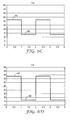
- FIGS. 5A - 5B show exemplary row voltage signals for configurations using either amplitude modulation or pulse width modulation.
- Vselect the voltage signal illustrated in FIG. 5A can be transmitted to a row currently being written.
- the minimum voltage level 51 is approximately equal to zero and the maximum voltage level 52 is approximately equal to V4 shown in FIG. 4 .
- row voltage levels 51, 52 can be increased or decreased. If a row voltage level 51, 52 is increased or decreased, the voltage that the display is floated at should also be adjusted so that it remains at the center voltage between minimum 51 and maximum 52.
- FIG. 5B illustrates a voltage signal that can be transmitted to all rows not being written at any given time.
- Vnonselect the voltage signal shown in FIG.
- the maximum voltage level 53 is approximately equal to the sum of V4 and V3 divided by two ((V4+V3)/2).
- the minimum voltage level 54 is approximately equal to the difference between V4 and V3 divided by two ((V4-V3)/2).
- Exemplary row voltage signals in FIG. 5A - 5B are shown over two periods.
- the length of a period can vary.
- An exemplary period may be 0.01 seconds, or as long as about 0.02 seconds or longer, or as short as about 0.002 seconds or shorter.
- the frequency of oscillation for a row voltage signal such as those shown in FIGS. 5A - 5B is inversely related to the period.
- exemplary frequency may be about 100 Hz, or as low as about 50 Hz or lower, or as high as about 500 Hz or higher.
- FIGS. 6A - 6D show exemplary column voltage signals for use in an amplitude modulation driving method. These column voltage signals can be used in conjunction with row signals such as the exemplary signals illustrated in FIG. 5A - 5B . Row voltage signals and column voltage signals should have the same frequency and period.
- the column voltage signal illustrated in FIG. 6A can change a pixel's state to planar reflective.
- the maximum voltage level 61 is approximately equal to V4, and the minimum voltage level 62 is approximately zero.
- the column voltage signal shown in FIG. 6A is approximately in-phase with the row voltage signal shown in FIG. 5B .
- the pixel in that column receiving a row voltage signal as illustrated in FIG. 5A will receive a cumulative voltage signal alternating between negative and positive V4, and will be changed to a planar reflective state.
- Pixels receiving a row voltage signal as shown in FIG. 5B will receive a cumulative voltage signal alternating between the negative and positive of the difference between V3 and V4 divided by two ((V3-V4)/2).
- ChLCD displays that have the following characteristic: V1 is greater than or equal to the difference between V4 and V3 divided by two ((V4-V3)/2).
- the column voltage signal illustrated in FIG. 6B can change a pixel's state to focal conic.
- the maximum voltage level 63 is approximately equal to V3 and the minimum voltage level 64 is approximately equal to the difference between V4 and V3.
- the pixel in that column receiving a row voltage signal as illustrated in FIG. 5A will receive a cumulative voltage signal alternating between positive and negative V3, a voltage level sufficient to drive the pixel state to focal conic.
- the pixels in that column receiving a row voltage signal as illustrated in FIG. 5B will receive a cumulative voltage signal alternating between the positive and the negative of the difference between V4 and V3 divided by two ((V4-V3)/2). Because this signal is less than or equal to V1, the state of the pixels receiving this signal will not change.
- the column voltage signal illustrated in FIG. 6C can change a pixel's state to 25% of the reflection of a planar reflective level.
- the maximum voltage level 65 was determined by experimentally characterizing the response of a pixel to differing voltage levels and using this information to find the necessary column voltage based on row voltage levels to achieve the desired level of reflectivity. Maximum voltage level 65 was then hardwired into the controller. The minimum voltage level 66 can be determined and hardwired in the same manner.
- the column voltage signal illustrated in FIG. 6D can change a pixel's state to 75% of the reflection of a planar voltage.
- Maximum and minimum voltage levels 67, 68 can be found using the same method used to find maximum and minimum voltage levels 65,66.
- FIGS. 6A - 6D show voltage signals that can be used to achieve four gray scale shades
- any number of shades can be achieved using experimental methods to determine minimum 66, 68 and maximum 65, 67 voltage levels.
- shades can have any variety of levels and increments.
- a four shade gray scale system can have shades for a focal conic state, thirty-three percent reflection of a planar voltage, sixty-six percent reflection of a planar voltage, and a planar reflective state.
- a drive system consistent with the present disclosure can also use pulse width modulation to generate column voltage signals as illustrated in FIGS. 7A - 7C .
- the exemplary column voltage signals shown in FIGS. 7A - 7C can be used in combination with row voltage signals such as the exemplary signals shown in FIGS. 5A - 5B .
- Row voltage signals and column voltage signals must have the same frequency and period.
- the column voltage signal illustrated in FIG. 7A can change a pixel's state to planar reflective.
- the maximum voltage level 71 is approximately equal to or greater than V4, and the minimum voltage level 72 is approximately zero.
- the column voltage signal shown in FIG. 7A is approximately in-phase with the row voltage signal shown in FIG. 5B .
- the pixel in that column receiving a row voltage signal as illustrated in FIG. 5A will receive a cumulative voltage signal alternating between negative and positive V4, and will be changed to a planar reflective state regardless of thc pixel's initial state.
- Pixels receiving a row voltage signal as shown in FIG. 5B receive a cumulative voltage signal alternating between the negative and positive of the difference between V3 and V4 divided by two ((V3-V4)/2).
- the column voltage signal illustrated in FIG. 7B can change a pixel's state to focal conic.
- the maximum voltage level 73 is approximately equal to V3 and the minimum voltage level 74 is approximately equal to the difference between V4 and V3.
- the pixel in that column receiving a row voltage signal as illustrated in FIG. 5A receives a cumulative voltage signal alternating between positive and negative V3, a voltage level sufficient to drive the pixel state to focal conic.
- the pixels in that column receiving a row voltage signal such as illustrated in FIG. 5B will receive a cumulative voltage signal alternating between the positive and the negative of the difference between V4 and V3 divided by two ((V4-V3)/2). Because this signal is less than or equal to V1, the state of the pixels receiving this signal will not change.
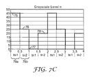
- the column voltage signal illustrated in FIG. 7C can drive a pixel to a desired level of gray scale, n , within a range of 0 to N-1 levels, where N is the total number of desired levels of gray scale.
- the signal shown in FIG. 7C extends over two periods, and each period is broken into four time segments, two of each of t1 69a and t2 69b.
- the exemplary signal in FIG. 7C cycles through four voltage levels during each period.
- the first voltage level 75 can have a time period of tn1 and is approximately equal to or greater than V4. Voltage level 75 is sufficiently high to change a pixel to a planar reflective state.
- the second voltage level 76 can have a time period of t2 and is approximately equal to V3.
- Voltage level 76 can change a pixel state to a weakly scattering focal conic state.
- the third voltage level 77 can be 0V and is sufficiently low that it cannot substantially change a pixel state.
- the fourth voltage level 78 is the difference between the first voltage level 75 and the second voltage level 76.
- first voltage level 75 and third voltage level 77 should still have corresponding time periods of length t1 and a second voltage level 76 and fourth voltage level 78 should still have corresponding time periods of length t2 .
- Any desired number of shades of gray scale can be achieved by choosing a corresponding value for N .
- Shades of gray scale, n ranging from 0 to N -1 are equally spaced.
- a signal can be repeated over any desired number of periods to write a pixel.
- a signal can be repeated over approximately four periods to achieve a high level of contrast and uniformity.
Landscapes
- Physics & Mathematics (AREA)
- Engineering & Computer Science (AREA)
- General Physics & Mathematics (AREA)
- Crystallography & Structural Chemistry (AREA)
- Chemical & Material Sciences (AREA)
- Theoretical Computer Science (AREA)
- Computer Hardware Design (AREA)
- Nonlinear Science (AREA)
- Mathematical Physics (AREA)
- Optics & Photonics (AREA)
- Control Of Indicators Other Than Cathode Ray Tubes (AREA)
- Liquid Crystal (AREA)
- Liquid Crystal Display Device Control (AREA)
Applications Claiming Priority (2)
| Application Number | Priority Date | Filing Date | Title |
|---|---|---|---|
| US12/236,941 US8269801B2 (en) | 2008-09-24 | 2008-09-24 | Unipolar gray scale drive scheme for cholesteric liquid crystal displays |
| EP09816701A EP2340533A4 (de) | 2008-09-24 | 2009-09-15 | Unipolares graustufenansteuerschema für cholesterische flüssigkristallanzeigen |
Related Parent Applications (1)
| Application Number | Title | Priority Date | Filing Date |
|---|---|---|---|
| EP09816701.8 Division | 2009-09-15 |
Publications (2)
| Publication Number | Publication Date |
|---|---|
| EP2538403A2 true EP2538403A2 (de) | 2012-12-26 |
| EP2538403A3 EP2538403A3 (de) | 2013-01-09 |
Family
ID=42037186
Family Applications (2)
| Application Number | Title | Priority Date | Filing Date |
|---|---|---|---|
| EP09816701A Withdrawn EP2340533A4 (de) | 2008-09-24 | 2009-09-15 | Unipolares graustufenansteuerschema für cholesterische flüssigkristallanzeigen |
| EP12184471A Withdrawn EP2538403A3 (de) | 2008-09-24 | 2009-09-15 | Unipolares Grauskalenantriebsschema für Cholesterinflüssigkristallanzeigen |
Family Applications Before (1)
| Application Number | Title | Priority Date | Filing Date |
|---|---|---|---|
| EP09816701A Withdrawn EP2340533A4 (de) | 2008-09-24 | 2009-09-15 | Unipolares graustufenansteuerschema für cholesterische flüssigkristallanzeigen |
Country Status (7)
| Country | Link |
|---|---|
| US (1) | US8269801B2 (de) |
| EP (2) | EP2340533A4 (de) |
| JP (1) | JP2012503795A (de) |
| KR (1) | KR20110057251A (de) |
| CN (1) | CN102160110B (de) |
| TW (1) | TW201023163A (de) |
| WO (1) | WO2010036531A2 (de) |
Families Citing this family (5)
| Publication number | Priority date | Publication date | Assignee | Title |
|---|---|---|---|---|
| GB0512829D0 (en) * | 2005-06-23 | 2005-08-03 | Magink Display Technologies | Video drive scheme for a cholesteric liquid crystal display device |
| US8599353B2 (en) | 2010-05-28 | 2013-12-03 | 3M Innovative Properties Company | Display comprising a plurality of substrates and a plurality of display materials disposed between the plurality of substrates that are connected to a plurality of non-overlapping integral conductive tabs |
| TWI423215B (zh) * | 2010-11-10 | 2014-01-11 | Au Optronics Corp | 雙穩態顯示器之驅動方法 |
| TWI535283B (zh) * | 2013-08-29 | 2016-05-21 | 台達電子工業股份有限公司 | 灰階控制方法及光學投影系統 |
| TWI612280B (zh) * | 2016-04-26 | 2018-01-21 | 磁性浮子式液面計用刻度結構 |
Citations (1)
| Publication number | Priority date | Publication date | Assignee | Title |
|---|---|---|---|---|
| US5453863A (en) | 1991-05-02 | 1995-09-26 | Kent State University | Multistable chiral nematic displays |
Family Cites Families (30)
| Publication number | Priority date | Publication date | Assignee | Title |
|---|---|---|---|---|
| CH617281A5 (de) * | 1977-07-29 | 1980-05-14 | Bbc Brown Boveri & Cie | |
| US4386350A (en) * | 1979-06-26 | 1983-05-31 | Nippon Electric Co., Ltd. | Display apparatus |
| US4890902A (en) * | 1985-09-17 | 1990-01-02 | Kent State University | Liquid crystal light modulating materials with selectable viewing angles |
| ATE178645T1 (de) * | 1991-05-02 | 1999-04-15 | Univ Kent State Ohio | Flüssigkristall lichtmodulierungs-vorrichtung und -material |
| US5644330A (en) * | 1994-08-11 | 1997-07-01 | Kent Displays, Inc. | Driving method for polymer stabilized and polymer free liquid crystal displays |
| US5748277A (en) * | 1995-02-17 | 1998-05-05 | Kent State University | Dynamic drive method and apparatus for a bistable liquid crystal display |
| US6154190A (en) * | 1995-02-17 | 2000-11-28 | Kent State University | Dynamic drive methods and apparatus for a bistable liquid crystal display |
| US5933203A (en) * | 1997-01-08 | 1999-08-03 | Advanced Display Systems, Inc. | Apparatus for and method of driving a cholesteric liquid crystal flat panel display |
| US6034752A (en) * | 1997-03-22 | 2000-03-07 | Kent Displays Incorporated | Display device reflecting visible and infrared radiation |
| AU6418098A (en) * | 1997-03-25 | 1998-10-20 | Vision - View Technologies Ltd. | Modular front-lit display panel |
| US6268840B1 (en) * | 1997-05-12 | 2001-07-31 | Kent Displays Incorporated | Unipolar waveform drive method and apparatus for a bistable liquid crystal display |
| US6133895A (en) * | 1997-06-04 | 2000-10-17 | Kent Displays Incorporated | Cumulative drive scheme and method for a liquid crystal display |
| GB9904704D0 (en) * | 1999-03-03 | 1999-04-21 | Secr Defence | Addressing bistable nematic liquid crystal devices |
| WO2001008130A1 (en) | 1999-07-21 | 2001-02-01 | Koninklijke Philips Electronics N.V. | Unipolar driving of bistable cholesteric liquid crystal display |
| AU2001231255A1 (en) * | 2000-01-31 | 2001-08-07 | Three-Five Systems, Inc. | Methods and apparatus for driving a display |
| JP2001281632A (ja) * | 2000-03-30 | 2001-10-10 | Minolta Co Ltd | 液晶表示素子の駆動方法及び液晶表示装置 |
| GB0022055D0 (en) * | 2000-09-07 | 2000-10-25 | Secr Defence | Addressing multistable nematic liquid crystal devices |
| US6710760B1 (en) * | 2000-11-28 | 2004-03-23 | Eastman Kodak Company | Unipolar drive for cholesteric liquid crystal displays |
| US6816227B2 (en) * | 2001-08-07 | 2004-11-09 | Eastman Kodak Company | Gray scale and color cholesteric liquid crystal displays |
| US7307608B2 (en) * | 2002-03-08 | 2007-12-11 | Industrial Technology Research Institute | Unipolar drive chip for cholesteric liquid crystal displays |
| US6894668B2 (en) * | 2002-05-03 | 2005-05-17 | Eastman Kodak Company | General 2 voltage levels driving scheme for cholesterical liquid crystal displays |
| JP2003344821A (ja) * | 2002-05-30 | 2003-12-03 | Nanox Corp | 液晶表示装置 |
| JP3688704B2 (ja) | 2002-09-27 | 2005-08-31 | ナノックス株式会社 | コレステリック液晶表示装置およびコレステリック液晶表示素子の駆動方法 |
| US6961036B2 (en) | 2003-01-29 | 2005-11-01 | Himax Technologies, Inc. | Single polar driving method for cholesteric liquid crystal displays |
| US7193767B1 (en) * | 2004-03-03 | 2007-03-20 | Jonathan Peeri | Method for enhancing visibility |
| US7432899B2 (en) * | 2004-05-14 | 2008-10-07 | Industrial Technology Research Institute | Driving scheme for cholesteric liquid crystal display |
| WO2006051273A1 (en) * | 2004-11-10 | 2006-05-18 | Magink Display Tecnologies Ltd. | Drive scheme for a cholesteric liquid crystal display device |
| WO2006087814A1 (ja) | 2005-02-21 | 2006-08-24 | Fujitsu Limited | 液晶表示素子 |
| JP5071388B2 (ja) | 2006-08-23 | 2012-11-14 | 富士通株式会社 | 液晶表示素子及びその駆動方法並びにそれを備えた電子ペーパー |
| JP5163652B2 (ja) * | 2007-10-15 | 2013-03-13 | 富士通株式会社 | ドットマトリクス型の表示素子を有する表示装置およびその駆動方法 |
-
2008
- 2008-09-24 US US12/236,941 patent/US8269801B2/en not_active Expired - Fee Related
-
2009
- 2009-09-15 EP EP09816701A patent/EP2340533A4/de not_active Withdrawn
- 2009-09-15 EP EP12184471A patent/EP2538403A3/de not_active Withdrawn
- 2009-09-15 JP JP2011529104A patent/JP2012503795A/ja not_active Ceased
- 2009-09-15 CN CN200980137172.0A patent/CN102160110B/zh not_active Expired - Fee Related
- 2009-09-15 KR KR1020117008960A patent/KR20110057251A/ko not_active Withdrawn
- 2009-09-15 WO PCT/US2009/056876 patent/WO2010036531A2/en not_active Ceased
- 2009-09-23 TW TW098132114A patent/TW201023163A/zh unknown
Patent Citations (1)
| Publication number | Priority date | Publication date | Assignee | Title |
|---|---|---|---|---|
| US5453863A (en) | 1991-05-02 | 1995-09-26 | Kent State University | Multistable chiral nematic displays |
Also Published As
| Publication number | Publication date |
|---|---|
| CN102160110A (zh) | 2011-08-17 |
| CN102160110B (zh) | 2014-11-05 |
| EP2340533A2 (de) | 2011-07-06 |
| EP2538403A3 (de) | 2013-01-09 |
| JP2012503795A (ja) | 2012-02-09 |
| TW201023163A (en) | 2010-06-16 |
| US8269801B2 (en) | 2012-09-18 |
| KR20110057251A (ko) | 2011-05-31 |
| US20100073405A1 (en) | 2010-03-25 |
| WO2010036531A2 (en) | 2010-04-01 |
| EP2340533A4 (de) | 2012-03-21 |
| WO2010036531A3 (en) | 2010-06-17 |
Similar Documents
| Publication | Publication Date | Title |
|---|---|---|
| EP0954841B1 (de) | Dynamische antriebsverfahren und gerät für eine bistabile flüssigkristallanzeige | |
| US8144091B2 (en) | Liquid crystal display element, driving method of the same, and electronic paper having the same | |
| US6784968B1 (en) | Addressing bistable nematic liquid crystal devices | |
| EP2538403A2 (de) | Unipolares Grauskalenantriebsschema für Cholesterinflüssigkristallanzeigen | |
| JP5148048B2 (ja) | 双安定ネマチック液晶ディスプレイ装置およびこのような装置の制御方法 | |
| JP4313702B2 (ja) | 液晶表示素子およびその駆動方法 | |
| JP5620493B2 (ja) | 大面積コレステリックディスプレイの迅速な移行 | |
| US20110221787A1 (en) | Method of driving display panel and display apparatus for performing the same | |
| US20060145993A1 (en) | Cholesteric liquid crystal display apparatus and method for driving cholesteric liquid crystal display device | |
| US8872860B2 (en) | Display device and driving method thereof | |
| JP3714324B2 (ja) | 液晶表示装置 | |
| JP3818273B2 (ja) | 液晶表示素子の駆動方法及び液晶表示装置 | |
| KR101698603B1 (ko) | 액정표시장치 및 그 구동방법 | |
| JP2004309732A (ja) | 液晶表示装置の駆動方法 | |
| JP4116029B2 (ja) | コレステリック液晶表示装置およびコレステリック液晶表示素子の駆動方法 | |
| JP2001330814A (ja) | 液晶表示装置及び液晶表示素子の駆動方法 | |
| JP2004118103A (ja) | 透明表示装置の駆動方法 | |
| JP2004171016A (ja) | 液晶表示装置 | |
| JPH10186308A (ja) | 液晶表示装置およびその液晶セルの駆動方法 | |
| JPH10186321A (ja) | 液晶表示装置およびその液晶セルの駆動方法 |
Legal Events
| Date | Code | Title | Description |
|---|---|---|---|
| PUAL | Search report despatched |
Free format text: ORIGINAL CODE: 0009013 |
|
| PUAI | Public reference made under article 153(3) epc to a published international application that has entered the european phase |
Free format text: ORIGINAL CODE: 0009012 |
|
| AC | Divisional application: reference to earlier application |
Ref document number: 2340533 Country of ref document: EP Kind code of ref document: P |
|
| AK | Designated contracting states |
Kind code of ref document: A2 Designated state(s): AT BE BG CH CY CZ DE DK EE ES FI FR GB GR HR HU IE IS IT LI LT LU LV MC MK MT NL NO PL PT RO SE SI SK SM TR |
|
| AK | Designated contracting states |
Kind code of ref document: A3 Designated state(s): AT BE BG CH CY CZ DE DK EE ES FI FR GB GR HR HU IE IS IT LI LT LU LV MC MK MT NL NO PL PT RO SE SI SK SM TR |
|
| RIC1 | Information provided on ipc code assigned before grant |
Ipc: G09G 3/36 20060101AFI20121203BHEP Ipc: G02F 1/133 20060101ALI20121203BHEP |
|
| RIN1 | Information on inventor provided before grant (corrected) |
Inventor name: CAMPBELL, PATRICK M. |
|
| STAA | Information on the status of an ep patent application or granted ep patent |
Free format text: STATUS: THE APPLICATION IS DEEMED TO BE WITHDRAWN |
|
| 18D | Application deemed to be withdrawn |
Effective date: 20130710 |