EP2538432A2 - Appareil de traitement par plasma - Google Patents
Appareil de traitement par plasma Download PDFInfo
- Publication number
- EP2538432A2 EP2538432A2 EP12165316A EP12165316A EP2538432A2 EP 2538432 A2 EP2538432 A2 EP 2538432A2 EP 12165316 A EP12165316 A EP 12165316A EP 12165316 A EP12165316 A EP 12165316A EP 2538432 A2 EP2538432 A2 EP 2538432A2
- Authority
- EP
- European Patent Office
- Prior art keywords
- antenna
- plasma
- interval
- return conductors
- high frequency
- Prior art date
- Legal status (The legal status is an assumption and is not a legal conclusion. Google has not performed a legal analysis and makes no representation as to the accuracy of the status listed.)
- Withdrawn
Links
Images




Classifications
-
- H—ELECTRICITY
- H01—ELECTRIC ELEMENTS
- H01J—ELECTRIC DISCHARGE TUBES OR DISCHARGE LAMPS
- H01J37/00—Discharge tubes with provision for introducing objects or material to be exposed to the discharge, e.g. for the purpose of examination or processing thereof
- H01J37/32—Gas-filled discharge tubes
- H01J37/32009—Arrangements for generation of plasma specially adapted for examination or treatment of objects, e.g. plasma sources
- H01J37/32082—Radio frequency generated discharge
- H01J37/321—Radio frequency generated discharge the radio frequency energy being inductively coupled to the plasma
-
- H—ELECTRICITY
- H05—ELECTRIC TECHNIQUES NOT OTHERWISE PROVIDED FOR
- H05H—PLASMA TECHNIQUE; PRODUCTION OF ACCELERATED ELECTRICALLY-CHARGED PARTICLES OR OF NEUTRONS; PRODUCTION OR ACCELERATION OF NEUTRAL MOLECULAR OR ATOMIC BEAMS
- H05H1/00—Generating plasma; Handling plasma
- H05H1/24—Generating plasma
- H05H1/46—Generating plasma using applied electromagnetic fields, e.g. high frequency or microwave energy
-
- C—CHEMISTRY; METALLURGY
- C23—COATING METALLIC MATERIAL; COATING MATERIAL WITH METALLIC MATERIAL; CHEMICAL SURFACE TREATMENT; DIFFUSION TREATMENT OF METALLIC MATERIAL; COATING BY VACUUM EVAPORATION, BY SPUTTERING, BY ION IMPLANTATION OR BY CHEMICAL VAPOUR DEPOSITION, IN GENERAL; INHIBITING CORROSION OF METALLIC MATERIAL OR INCRUSTATION IN GENERAL
- C23C—COATING METALLIC MATERIAL; COATING MATERIAL WITH METALLIC MATERIAL; SURFACE TREATMENT OF METALLIC MATERIAL BY DIFFUSION INTO THE SURFACE, BY CHEMICAL CONVERSION OR SUBSTITUTION; COATING BY VACUUM EVAPORATION, BY SPUTTERING, BY ION IMPLANTATION OR BY CHEMICAL VAPOUR DEPOSITION, IN GENERAL
- C23C16/00—Chemical coating by decomposition of gaseous compounds, without leaving reaction products of surface material in the coating, i.e. chemical vapour deposition [CVD] processes
- C23C16/44—Chemical coating by decomposition of gaseous compounds, without leaving reaction products of surface material in the coating, i.e. chemical vapour deposition [CVD] processes characterised by the method of coating
- C23C16/50—Chemical coating by decomposition of gaseous compounds, without leaving reaction products of surface material in the coating, i.e. chemical vapour deposition [CVD] processes characterised by the method of coating using electric discharges
- C23C16/505—Chemical coating by decomposition of gaseous compounds, without leaving reaction products of surface material in the coating, i.e. chemical vapour deposition [CVD] processes characterised by the method of coating using electric discharges using radio frequency discharges
- C23C16/507—Chemical coating by decomposition of gaseous compounds, without leaving reaction products of surface material in the coating, i.e. chemical vapour deposition [CVD] processes characterised by the method of coating using electric discharges using radio frequency discharges using external electrodes, e.g. in tunnel type reactors
-
- H—ELECTRICITY
- H01—ELECTRIC ELEMENTS
- H01J—ELECTRIC DISCHARGE TUBES OR DISCHARGE LAMPS
- H01J37/00—Discharge tubes with provision for introducing objects or material to be exposed to the discharge, e.g. for the purpose of examination or processing thereof
- H01J37/32—Gas-filled discharge tubes
- H01J37/32009—Arrangements for generation of plasma specially adapted for examination or treatment of objects, e.g. plasma sources
- H01J37/32082—Radio frequency generated discharge
- H01J37/321—Radio frequency generated discharge the radio frequency energy being inductively coupled to the plasma
- H01J37/3211—Antennas, e.g. particular shapes of coils
-
- H—ELECTRICITY
- H10—SEMICONDUCTOR DEVICES; ELECTRIC SOLID-STATE DEVICES NOT OTHERWISE PROVIDED FOR
- H10P—GENERIC PROCESSES OR APPARATUS FOR THE MANUFACTURE OR TREATMENT OF DEVICES COVERED BY CLASS H10
- H10P50/00—Etching of wafers, substrates or parts of devices
- H10P50/20—Dry etching; Plasma etching; Reactive-ion etching
- H10P50/24—Dry etching; Plasma etching; Reactive-ion etching of semiconductor materials
- H10P50/242—Dry etching; Plasma etching; Reactive-ion etching of semiconductor materials of Group IV materials
Definitions
- the present invention relates to a plasma processing apparatus, and more particularly, to an inductively-coupled-plasma (ICP) type plasma processing apparatus.
- ICP inductively-coupled-plasma
- Plasma processing apparatuses using high frequency (HF) to generate plasma can be categorized into capacitively-coupled-plasma (CCP) type plasma processing apparatuses capable of generating capacitively-coupled plasma and inductively-coupled-plasma type (ICP) plasma processing apparatuses capable of generating inductively-coupled plasma.
- CCP capacitively-coupled-plasma
- ICP inductively-coupled-plasma type
- ICP type plasma processing apparatuses an induction electric field generated by applying a radiofrequency current to flow to an antenna is used to generate plasma.
- the ICP plasma processing apparatuses have the advantage of being capable to lower the plasma potential.
- a flat-board-like antenna is mounted on an opening of a vacuum container through an insulating frame.
- a high frequency power supply is supplied to the flat-board-like antenna so that a high frequency current can flow from one end to the other end of the antenna, and thereby plasma is generated due to the induced electric field. It has been described in WO 2009/142016 that the plasma is used to perform a plasma treatment to the substrate in the plasma processing apparatus.
- the antenna has to be long and the impedance (particularly inductance) of the antenna increases for a large substrate; thus, a large potential difference between the two terminals of the antenna would be induced.
- the antenna potential is influenced by the plasma potential via the capacitance of the plasma, the antenna potential is increased with an increase of the plasma potential.
- one exemplary embodiment of the present invention is to provide an (inductively-coupled plasma) ICP type plasma processing apparatus capable of decreasing the effective inductance of the antenna and suppressing the plasma potential, and moreover the plasma density distribution in the longitudinal direction of the antenna can further be controlled.
- the plasma processing apparatus of the present invention is an ICP type.
- a high frequency current is applied to an antenna that is substantially straight in a plan view of the antenna so that an electric field is induced in a vacuum container to generate plasma for performing a plasma treatment to a substrate.
- the antenna is constructed by two go-and-return conductors closely disposed to each other in a perpendicular line direction, which stands on a surface of the substrate, i.e., the direction is perpendicular to the surface of the substrate.
- the high frequency current can flow in opposite directions between the go-and-return inductors.
- the interval formed in the direction between the two go-and-return conductors can be changed in the longitudinal direction of the antenna, i.e., the interval between the two go-and-return conductors is different in the longitudinal direction of the antenna.
- the perpendicular line direction that stands on the surface of the substrate is called an up-down direction and the direction intersecting the perpendicular line is called a left-right direction in this specification. Accordingly, the up-down direction is not necessarily the vertical direction.
- the effective inductance of the antenna is decreased due to the mutual inductance between the two go-and-return conductors. Accordingly, antenna potential can be decreased and thus the plasma potential can be decreased.
- the mutual inductance between the two go-and-return conductors can be varied in the longitudinal direction of the antenna by varying the interval in the up-down direction of the two go-and-return conductors to be different in the longitudinal direction of the antenna, the electromagnetic energy supplied for plasma from the antenna can be varied in the longitudinal direction of the antenna.
- the plasma density distributed along the longitudinal direction can be controlled by the antenna.
- the intervals in the up-down direction between the two go-and-return conductors at the two terminals located in the longitudinal direction of the antenna may also be disposed to be larger than the interval at the central portion.
- the antenna includes two go-and-return conductors closely disposed to each other in the up-down direction of the antenna and a high frequency current is applied to flow in opposite directions between the two go-and-return conductors.
- the effective inductance of the antenna is reduced due to the mutual inductance between the go-and-return conductors. Accordingly, the potential of the antenna can be suppressed to be small and then the plasma potential can be suppressed to be small. As a result, the energy of the charged particles impinging to the substrate from the plasma can be reduced. For example, the damage induced to the film formed on the substrate can be reduced, and the film quality can also be improved.
- the potential of the antenna and the plasma potential can be suppressed to be small, the dimension of the substrate to be treated can also be correspondingly increased according to the increase of the length of the antenna.
- the mutual inductance between the go-and-return conductors can be altered in the longitudinal direction of the antenna by rendering the interval of the go-and-return conductors in the up-down direction being altered in the longitudinal direction of the antenna.
- the electromagnetic energy supplied for plasma from the antenna can be varied in the longitudinal direction of the antenna.
- the plasma density distributed along the longitudinal direction can be controlled.
- the processing status of the substrate in the longitudinal direction of the antenna can also be controlled.
- the film thickness distributed along the longitudinal direction of the antenna can also be controlled.
- the antenna since the antenna includes two go-and-return conductors closely disposed to each other in the up-down direction and a high frequency current is applied to the go-and-return conductors to flow in opposite directions, the interval between the go-and-return conductors in the up-down direction can be varied along the longitudinal direction of the antenna.
- the magnetic flux density near the bottom of the antenna can be well controlled by varying the interval between the go-and-return conductors. Accordingly, by varying the interval between the go-and-return conductors, the electromagnetic energy supplied for plasma from the antenna can be well controlled, and consequently the plasma density distribution can also be well controlled.
- the plasma density distributed in the longitudinal direction of the antenna is generally smaller than the plasma density distributed at the central portion, i.e., a mountain-shaped distribution. Consequently, according to the embodiment of the present invention, the intervals between the go-and-return conductors in the up-down direction located at the two terminals are designed to be larger than the interval at the central portion in the longitudinal direction of the antenna.
- the mutual inductances at the two terminals in the longitudinal direction of the antenna are smaller than the mutual inductance at the central portion. Therefore, the effective inductances at the two terminals relatively become larger than the effective inductance at the central portion of the antenna.
- the electromagnetic energy supplied for plasma from the antenna at the two terminals in the longitudinal direction of the antenna can be relatively larger than the electromagnetic energy at the central portion, opposite to the mountain-shaped distribution.
- the mountain-shaped plasma density distribution can be compensated, and the homogeneity of the plasma density distributed along the longitudinal direction of the antenna can be enhanced.
- the uniformity of the processing status of the substrate in the longitudinal direction of the antenna can also be improved.
- the uniformity of the film thickness distributed along the longitudinal direction of the antenna can be enhanced.
- another efficacy of the present invention is further described as follows. Since a plurality of antennas are disposed in parallel and a high frequency power is supplied to each of the antennas in parallel, plasma with a large area can be generated. Moreover, not only the potential of each of the antennas can be suppressed to be small, but also the plasma density distributed along the longitudinal direction of each of the antennas can be controlled. In addition, the balance of the high frequency current to flow to the antennas can be adjusted through the variable impedances respectively connected to the antennas. Therefore, the plasma density distributed in the parallel direction of the antennas can be controlled. As a result, the plasma potential can be suppressed to be small and generating plasma with good homogeneity and a large area is possible.
- FIG. 1 is a cross-sectional view of a plasma processing apparatus according to an embodiment of the present invention.
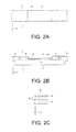
- FIG. 2A is a plan view of the antenna of FIG. 1 .
- FIG. 2B is a side view of the antenna of FIG. 1 .
- FIG. 2C is a cross-sectional view along Line C-C of the antenna of FIG. 1 .
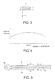
- FIG. 3 is a cross-sectional view of plate-shaped go-and-return conductors disposed in the up-down direction according to another embodiment of the present invention.
- FIG. 4 roughly illustrates the plasma density distributed along the longitudinal direction of a case in which a common and simple planar antenna is used.
- FIG. 5 is for illustrating the impedance of the two go-and-return conductors which are closely disposed to each other.
- FIG. 6 schematically shows a side view of an antenna in which the interval in the up-down direction of the two go-and-return conductors disposed in the up-down direction can be varied along the longitudinal direction of the antenna according to an embodiment of the present invention.
- FIG. 7 shows a model illustrating a simulation is performed in which the magnetic flux density near the central bottom of the antenna is varied and the interval in the up-down direction of the plate-shaped two go-and-return conductors disposed in the up-down direction is varied.
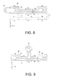
- FIG. 8 schematically shows a side view of an antenna in which the interval in the up-down direction of the two go-and-return conductors disposed in the up-down direction is varied along the longitudinal direction of the antenna according to another embodiment of the present invention.
- FIG. 9 schematically shows a side view of an antenna in which the interval in the up-down direction of the two go-and-return conductors disposed in the up-down direction is varied along the longitudinal direction of the antenna according to another embodiment of the present invention.
- FIG. 10 is a cross-sectional view of two rod-shaped go-and-return conductors disposed in the up-down direction according to an embodiment of the present invention.
- FIG. 11 is a cross-sectional view of two rod-shaped go-and-return conductors in which one conductor is plate-shaped and the other conductor is rod-shaped according to one embodiment of the present invention.
- FIG. 12 is a cross-sectional view of two rod-shaped go-and-return conductors in which one conductor is plate-shaped and the other conductor is rod-shaped according to another embodiment of the present invention.
- FIG. 13 shows a model illustrating a simulation is performed in which the magnetic flux density near the central bottom of the antenna is varied and the interval in the left-right direction of the plate-shaped two go-and-return conductors disposed in the left-right direction is varied.
- FIG. 14 shows a model illustrating a simulation is performed in which the magnetic flux density near the central bottom of the antenna is varied and the interval in the up-down direction of the rod-shaped two go-and-return conductors disposed in the up-down direction is varied.
- FIG. 15 shows a model illustrating a simulation is performed in which the magnetic flux density near the central bottom of the antenna is varied and the interval in the left-right direction of the rod-shaped two go-and-return conductors disposed in the left-right direction is varied.
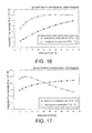
- FIG. 16 is a graph illustrating the variation of the magnetic flux density via the variation of the intervals respectively shown in the model of FIG. 7 (exemplary embodiment) and in the model of FIG. 13 (comparative example).
- FIG. 17 is a graph illustrating the variation of the magnetic flux density via the variation of the intervals respectively shown in the model of FIG. 14 (exemplary embodiment) and in the model of FIG. 15 (comparative example).
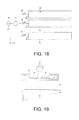
- FIG. 18 is a plan view showing that a plurality of antennas are disposed in parallel according to an embodiment of the present invention.
- FIG. 19 is a side view of a plasma processing apparatus according to another embodiment of the present invention.
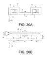
- FIG. 20A is a plan view of an antenna in which the interval in the left-right direction of the two go-and-return conductors disposed in the up-down direction is varied along the longitudinal direction of the antenna according to an embodiment of the present invention.
- FIG. 20B is a side view of an antenna in which the interval in the left-right direction of the two go-and-return conductors disposed in the up-down direction is varied along the longitudinal direction of the antenna according to an embodiment of the present invention.
- FIG. 1 A plasma processing apparatus according to an embodiment of the present invention is shown in FIG. 1 , and FIG. 2 shows the antenna of FIG. 1 .
- the Z direction is the direction of the perpendicular line 3 standing on a surface of the substrate 2.
- the Y direction is the direction intersecting (e.g., orthogonal to) the perpendicular line 3. These directions are respectively known as the up-down direction Z and the left-right direction Y to simplify the descriptions.
- the X direction is the direction intersecting (e.g., orthogonal to) the perpendicular line 3 and is the longitudinal direction of the antenna 30.
- the X direction and Y direction are horizontal, but it is not limited thereto.
- the foregoing descriptions of the X direction, Y direction and Z direction are applicable in other figures.
- the apparatus is an inductively-coupled plasma (ICP) type plasma processing apparatus.
- ICP inductively-coupled plasma
- a high frequency current I R from a high frequency power source 42 is applied to an antenna 30, that is substantially straight in a plan view of the antenna, in the apparatus so that an electric field is induced in a vacuum container 4 to generate a plasma 50, and the plasma 50 is used to perform a plasma treatment to a substrate 2.
- substantially straight not only represents “a straight status” according to the plan meaning of the words, but also represents “a nearly straight status”.
- the substrate 2 can be substrates used in flat panel displays (FPD) such as liquid crystal displays and organic electroluminescent displays, flexible substrates used in flexible displays, substrates used in solar cells of semiconductor display or the like; the present invention is not limited thereto.
- FPD flat panel displays
- the planar shape of the substrate 2 can be circular or quadrilateral, but the planar shape is not restricted in the present invention.
- the treatment process to the substrate 2 is forming a film by means of plasma CVD (chemical vapour deposition) process, etching, ashing, sputtering and the like.
- plasma CVD chemical vapour deposition
- the plasma processing apparatus is respectively called, a plasma CVD apparatus if it is used for the plasma CVD process, a plasma etching apparatus for etching process, a plasma ashing apparatus for ashing process, and a plasma sputtering apparatus for sputtering process.
- the plasma processing apparatus has a vacuum container 4 made of metal and the interior of the vacuum container 4 is vacuumed by using a vacuum exhaust device 8.
- a gas 24 is brought into the vacuum container 4 through an inlet pipe 22.
- the gas 24 may be any gas which is appropriate to the processing content of the substrate 2.
- the gas 24 is a source gas and a diluted source gas (e.g., H 2 ). More specifically, the source gas 24 is SiH 4 for a Si film, SiH 4 +NH 3 for a SiN film, SiH 4 +O 2 for a SiO 2 film formed on the substrate 2, respectively.
- a holder 10 is disposed in the vacuum container 4 to support the substrate 2.
- the holder 10 is supported by a shaft 16.
- the shaft 16 has a bearing portion 18 disposed at where the shaft 16 passes through the vacuum container 4, and the bearing portion 18 has the functions of electrical insulation and vacuum sealing.
- a bias power supply 20 can be provided for applying a negative bias voltage to the holder 10 via the shaft 16.
- the bias voltage can be a negative pulse voltage.
- the bias voltage not only can control the impinging energy generated when the positive ions of the plasma 50 impinge the substrate 2, but also can control the crystallinity of the film when the film is formed on the surface of the substrate 2.
- An antenna 30 is disposed at an opening 7 of the ceiling 6 of the vacuum container 4, and an insulating frame 38 is interposed between the antenna 30 and the opening 7. Packings 40 are respectively disposed for vacuum sealing between those components.
- the antenna 30 is disposed by using the two go-and-return conductors 31, 32 closely disposed to each other in the up-down direction Z.
- the antenna 30 (more particularly the two go-and-return conductors 31, 32 by which the antenna 30 is formed) has a surface with a planar shape. More specifically, the planar shape is a rectangular shape in this embodiment, but it is not limited thereto.
- the antenna 30 is described in detailed in the following.
- the material of the antenna 30 is copper (more particularly oxygen-free copper OFC), aluminum and the like, for example, but it is not restricted thereto.
- a high frequency power is applied to the antenna 30, more particularly to the go-and-return conductors 31 and 32, from a high frequency power source 42 through a matching circuit 44 so that a high frequency current I R flows to the antenna 30.
- the high frequency current (go-and-return current) I R flows in opposite directions between the two go-and-return conductors 31 and 32 by which the antenna 30 is formed (since it is a high frequency, the direction of the high frequency current I R reverses according to the time, and it is similar in the following).
- a high frequency magnetic field is generated due to the high frequency current I R , and a high frequency current I R and an electric field to the opposite direction are induced due to the high frequency magnetic field.
- the gas 24 near the antenna 30 is ionized and plasma 50 is formed near the antenna 30.
- the plasma 50 is diffused into the surrounding of the substrate 2, and the substrate 2 is treated by using the plasma 50.
- the frequency of the high frequency power output from the high frequency power source 42 is 13.56 MHz in general, but the present invention is not limited thereto.
- the total impedance Z T of the two go-and-return conductors 61 and 62 which are closely disposed in parallel, described in books, such as theory of electricity as a differential connection can be represented by the following equation.
- R 1 , L 1 are resistance and self-inductance of one of the conductors 61, respectively
- R 2 , L 2 are resistance and self-inductance of the other conductor 62, respectively
- M is mutual inductance of the two conductors 61 and 62.
- the total impedance Z T and the effective inductance L T are decreased as the mutual inductance M between the two go-and-return conductors 61 and 62 is increased.
- the electromagnetic energy G generated by using the flow of high frequency current I R from the high frequency power source 42 to the two go-and-return conductors 61 and 62 is represented in the following equation, wherein the electromagnetic energy G is decreased with an increase of the mutual inductance M, and the magnetic effect acting in the external is also decreased.
- the plasma density is decreased with a decrease of the electromagnetic energy provided to plasma, and vice versa.
- the mutual inductance M is not uniform along the longitudinal direction of the two go-and-return conductors 61 and 62, i.e., if the mutual inductance M is varied (in other words, if it is changed), for each region, the effective inductance and the electromagnetic energy are determined depending on the mutual inductance M of the region.
- the antenna 30 of the present invention is designed according to the foregoing mentioned principle.
- the antenna 30 is composed of the two go-and-return conductors 31 and 32 closely disposed to each other in the up-down direction Z.
- a two-stage change (a stepwise change) in the longitudinal direction X of the antenna 30 is designed, wherein the mutual inductance M 1 of the large interval D 1 of the region A 1 is greater than the mutual inductance M 2 of the small interval D 2 of the region A 2 (i.e., M 1 ⁇ M 2 ).
- the effective inductance of the region A 1 may be larger than the effective inductance of the region A 2 .
- Equation 4 regarding to the magnetic flux density of the space which is apart from the antenna 30 (more particularly the conductor 31) in a distance H 1 , the magnetic flux density B 1 of the region A 1 is greater than the magnetic flux density B 2 of the region A 2 (i.e., B 1 >B 2 ). Therefore, the plasma density of the region A 1 is capable of being greater than the plasma density of the region A 2 .
- the matching circuit 44 is disposed between the high frequency power source 42 and the antenna 30, as shown in FIG. 1 .
- the thickness T of the two conductors is 3 mm
- the width W of the left-right direction Y is 70 mm
- the X direction is defined to be sufficiently long
- the magnetic flux density B within a space which is apart from the point P in the distance H 1 (fixed at 5 mm) located at the central bottom in the left-right direction Y of the conductor 31 and the interval D is varied when a certain high frequency current I R (peak value is 100 A) is applied.
- the magnetic flux density B 0 of Table 1 is the magnetic flux density at the point P of a common antenna just having the conductor 31 and without the conductor 32.
- Such magnetic flux density B 0 , the ratio of magnetic flux density B/B 0 in the case of two go-and-return conductors 31 and 32 and the square of the ratio thereof ((B/B 0 ) 2 ) are described in Table 1. It can be noted that regarding the square of the magnetic flux density ratio (B/B 0 ) 2 , the eddy current loss is approximately proportional to the square of the magnetic flux density B when the electromagnetic energy is supplied for the plasma.
- the interval D is in the up-down direction Z of the two go-and-return conductors 31 and 32 closely disposed to each other in the up-down direction Z.
- the electromagnetic energy supplied for the plasma from the antenna 30 in the regions A 1 and A 3 can be relatively increased to be greater than the electromagnetic energy in the region A 2 .
- the antenna 30 illustrated in FIG. 1 and FIG. 2A to 2C is similar to the antenna 30 illustrated in FIG. 8 , a more specifically illustrated embodiment.
- the antenna 30 includes two go-and-return conductors 31 and 32 closely disposed to each other with an interval D in the up-down direction Z.
- the two conductors 31 and 32 are a plate shape, and are rectangular as mentioned above.
- the underside of the conductor 31 at the lower side (side of plasma 50) is located in a vacuum within the vacuum container 4 and the conductor 32 at the upper side is located in an ambient atmosphere.
- One of the terminals of the conductor 31 and one of the terminals of the conductor 32 are electrically opened, and an insulating material 36 is disposed therebetween in this embodiment.
- the other terminal of the conductor 31 and the other terminal of the conductor 32 are electrically connected at a connecting portion 33.
- the high frequency power is supplied to the interval between the terminals of conductors 31 and 32 from the high frequency power source 42 through the matching circuit 44.
- the two conductors 31 and 32 are a plate shape in this embodiment (more particularly the conductor 31 is a plate shape, and the conductor 32 is a bended plate shape).
- the conductor 31 at the lower side can be designed to have a larger thickness as shown in FIG. 1 and FIG. 2C
- the two conductors 31 and 32 can be designed to have the same thickness as shown in FIG. 3 .
- the interval D and the mutual inductance M of the antenna 30 can be varied in a stepwise manner along the longitudinal direction X of the antenna 30 as shown in FIG. 1 and FIG. 8 , or they can also be varied continuously.
- the manner of variation of the interval D and the mutual inductance M of the antenna 30 is similar in the following embodiments. Even if the interval D is varied in a stepwise manner, since the plasma has a diffusion effect, the plasma density can be smoothly varied.
- the interval D and the mutual inductance M of the antenna 30 can be continuously varied in the longitudinal direction X of the antenna 30 by disposing a gently-sloping valley recessed at the central portion of the conductor 32 of FIG. 1 and FIG. 2A to 2C at the upper side.
- the antenna 30 can also be designed in manner similar to that of the antenna 30 as shown in FIG. 6 . Moreover, the antenna 30 can also be designed in a manner the same as that of the antenna 30 shown in FIG. 9 .
- FIG. 9 illustrates a different antenna 30 from FIG. 1 and FIG. 8 .
- the high frequency power can be supplied from the central portion (center power supply) of the antenna.
- the center power supply can be applied in the antenna 30 in other embodiments.
- the go-and-return conductors 31 and 32 which form the antenna 30 can be a plate shape as described in the aforementioned embodiments, a rod shape as shown in FIG. 10 and a combination of rod and plate shape.
- the conductor 31 at the lower side is a plate shape and the conductor 32 at the upper side is a rod shape.
- the conductors 32 at the upper side can also be electrically disposed in parallel (two conductors 32 are shown in FIG. 12 ).
- the go-and-return conductors 31 and 32 are electrically connected to each other at the connecting portion (please refer to the connecting portion 33 of FIG. 1 ) in the longitudinal direction X.
- each conductor 31 and 32 is not limited in the present invention, and they can be circular, elliptical, tetragonal or the like.
- each of the conductors 31 and 32 can be hollowed so that a coolant or cooling water can flow there-through for cooling the conductors 31 and 32.
- the antenna 30 is composed of two go-and-return conductors 31 and 32 closely disposed to each other in the up-down direction Z in which a high frequency current I R flows in opposite directions.
- the effective inductance decreases due to the mutual inductance between the go-and-return conductors 31 and 32. Since almost the whole impedance of the antenna 30 is inductance in the high frequency region, the potential difference generated in the antenna 30 can be suppressed to be small because of the decrease of the effective inductance. Thus, the potential of the antenna 30 can be suppressed to be small and the potential of the plasma 50 can also be suppressed to be small.
- the energy of the charged particles (e.g., ions) impinging to the substrate 2 from the plasma 50 can be suppressed to be small. Accordingly, for example, when a film is formed on the substrate 2 by using the plasma 50, the damage formed on the film can be suppressed to the minimum and the film quality can also be improved. Moreover, even if the antenna 30 is increased in length, according to the above mentioned reason, since the potential of the antenna 30 can be suppressed to be small and the potential of the plasma 50 can also be suppressed to be small, it is easy to correspondingly increase the size of the substrate 2 with the increased length of the antenna 30.
- the potential of the antenna 30 can be suppressed to be small and the potential of the plasma 50 can also be suppressed to be small, it is easy to correspondingly increase the size of the substrate 2 with the increased length of the antenna 30.
- the mutual inductance M between the go-and-return conductors 31 and 32 can be varied along the longitudinal direction X of the antenna 30 according to the interval D of the go-and-return conductors in the up-down direction Z being changed along the longitudinal direction X of the antenna 30, the electromagnetic energy supplied for the plasma 50 from the antenna 30 can be varied along the longitudinal direction X of the antenna 30. Accordingly, the plasma density distributed along the longitudinal direction X of the antenna 30 can be controlled. As a result, the processing status of the substrate 2 in the longitudinal direction X of the antenna 30 can be controlled. For example, when a film is formed on the substrate 2 by using the plasma 50, the film thickness distributed along the longitudinal direction X of the antenna 30 can be controlled.
- the antenna 30 is composed of two go-and-return conductors 31 and 32 closely disposed to each other in the up-down direction Z in which a high frequency current I R flows in opposite directions and the interval D in the up-down direction Z of the go-and-return conductors 31 and 32 can be varied along the longitudinal direction X of the antenna 30, compared to the condition of the interval in the left-right direction Y between the go-and-return conductors closely disposed to each other in the left-right direction being capable to be varied, the magnetic flux density near the bottom of the antenna 30 can be well controlled according to the variation of the interval D of the go-and-return conductors 31 and 32. Accordingly, the electromagnetic energy supplied for the plasma 50 from the antenna 30 can be well controlled because of the interval D of the go-and-return conductors 31 and 32 can be varied. Consequently, the plasma density distribution can be well controlled, and the simulation result is described as follow.
- the variation of the magnetic flux density B, at the point P (referring to FIG. 7 , FIG. 13 to FIG. 15 ) located at the central region below, in the left-right direction Y of the antenna 30 is calculated, when the interval D of the go-and-return conductors 31 and 32 of the antenna 30 is varied.
- the calculated variation values of the magnetic flux density B at the point P when the interval D in the up-down direction Z between the go-and-return conductors 31 and 32 is varied are shown in FIG. 16 .
- the calculation condition is the same as that described in FIG. 7 , and thus the magnetic flux density B is the same as that in Table 1.
- the calculated variation values of the magnetic flux density B at the point P when the interval D in the left-right direction Y between the go-and-return conductors 31 and 32 is varied are shown in FIG. 16 .
- the calculation condition is as follow : the thickness T of the two conductors 31 and 32 is 70mm, the width W in the left-right direction Y is 3 mm, and the values of the distance H 1 , the high frequency current I R and so on are the same as those described in FIG. 7 .
- the variation of the magnetic flux density B becomes saturated very soon (i.e., the magnetic flux density B does not varies so much with the variation of the interval D).
- the magnetic flux density B is proportionally and mildly varied and the variation range is large. Accordingly, compared to the comparative example, the control of the magnetic flux density B in the exemplary embodiment is better. Namely, according to the variation of the interval D, the electromagnetic energy supplied for the plasma 50 from the antenna 30 can be controlled by controlling the magnetic flux density B, and consequently the control of the plasma density distribution can become easier.
- the variation values of the magnetic flux density B at the point P calculated when the interval D in the up-down direction Z between the go-and-return conductors 31 and 32 is varied are shown in FIG. 17 .
- the calculation condition is as follow: the diameter d of the two conductors 31 and 32 is 6 mm, and the values of the distance H 1 , the high frequency current I R and so on are the same as those described in FIG. 7 .
- the variation of the magnetic flux density B is complex as the variation goes up and down subsequently.
- the magnetic flux density B is proportionally and mildly varied. Accordingly, compared to the comparative example, the control of the magnetic flux density B in the exemplary embodiment is better. Namely, according to the variation of the interval D, the electromagnetic energy supplied for the plasma 50 from the antenna 30 can be controlled by controlling the magnetic flux density B, and consequently the control of the plasma density distribution can become easier.
- the go-and-return conductors 31 and 32 of the antenna 30 can be closely disposed to each other in the up-down direction Z, and the mutual inductance between the go-and-return conductors 31 and 32 can be varied along the longitudinal direction X of the antenna 30 as the interval D located in the left-right direction Y and between the go-and-return conductors 31 and 32 is varied along the longitudinal direction X of the antenna 30.
- the electromagnetic energy supplied for the plasma 50 from the antenna 30 at the regions A 1 and A 3 of the two terminals can be relatively increased to be greater than the electromagnetic energy in the central portion of the region A 2 .
- the plasma density distribution thereof in the longitudinal direction is shown as FIG. 4 , the plasma density distributed at the two terminals is smaller than the plasma density distributed at the central portion, i.e., a mountain-shaped distribution. It can be simply explained that the plasma is diffused from two sides at the central portion whereas the plasma is diffused from single side at each of the two terminals.
- the mutual inductance in the longitudinal direction X of the antenna 30 at the two terminals can be reduced to be smaller than the mutual inductance at the central portion by means of increasing the interval D between the go-and-return conductors 31 and 32 located in the up-down direction Z in the longitudinal direction X of the antenna 30 at the two terminals to be larger than the interval at the central portion. Therefore, the effective inductance at the two terminals of the antenna 30 is relatively greater than that at the central portion. As a result, contrary to the mountain-shaped, the electromagnetic energy supplied for plasma 50 from the antenna 30 in the longitudinal direction X of the antenna 30 at the two terminals is relatively greater than the electromagnetic energy at the central portion.
- the plasma 50 is more strongly generated at the two terminals than it is generated at the central portion. Accordingly, the mountain-shaped plasma density distribution is compensated, and the plasma density distribution can be homogeneously enhanced in the longitudinal direction X of the antenna 30. For example, when a film is formed on the substrate 2 by using the plasma 50, homogeneity of the film thickness in the longitudinal direction X of the antenna 30 can be improved.
- a shielding plate 46 for shielding the inner side surface of the vacuum container 4 against the plasma 50 can also be disposed in the plasma processing apparatus.
- the shielding plate 46 is made with an insulating material.
- the shielding plate 46 can be directly mounted near the inlet of the opening 7 of the ceiling 6 of the vacuum container 4, and it can also be mounted by using a frame-shaped supporting plate 48 as shown in this embodiment.
- the shielding plate 46 can also be used in the antenna 30 of other embodiments.
- the material of the shielding plate 46 can be quartz, aluminum, silicon carbide, silicon and the like. In order to avoid the problem of releasing oxygen out of the shielding plate 46 due to the deoxidization in hydrogen-based plasma, it is preferred to use the non-oxide materials such as silicon, silicon carbide and the like. For example, it is simple to use a silicon plate.
- the shielding plate 46 Through the disposition of the shielding plate 46, adverse conditions, such as metal contamination of the surface of the substrate 2 and the plasma 50 due to the charged particles (mainly ions) of the plasma 50 sputtering on the antenna 30 surface can be prevented.
- the shielding plate 46 Even if the shielding plate 46 is disposed, the shielding plate 46 cannot prevent the potential of the antenna 30 to reach the plasma 50 because the shielding plate is made of an insulating material. Therefore, the potential of the antenna 30 can be suppressed effectively by reducing the effective inductance of the antenna 30 as in the above mentioned manner.
- a plurality of antennas 30 can be disposed in parallel in the Y direction, and the high frequency power can be supplied simultaneously to the antennas 30 from a common high frequency power source 42 through the variable impedances 52 respectively connected to the antennas 30 in series.
- Each of the antennas 30 can be designed as one of the antennas shown in FIG. 1 , FIG. 2A to 2C , FIG. 6 , FIG. 8 and FIG. 9 .
- the variable impedance 52 can be the variable inductance shown in FIG. 18 , the variable condenser (variable capacitance), or a combination thereof. Since the impedance of the feed circuit can be increased by inserting the variable inductance, the current of the antenna 30, at which the high frequency current becomes overflown, can be suppressed. The impedance of the feed circuit can be decreased and the capacitive reactance can be increased when the inductive reactance is large by inserting the variable condenser. Accordingly, the current of the antenna 30, at which the high frequency current becomes difficult to flow, can also be increased.
- the to be treated substrate 2 is immovably fixed in the vacuum container 4.
- the substrate 2 can also be disposed in the vacuum container 4 (omitted in FIG. 19 ), in which the substrate 2 can be moved in a direction as shown with an arrow F (and its opposite direction) intersecting (e.g., orthogonal) with the longitudinal direction X of the antenna 30 by using a substrate carrying device 54, i.e., the substrate 2 can be processed as it is moving along the Y direction. Accordingly, the homogeneity of the plasma 50 in the X direction can be enhanced due to the antenna 30.
- the antenna 30 can be one of the antennas shown in FIG. 1 , FIG. 2A to 2C , FIG. 6 , FIG. 8 and FIG. 9 .
- the idea of the substrate 2 being carried can also be used and combined with the idea of having a plurality of antennas 30 disposed in parallel shown in FIG. 18 .
Landscapes
- Engineering & Computer Science (AREA)
- Chemical & Material Sciences (AREA)
- Physics & Mathematics (AREA)
- Plasma & Fusion (AREA)
- Analytical Chemistry (AREA)
- General Chemical & Material Sciences (AREA)
- Materials Engineering (AREA)
- Mechanical Engineering (AREA)
- Metallurgy (AREA)
- Organic Chemistry (AREA)
- Electromagnetism (AREA)
- Spectroscopy & Molecular Physics (AREA)
- Chemical Kinetics & Catalysis (AREA)
- Plasma Technology (AREA)
- Chemical Vapour Deposition (AREA)
- Drying Of Semiconductors (AREA)
Applications Claiming Priority (1)
| Application Number | Priority Date | Filing Date | Title |
|---|---|---|---|
| JP2011140128A JP4844697B1 (ja) | 2011-06-24 | 2011-06-24 | プラズマ処理装置 |
Publications (1)
| Publication Number | Publication Date |
|---|---|
| EP2538432A2 true EP2538432A2 (fr) | 2012-12-26 |
Family
ID=45475262
Family Applications (1)
| Application Number | Title | Priority Date | Filing Date |
|---|---|---|---|
| EP12165316A Withdrawn EP2538432A2 (fr) | 2011-06-24 | 2012-04-24 | Appareil de traitement par plasma |
Country Status (6)
| Country | Link |
|---|---|
| US (1) | US8372239B2 (fr) |
| EP (1) | EP2538432A2 (fr) |
| JP (1) | JP4844697B1 (fr) |
| KR (1) | KR101245844B1 (fr) |
| CN (1) | CN102647847B (fr) |
| TW (1) | TWI382791B (fr) |
Cited By (2)
| Publication number | Priority date | Publication date | Assignee | Title |
|---|---|---|---|---|
| EP3629362A1 (fr) * | 2018-09-25 | 2020-04-01 | Plasma Ion Assist Co. Ltd. | Appareil de traitement par plasma et son procédé de commande |
| US12327709B2 (en) | 2016-10-24 | 2025-06-10 | Samsung Electronics Co., Ltd. | Antennas, circuits for generating plasma, plasma processing apparatus, and methods of manufacturing semiconductor devices using the same |
Families Citing this family (9)
| Publication number | Priority date | Publication date | Assignee | Title |
|---|---|---|---|---|
| JP2013134835A (ja) * | 2011-12-26 | 2013-07-08 | Nissin Electric Co Ltd | プラズマ処理装置 |
| DE112014000730T5 (de) * | 2013-02-08 | 2015-10-15 | Norma U.S. Holding Llc | Kraftstoffleitung-Verbindungsanordung |
| KR101582838B1 (ko) * | 2013-08-23 | 2016-01-12 | 니신 일렉트릭 컴패니 리미티드 | 플라즈마 처리장치 |
| US20180096823A1 (en) * | 2016-09-30 | 2018-04-05 | Intevac, Inc. | Large area energetic ion source |
| KR102630343B1 (ko) * | 2017-08-03 | 2024-01-30 | 삼성전자주식회사 | 플라즈마 처리 장치 및 그를 이용한 반도체 소자의 제조방법 |
| KR102782333B1 (ko) * | 2016-10-24 | 2025-03-19 | 삼성전자주식회사 | 안테나, 플라즈마 생성 회로, 플라즈마 처리 장치, 및 그를 이용한 반도체 소자의 제조방법 |
| CN115537917A (zh) * | 2022-10-10 | 2022-12-30 | 浙江合特光电有限公司 | 一种钙钛矿外延生长工艺及用于该工艺的沉积设备 |
| US12463011B2 (en) | 2023-11-11 | 2025-11-04 | Applied Materials Inc. | Inductively coupled plasma source with radial coil network |
| US20250349509A1 (en) * | 2024-05-13 | 2025-11-13 | Applied Materials, Inc. | Methods and apparatus that use inductively coupled plasma resonator sources |
Citations (1)
| Publication number | Priority date | Publication date | Assignee | Title |
|---|---|---|---|---|
| WO2009142016A1 (fr) | 2008-05-22 | 2009-11-26 | 株式会社イー・エム・ディー | Appareil de génération de plasma et appareil de traitement par plasma |
Family Cites Families (12)
| Publication number | Priority date | Publication date | Assignee | Title |
|---|---|---|---|---|
| JP3117366B2 (ja) * | 1994-07-25 | 2000-12-11 | 三菱重工業株式会社 | プラズマ処理装置 |
| JPH11317299A (ja) * | 1998-02-17 | 1999-11-16 | Toshiba Corp | 高周波放電方法及びその装置並びに高周波処理装置 |
| JP5017762B2 (ja) | 2001-09-27 | 2012-09-05 | 株式会社Ihi | 放電装置、プラズマ処理方法 |
| JP2006216903A (ja) * | 2005-02-07 | 2006-08-17 | Hitachi High-Technologies Corp | プラズマ処理装置 |
| KR100689848B1 (ko) * | 2005-07-22 | 2007-03-08 | 삼성전자주식회사 | 기판처리장치 |
| JP4707588B2 (ja) * | 2006-03-16 | 2011-06-22 | 東京エレクトロン株式会社 | プラズマ処理装置及びそれに用いられる電極 |
| US20080110567A1 (en) * | 2006-11-15 | 2008-05-15 | Miller Matthew L | Plasma confinement baffle and flow equalizer for enhanced magnetic control of plasma radial distribution |
| JP5479867B2 (ja) * | 2009-01-14 | 2014-04-23 | 東京エレクトロン株式会社 | 誘導結合プラズマ処理装置 |
| JP2010225296A (ja) * | 2009-03-19 | 2010-10-07 | Emd:Kk | 誘導結合型アンテナユニット及びプラズマ処理装置 |
| JP5231308B2 (ja) * | 2009-03-31 | 2013-07-10 | 東京エレクトロン株式会社 | プラズマ処理装置 |
| JP5592098B2 (ja) * | 2009-10-27 | 2014-09-17 | 東京エレクトロン株式会社 | プラズマ処理装置及びプラズマ処理方法 |
| JP5554047B2 (ja) * | 2009-10-27 | 2014-07-23 | 東京エレクトロン株式会社 | プラズマ処理装置 |
-
2011
- 2011-06-24 JP JP2011140128A patent/JP4844697B1/ja active Active
-
2012
- 2012-04-17 US US13/449,304 patent/US8372239B2/en not_active Expired - Fee Related
- 2012-04-24 EP EP12165316A patent/EP2538432A2/fr not_active Withdrawn
- 2012-04-25 KR KR1020120043054A patent/KR101245844B1/ko not_active Expired - Fee Related
- 2012-04-26 CN CN2012101276274A patent/CN102647847B/zh not_active Expired - Fee Related
- 2012-05-15 TW TW101117239A patent/TWI382791B/zh not_active IP Right Cessation
Patent Citations (1)
| Publication number | Priority date | Publication date | Assignee | Title |
|---|---|---|---|---|
| WO2009142016A1 (fr) | 2008-05-22 | 2009-11-26 | 株式会社イー・エム・ディー | Appareil de génération de plasma et appareil de traitement par plasma |
Cited By (3)
| Publication number | Priority date | Publication date | Assignee | Title |
|---|---|---|---|---|
| US12327709B2 (en) | 2016-10-24 | 2025-06-10 | Samsung Electronics Co., Ltd. | Antennas, circuits for generating plasma, plasma processing apparatus, and methods of manufacturing semiconductor devices using the same |
| EP3629362A1 (fr) * | 2018-09-25 | 2020-04-01 | Plasma Ion Assist Co. Ltd. | Appareil de traitement par plasma et son procédé de commande |
| US11164728B2 (en) | 2018-09-25 | 2021-11-02 | Plasma Ion Assist Co., Ltd. | Plasma treatment apparatus and driving method thereof |
Also Published As
| Publication number | Publication date |
|---|---|
| TW201244550A (en) | 2012-11-01 |
| US20120325404A1 (en) | 2012-12-27 |
| KR20130007413A (ko) | 2013-01-18 |
| TWI382791B (zh) | 2013-01-11 |
| CN102647847B (zh) | 2013-07-10 |
| CN102647847A (zh) | 2012-08-22 |
| KR101245844B1 (ko) | 2013-03-22 |
| JP2013008539A (ja) | 2013-01-10 |
| JP4844697B1 (ja) | 2011-12-28 |
| US8372239B2 (en) | 2013-02-12 |
Similar Documents
| Publication | Publication Date | Title |
|---|---|---|
| US8372239B2 (en) | Plasma processing apparatus | |
| KR101591404B1 (ko) | 플라즈마 생성장치 및 플라즈마 처리장치 | |
| US12255052B2 (en) | Process control for ion energy delivery using multiple generators and phase control | |
| US9583313B2 (en) | Plasma processing apparatus and plasma processing method | |
| WO2020022141A1 (fr) | Dispositif de traitement au plasma | |
| US7098599B2 (en) | Plasma generator | |
| TW200845200A (en) | Methods to eliminate "M-shape" etch rate profile in inductively coupled plasma reactor | |
| US20230298866A1 (en) | Plasma uniformity control using a static magnetic field | |
| JP2017033788A (ja) | プラズマ処理装置 | |
| TWI770144B (zh) | 電漿處理裝置 | |
| KR101167952B1 (ko) | 대면적의 플라즈마를 발생시키는 플라즈마 반응기 | |
| KR101585893B1 (ko) | 복합형 플라즈마 반응기 | |
| US8394232B1 (en) | Plasma processing apparatus | |
| TW202102066A (zh) | 接地帶組件 | |
| JP2013020871A (ja) | プラズマ処理装置 | |
| CN101855707B (zh) | 等离子处理装置 | |
| JP2013134836A (ja) | プラズマ処理装置 | |
| WO2013099366A1 (fr) | Dispositif de traitement plasma | |
| KR101585891B1 (ko) | 혼합형 플라즈마 반응기 | |
| JP2016072065A (ja) | プラズマ処理装置 | |
| JP2013131295A (ja) | プラズマ処理装置 | |
| WO2012176242A1 (fr) | Dispositif de traitement par plasma | |
| KR101798376B1 (ko) | 유도결합 플라즈마 처리장치의 유전체창 | |
| JP2006080192A (ja) | プラズマプロセス装置 | |
| KR20260016460A (ko) | 대면적 기판들을 위한 침지 플라즈마 소스 및 프로세스 챔버 |
Legal Events
| Date | Code | Title | Description |
|---|---|---|---|
| PUAI | Public reference made under article 153(3) epc to a published international application that has entered the european phase |
Free format text: ORIGINAL CODE: 0009012 |
|
| 17P | Request for examination filed |
Effective date: 20120424 |
|
| AK | Designated contracting states |
Kind code of ref document: A2 Designated state(s): AL AT BE BG CH CY CZ DE DK EE ES FI FR GB GR HR HU IE IS IT LI LT LU LV MC MK MT NL NO PL PT RO RS SE SI SK SM TR |
|
| AX | Request for extension of the european patent |
Extension state: BA ME |
|
| STAA | Information on the status of an ep patent application or granted ep patent |
Free format text: STATUS: THE APPLICATION HAS BEEN WITHDRAWN |
|
| 18W | Application withdrawn |
Effective date: 20130318 |