EP2541404B1 - Technique pour l'exécution de séquence de tâche - Google Patents
Technique pour l'exécution de séquence de tâche Download PDFInfo
- Publication number
- EP2541404B1 EP2541404B1 EP11005362.6A EP11005362A EP2541404B1 EP 2541404 B1 EP2541404 B1 EP 2541404B1 EP 11005362 A EP11005362 A EP 11005362A EP 2541404 B1 EP2541404 B1 EP 2541404B1
- Authority
- EP
- European Patent Office
- Prior art keywords
- load module
- chip memory
- load
- chip
- memory
- Prior art date
- Legal status (The legal status is an assumption and is not a legal conclusion. Google has not performed a legal analysis and makes no representation as to the accuracy of the status listed.)
- Not-in-force
Links
Images



Classifications
-
- G—PHYSICS
- G06—COMPUTING OR CALCULATING; COUNTING
- G06F—ELECTRIC DIGITAL DATA PROCESSING
- G06F9/00—Arrangements for program control, e.g. control units
- G06F9/06—Arrangements for program control, e.g. control units using stored programs, i.e. using an internal store of processing equipment to receive or retain programs
- G06F9/46—Multiprogramming arrangements
- G06F9/48—Program initiating; Program switching, e.g. by interrupt
-
- G—PHYSICS
- G06—COMPUTING OR CALCULATING; COUNTING
- G06F—ELECTRIC DIGITAL DATA PROCESSING
- G06F9/00—Arrangements for program control, e.g. control units
- G06F9/06—Arrangements for program control, e.g. control units using stored programs, i.e. using an internal store of processing equipment to receive or retain programs
- G06F9/46—Multiprogramming arrangements
- G06F9/48—Program initiating; Program switching, e.g. by interrupt
- G06F9/4806—Task transfer initiation or dispatching
- G06F9/4843—Task transfer initiation or dispatching by program, e.g. task dispatcher, supervisor, operating system
- G06F9/4881—Scheduling strategies for dispatcher, e.g. round robin, multi-level priority queues
-
- G—PHYSICS
- G06—COMPUTING OR CALCULATING; COUNTING
- G06F—ELECTRIC DIGITAL DATA PROCESSING
- G06F12/00—Accessing, addressing or allocating within memory systems or architectures
- G06F12/02—Addressing or allocation; Relocation
- G06F12/08—Addressing or allocation; Relocation in hierarchically structured memory systems, e.g. virtual memory systems
-
- G—PHYSICS
- G06—COMPUTING OR CALCULATING; COUNTING
- G06F—ELECTRIC DIGITAL DATA PROCESSING
- G06F2212/00—Indexing scheme relating to accessing, addressing or allocation within memory systems or architectures
- G06F2212/25—Using a specific main memory architecture
- G06F2212/251—Local memory within processor subsystem
-
- G—PHYSICS
- G06—COMPUTING OR CALCULATING; COUNTING
- G06F—ELECTRIC DIGITAL DATA PROCESSING
- G06F2212/00—Indexing scheme relating to accessing, addressing or allocation within memory systems or architectures
- G06F2212/25—Using a specific main memory architecture
- G06F2212/253—Centralized memory
-
- Y—GENERAL TAGGING OF NEW TECHNOLOGICAL DEVELOPMENTS; GENERAL TAGGING OF CROSS-SECTIONAL TECHNOLOGIES SPANNING OVER SEVERAL SECTIONS OF THE IPC; TECHNICAL SUBJECTS COVERED BY FORMER USPC CROSS-REFERENCE ART COLLECTIONS [XRACs] AND DIGESTS
- Y02—TECHNOLOGIES OR APPLICATIONS FOR MITIGATION OR ADAPTATION AGAINST CLIMATE CHANGE
- Y02D—CLIMATE CHANGE MITIGATION TECHNOLOGIES IN INFORMATION AND COMMUNICATION TECHNOLOGIES [ICT], I.E. INFORMATION AND COMMUNICATION TECHNOLOGIES AIMING AT THE REDUCTION OF THEIR OWN ENERGY USE
- Y02D10/00—Energy efficient computing, e.g. low power processors, power management or thermal management
Definitions
- the present disclosure generally relates to the technical field of computing systems.
- the present disclosure relates to a technique of executing a task sequence on a computing system comprising a multiple task processor having an on-chip memory and further comprising an external memory connected to the multiple task processor.
- DSP Digital Signal Processor
- the multiple task processor is used as an accelerator to speed up algorithms that require regular processing.
- a set of instructions for the multiple task processor is called a program which, alone or together with other programs, carries out a task (e.g., a function) when executed on the multiple task processor.
- the program is stored in a program memory. The execution of the program may require constant data and variable data which are typically stored in an optional data memory.
- the program memory and the data memory are often realized as on-chip program memory and an on-chip data memory (in the following also summarized as "on-chip memory") of the multiple task processor since executing programs from an external memory increases the execution time of the programs.
- on-chip memory allows the core of the multiple task processor to have high speed access, the size of the on-chip memory is typically limited. Thus, if several tasks have to be carried out by the multiple task processor, it is often the case that the size of the on-chip memory is not large enough to store the programs (and the data) for all tasks at the same time.
- programs and data for all tasks may initially be stored in an external memory which is slow in access but large in size.
- the programs and data corresponding to the task to be executed are transferred from the external memory into the on-chip memory of the multiple task processor, typically using Direct Memory Access (DMA).
- DMA Direct Memory Access
- a control processor in the embedded system may control this transfer process (e.g., ensure that the programs and data needed to execute a task have been properly loaded into the on-chip memory of the multiple task processor before the multiple task processor is asked to execute the task).
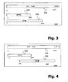
- Fig. 3 shows schematically how programs and data needed to execute tasks are stored within an on-chip memory 300 in existing computing systems which comprise a multiple task processor having an on-chip memory and which further comprise an external memory connected to the multiple task processor.
- the on-chip memory 300 has an exemplary memory capacity of 120KB as indicated by reference numeral 310.
- programs and data needed to execute task A are referred to as load module A.
- Programs and data needed to execute task B are referred to as load module B.
- the memory size of load module A is 60KB, and its location within the on-chip memory 300 is indicated by reference numeral 320, whereas the memory size of load module B is 90KB, and its location within the on-chip memory 300 is indicated by reference numeral 330.
- load module A is overlaid with load module B.
- each load module is copied such into the on-chip memory 300 that the memory start address of each load module respectively coincides with the memory start address of the on-chip memory 300 (here: start address 0).
- load module A is completely overwritten by load module B when load module B is copied into the on-chip memory 300 after having copied load module A into the on-chip memory 300
- load module B is partly overwritten by load module A when load module A is copied into the on-chip memory 300 after having copied load module B into the on-chip memory 300.
- Document US 2005/066132 A1 discloses a processor having an on-chip memory which is managed by a cache controller, and an external memory. Instructions retrieved from the external memory are cached in the on-chip memory before they are executed by the processor.
- Document WO 2009/120479 A2 discloses a tightly coupled memory system, in particular a processor having an on-chip memory which is managed by a cache controller, and an external memory. Instructions retrieved from the external memory are cached in the on-chip memory before they are executed by the processor.
- a method for executing a task sequence on a system comprising a multiple task processor having an on-chip memory and an external memory connected to the multiple task processor.
- the method comprises transferring load module data from the external memory into the on-chip memory in order to generate a load module sequence within the on-chip memory, wherein a load module includes at least one of a program and data to be processed by the program.
- the generation of a load module of the load module sequence comprises the following processes: determining, based on respective start addresses and end addresses of the load modules of the load module sequence, based on a respective first indicator indicating whether the load module has already been completely loaded at least once into the on-chip memory, and based on a respective second indicator indicating whether at least a part of the load module, after having been completely loaded into the on-chip memory, is currently overwritten, which parts of the load module are currently stored within the on-chip memory, and transferring only load module data from the external memory into the on-chip memory for parts of the load module which are currently not stored within the on-chip memory.
- the load module is completely loaded into the on-chip memory if the first indicator is in a FALSE state, the load module is partly loaded into the on-chip memory if the first indicator is in a TRUE state and the second indicator is in a FALSE state, and no part of the load module is loaded into the on-chip memory if the first indicator and the second indicator are respectively in a TRUE state, wherein each load module of the load module sequence is generated within an individual address range of the on-chip memory which is chosen in dependence on the load module sequence.
- the method further comprises executing the task sequence by running the load module sequence.
- choosing an individual address range of the on-chip memory in dependence on the load module sequence may comprise choosing an individual address range in dependence on a parameter or a set of parameters which characterizes the load module sequence.
- load module sequence characterizing parameters may for example include at least one of the size and the order of the load modules, but the technique presented herein is not restricted to these parameters.
- a load module sequence characterizing parameter may also include the number of load module downloading cycles of a repeating pattern of the load module sequence, or the like.
- the address ranges of the load modules of the load module sequence may be chosen in various ways.
- the load modules may be chosen such that the amount of load module data transferred from the external memory into the on-chip memory is reduced (e.g., minimized).
- At least one of start addresses and end addresses of the address ranges of the load modules may be chosen depending on one or both of the size of the load modules and the order according to which the load modules are generated within the on-chip memory. In this way, very short (average) load module download times can be obtained. Additionally, or as an alternative, at least one of start addresses and end addresses of the load modules within the on-chip memory may be chosen such that as much address range of the on-chip memory as possible is covered by the load modules.
- At least one of start addresses and end addresses of the load modules within the on-chip memory may be chosen such that, in case that the sum of the data lengths of the load modules already generated within the on-chip memory is smaller than the total data size of the on-chip memory, the address ranges of load module data of different load modules do not overlap with each other. Moreover, in case that the sum of the data lengths of the load modules already generated within the on-chip memory is larger than the total data size of the on-chip memory, the whole address range of the on-chip memory may be covered by load module data of the load modules. In this way, it may in certain implementations be ensured that as much address range as possible is covered by the load modules (thus shortening the download times).
- Load modules may be successively generated within the on-chip memory.
- a start address assigned to a load module currently generated within the on-chip memory may be located immediately after the end address of a load module previously generated.
- an end address may be assigned to the further load module which coincides with the highest address of the on-chip memory.
- a start address assigned to a first load module generated within the on-chip memory may coincide with the lowest address of the on-chip memory.
- Determining which parts of the load module are currently stored within the on-chip memory and/or which module data is to be downloaded may be at least partly controlled by the multiple task processor.
- the multiple task processor may be a Digital Signal Processor.
- a computer program product comprising program code portions for performing any one of the above described embodiments when the computer program product is executed on a computing device.
- the computing device may comprise at least one of the multiple task processor and a dedicated control processor.
- a computer-readable recording medium storing the computer program product is provided.
- the computer-readable recording medium may take the form of a semiconductor memory, a CD-ROM or DVD.
- the computer program product may be provided for download onto such a computer-readable medium (e.g., via a network connection).
- a computing system comprising a multiple task processor having an on-chip memory and further comprising an external memory connected to the multiple task processor.
- the computing system is adapted to transfer load module data from the external memory into the on-chip memory in order to generate a load module sequence within the on-chip memory, wherein a load module includes at least one of a program and data to be processed by the program.
- the generation of a load module of the load module sequence comprises the following processes: determining, based on respective start addresses and end addresses of the load modules of the load module sequence, based on a respective first indicators indicating whether the load module has already been completely loaded at least once into the on-chip memory, and based on a respective second indicator indicating whether at least a part of the load module, after having been completely loaded into the on-chip memory, is currently overwritten, which parts of the load module are currently stored within the on-chip memory, and transferring only load module data from the external memory into the on-chip memory for parts of the load module which are currently not stored within the on-chip memory.
- the load module is completely loaded into the on-chip memory if the first indicator is in a FALSE state, the load module is partly loaded into the on-chip memory if the first indicator is in a TRUE state and the second indicator is in a FALSE state, and no part of the load module is loaded into the on-chip memory if the first indicator and the second indicator are respectively in a TRUE state.
- the computing system is further adapted to execute the task sequence by executing the load module sequence, and adapted to generate each load module of the load module sequence within an individual address range of the on-chip memory which is chosen in dependence on the load module sequence.
- the computing system may be adapted to choose the address ranges of the load modules of the load module sequence such that the amount of load module data transferred from the external memory into the on-chip memory is minimized.
- the computing system may be adapted to choose at least one of start addresses and end addresses of the address ranges of the load modules depending on one or both of the size of the load modules and the order according to which the load modules are generated within the on-chip memory. At least one of start addresses and end addresses of the load modules within the on-chip memory may also be chosen such that as much address range of the on-chip memory as possible is covered by the load modules.
- the computing system may be adapted to choose at least one of start addresses and end addresses of the load modules within the on-chip memory such that, in case that the sum of the data lengths of the load modules already generated within the on-chip memory is smaller than the total data size of the on-chip memory, the address ranges of load module data of different load modules do not overlap with each other. Additionally, or in the alternative, the computing system may be adapted such that, in case that the sum of the data lengths of the load modules already generated within the on-chip memory is larger than the total data size of the on-chip memory, the whole address range of the on-chip memory is covered by load module data of the load modules.
- the computing system may be adapted to successively generate load modules within the on-chip memory, wherein a start address assigned to a load module currently generated within the on-chip memory is located immediately after the end address of a load module previously generated. As soon as the sum of the data lengths of the load modules already generated within the on-chip memory and of a further load module to be generated exceeds the total data size of the on-chip memory, an end address may be assigned by the computing system to the further load module which coincides with the highest address of the on-chip memory. Specifically, a start address assigned to a first load module generated within the on-chip memory may coincide with the lowest address of the on-chip memory.
- the multiple task processor may be adapted to at least partly control which parts of the load modules are currently stored within the on-chip memory and/or which kind of module data is to be downloaded. Such a control task may alternatively be performed by a dedicated control processor or partly by the multiple task processor and partly by the control processor. Adapting the multiple task processor to at least partly control which parts of the load modules are currently stored within the on-chip memory and/or which kind of module data is to be downloaded makes it possible to reduce the computational load of the dedicated control processor and to use knowledge for optimizing load module downloads which may be available for the multiple task processor only.
- a multiple task processor comprising an on-chip memory connectable to an external memory may also be provided, the multiple task processor comprising functionality to control the transfer of load module data from the external memory into the on-chip memory in order to generate a load moduie sequence within the on-chip memory, wherein the generation of a load module of the load module sequence is controlled based on determining which parts of the load module are currently stored within the on-chip memory, and initiating/controlling the transfer of only load module data from the external memory into the on-chip memory for parts of the load module which are currently not stored within the on chip memory.
- the multiple task processor may further comprise functionality to execute the task sequence by running the load module sequence, and to control the generation of the load module sequence such that each load module is generated within an individual address range of the on-chip memory which is chosen in dependence on the load module sequence.
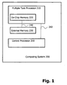
- Fig. 1 is a schematic block diagram illustrating an embodiment of a computing system 200.
- the computing system 200 may be part of a portable device, such as a mobile telephone, a smartphone, a network or data card, or a portable computer.
- the computing system 200 may be an embedded system like a multi-standard mobile chipset and may optionally be realized using one or more ASICs.
- the computing system 200 comprises a multiple task processor 210 having an on-chip memory 220 and an external memory 230 that may be located on a chip different from the chip comprising the multiple task processor 210.
- the external memory 230 is connected to the multiple task processor 210 via a data connection 240.
- the data connection 240 may be realized as a data bus, but could in alternative embodiments also be implemented otherwise.
- the computing system 200 is adapted (e.g., under control of a computer program product) to transfer load module data from the external memory 230 into the on-chip memory 220 in order to generate a load module sequence within the on-chip memory 220.
- the generation of a load module of the load module sequence comprises the following processes: determining which parts of the load module are currently stored within the on-chip memory 220, and transferring only load module data from the external memory 230 into the on-chip memory 220 for parts of the load module which are currently not stored within the on-chip memory 220.
- the computing system 200 is further adapted (e.g., by appropriate control of the multiple task processor 210) to execute the task sequence by running the load module sequence.
- the computing system 200 generates each load module of the load module sequence within an individual address range of the on-chip memory 220 which is chosen in dependence on the load module sequence. Various embodiments for choosing the individual address ranges will be discussed in more detail below.
- the computing system 200 optionally comprises a controi processor 250 which is responsible for loading or initiating loading of the right load module before it is executed.
- the control processor 250 is coupled to the multiple task processor 210 via a command line 260 or otherwise.
- the control processor 250 may be realized as or comprise a memory controller.
- the responsibility of downloading the load module before it is executed may be shared between the control processor 250 and the multiple task processor 210.
- the multiple task processor 210 may be capable of starting and controlling a download of load module data from the external memory 230 into its on-chip program/data memory 220 on its own.
- the control processor 250 may for example ask the multiple task processor 210 to download a complete load module (via a task or a command), but the processor 210 may decide whether a download is actually needed or not, or whether only a part of the load module which has been demanded by the control processor 250 needs to be downloaded or the complete load module, and initiate corresponding actions.
- the actions performed by the multiple task processor 210 may not fully correspond to the commands received from the control processor 250 depending on what load module data is already stored within the on-chip memory 220. This relieves the control processor 250 of the responsibility of low level memory management of the digital signal processor (multiple task processor 210) which can become complex in embedded systems where the multiple task processor 210 typically executes asynchronously.
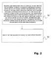
- Fig. 2 shows a flow chart illustrating an embodiment of executing a task on a system comprising a multiple task processor having an on-chip memory and further comprising an external memory connected to the multiple task processor (e.g., as shown in Fig. 1 ).
- an optional initial step it is determined which parts of a load module are currently stored within the on-chip memory.
- step S1 only load module data is transferred from the external memory into the on-chip memory for parts of the load module which are currently not stored within the on-chip memory.
- the load module is generated within an individual address range of the on-chip memory which is chosen in dependence on a load module sequence to be generated within the on-chip memory in accordance with a task sequence to be executed.
- the task is executed by running the load module.
- An advantage of the embodiments illustrated in Figs. 1 and 2 is the fact that, compared to other solutions, the download volume can be decreased. This decrease in download volume leads to lower download times, hence resulting in earlier availability of the result of the tasks, and significant less power consumption. As a consequence, it becomes for example possible to power down the multiple task processor into a low-power dissipation mode or to clock the multiple task processor at a lower -speed leading to lesser power consumption in general.
- generating a load module sequence within the on-chip memory may in particular include the following: in many cases, depending on the number and sizes of load modules and the size of the on-chip memory, some of the load modules may be stored fully, some of the load modules may be stored partly, and some of the load modules may not be stored at all at a given time instance in the on-chip memory.
- the task sequence to be executed may imply a corresponding load module sequence to be run by the multiple task processor and therefore to be available in the on-chip memory.
- load modules may successively be restored (the term "restored” may include: complete the load module by download the missing parts if only a part of the load module is currently stored; fully reload load module if no part of the load module is currently stored; no download if the load module is already fully stored) in the on-chip memory in a unique order implied by the task sequence.
- generating a load module sequence within the on-chip memory may include restoring load modules in the on-chip memory in a unique order implied by the task sequence to be executed.
- the individual address range may in particular include the following: for each load module it may be individually determined which load module start address and which load module end address are preferable in order to decrease the load module download volume. This aspect also includes the case that start addresses or end addresses for different load modules are identical if this nevertheless leads to an overall decrease of the load module download activity.
- the on-chip program memory and the on-chip data memory of the digital signal processor are separate memories.
- execution of a task will require the download of separate load modules for both data memory (data load modules) and program memory (memory load modules).
- data load modules data load modules
- program memory memory load modules
- embodiments of the invention may be applied to downloading data load modules or downloading memory load modules or downloading both data ioad modules and memory ioad modules.
- the program memory and the data memory are condensed into one single memory ("mixed memory").
- a "common" load module may be used for downloading both types of data into the mixed memory. Embodiments are equally applicable to both cases.
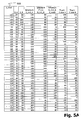
- Fig. 4 shows an embodiment of placing load modules in an on-chip memory 400 having a memory capacity of 120KB as indicated by reference numeral 410.
- the program/data corresponding to a task A is referred to as load module A.
- the program/data corresponding to a task B is referred to as load module B.
- the term "program/data” includes at least one of a set of instructions (i.e., a program) and data to be processed by the program (e.g., constants or variables).
- the memory size of load module A is 60KB, indicated by reference numeral 420, and the memory size of load module B is 90KB, indicated by reference numeral 430. Since the memory capacity of the on-chip memory 300 is not large enough to store both load module A and load module B completely at a time, load module A is overlaid with load module B. In contrast to the embodiment shown in Fig. 3 , each load module is copied such into the on-chip memory 400 that the start addresses of the load modules A and B differ from each other. That is, the start address of module A is 0KB (i.e., coincides with the start address of the on-chip memory 400), whereas the start address of module B is 30KB.
- load module A is only partly overwritten by load module B if load module B is copied into the on-chip memory 400 after having copied load module A into the on-chip memory 400.
- load module B is overwritten by load module A to a lower extent if load module A is copied into the on-chip memory 400 after having copied load module B into the on-chip memory 400.
- every load module may be classified either by START_LEFT (start address of the load module is 0) or by END_RIGHT (end address of load module is end address of on-chip memory 220).
- START_LEFT start address of the load module is 0
- END_RIGHT end address of load module is end address of on-chip memory 220.
- load module A could be classified of the type STAR T LEF T and load module B could be classified of the type END_RIGHT.
- the total memory size of the on-chip memory is denoted by S_Totat, the size of load module A by S_A, and the size of load module B by S_B. Also, it is assumed that S_A + S_B > S_Total (i.e., the on-chip memory is not large enough to simultaneously store load module A and load module B).
- a first scheme (scheme A), that may be based on the memory usage scheme illustrated in Fig. 3 , load module A is loaded completely, and then the programs included within load module A are executed. Then, load module B is loaded completely, and the programs included within load module B are executed. Thus, load module data having a total size of S_A+S_B is downloaded within one cycle. Without loss of generality it is assumed that S_B > S_A and load module A is executed before load module B.
- a second scheme (scheme B) that may also be based on the memory usage scheme illustrated in Fig. 3 , at the first time when load module A is needed, load module A is fully downloaded and then executed. After this, at the first time when load module B is needed, load module B is fully downloaded and then executed. Subsequently, only the intersecting parts of load modules A and B are downloaded, but not the complete load modules A and B.
- Figs. 5A and 5B show, based on some exemplary numbers for S_A, S_B and S_Total, a comparison of the respective performance of schemes A, B and C as described above. As can be derived from Figs. 5A and 5B , scheme C has the best performance.
- Scheme C may take into account scheduling patterns (i.e., the number of different load modules which are executed by the multiple task processor within a particular period of time and the order in which different load modules are executed by the multiple task processor during this period of time). If the number and order of the load modules is known, the location of the respective start addresses and end addresses of the load modules can be chosen such that the overlap between the load modules is minimized.
- scheduling patterns i.e., the number of different load modules which are executed by the multiple task processor within a particular period of time and the order in which different load modules are executed by the multiple task processor during this period of time. If the number and order of the load modules is known, the location of the respective start addresses and end addresses of the load modules can be chosen such that the overlap between the load modules is minimized.
- An optimized arrangement can be obtained by comparing all the possible options against each other. Since the number of load modules within a scheduling period is typically limited, and also since the scheduling sequence of the load modules may be known a priori, comparing all the possible options against each other is not complex.
- the optimized arrangement may be set at the time of linking the code, and not in runtime, hence even if this process should be complex, it can be performed at the time of designing the system.
- load module A size 40KB
- load module B size 60KB
- load module C size 50KB
- Fig. 6 shows a conventional approach of storing load modules within an on-chip memory 600 similar to scheme A illustrated in Fig. 3 .
- the on-chip memory 600 has a memory capacity of 120KB as indicated by reference numeral 610.
- the program/data corresponding to a task A is referred to as load module A.
- the program/data corresponding to a task B is referred to as load module B.
- the program/data corresponding to a task C is referred to as load module C.
- the location of load module A within the on-chip memory 600 is indicated by reference numeral 620
- the location of load module B within the on-chip memory 600 is indicated by reference numeral 630
- the location of load module C within the on-chip memory 600 is indicated by reference numeral 640.
- each load module is copied such into the on-chip memory 600 that a memory start address of the load module always coincides with the memory start address of the on-chip memory 600 (here: start address 0).
- Fig. 7 shows an embodiment of storing load modules within an on-chip memory 700.
- the on-chip memory 700 has a memory capacity of 120KB as indicated by reference numeral 710.
- the program/data corresponding to a task A is referred to as load module A.
- the program/data corresponding to a task B is referred to as load module B.
- the program/data corresponding to a task C is referred to as load module C.
- the location of load module A within the on-chip memory 700 is indicated by reference numeral 720
- the location of load module B within the on-chip memory 700 is indicated by reference numeral 730
- the location of load module C within the on-chip memory 700 is indicated by reference numeral 740.
- load module A is copied such into the on-chip memory 700 that a memory start address of load module A always coincides with the memory start address of the on-chip memory 700 (here: start address 0).
- load module C is copied such into the on-chip memory 700 that a memory start address of load module C is always located immediately after the end address of load module A.
- Load module B is copied such into the on-chip memory 700 that a memory start address of load module B always coincides with the memory start address of the on-chip memory 700 (here: start address 0).
- load module A After having downloaded load module A, load module B, and load module C in this order (initialization period), switching from load module A to load module B requires downloading 60KB, switching from load module B to load module C requires downloading 20KB, and switching from load module C to load module A requires downloading 40KB. Thus, a total load module data of 120KB is needed for one cycle (e.g., one scheduling period).
- the concatenation of load module A and load module C may be (not physically, but logically) interpreted as one load module. This means that the full concatenation of load module A and load module B has to be available regardless of whether only load module A or only load module C has to be executed.
- switching between load modules A and B and switching between load modules C and B, respectively requires 60KB (i.e., switching from load module A to load module B requires downloading 60KB, switching from load module B to load module C requires downloading 60KB. Since load modules A and C are concatenated, there is no switch between load module A and load module C. Hence the total download size is 120 KB.
- Fig. 8 shows a still further embodiment of storing load modules within an on-chip memory 800.
- the on-chip memory 800 has a memory capacity of 120KB as indicated by reference numeral 810.
- the program/data corresponding to a task A is referred to as load module A.
- the program/data corresponding to a task B is referred to as load module B.
- the program/data corresponding to a task C is referred to as load module C.
- the location of load module A within the on-chip memory 800 is indicated by reference numeral 820
- the location of load module B within the on-chip memory 800 is indicated by reference numeral 830
- the location of load module C within the on-chip memory 800 is indicated by reference numeral 840.
- load module A is copied such into the on-chip memory 800 that a memory start address of load module A always coincides with the memory start address of the on-chip memory 800 (here: start address 0).
- load module C is copied such into the on-chip memory 800 that a memory start address of load module C is always located immediately after the end address of load module A.
- Load module B is copied such into the on-chip memory 800 that a memory end address of load module B always coincides with the memory end address of the on-chip memory 800 (here: end address 120KB).
- load module A After having downloaded load module A, load module B, and load module C in this order (initialization period), switching from load module A to load module B requires downloading 30KB, switching from load module B to load module C requires downloading 30KB, and switching from load module C to load module A requires downloading 0KB.
- load module data of 60KB is needed for one cycle (e.g., one scheduling period). Since load modules A and C are logically concatenated, there is no switch between load module C and load module A. Hence, the total download size is 60KB. Generally, after two of the three load modules have been logically concatenated, the two load module download handling example explained earlier can be applied.
- load module A size 60KB
- load module B size 80KB
- load module C size 100KB
- Fig. 9 shows an conventional approach of storing load modules within an on-chip memory 900.
- the on-chip memory 900 has a memory capacity of 120KB as indicated by reference numeral 910.
- the program/data corresponding to a task A is referred to as load module A.
- the program/data corresponding to a task B is referred to as load module B.
- the program/data corresponding to a task C is referred to as load module C.
- the location of load module A within the on-chip memory 900 is indicated by reference numeral 920
- the location of load module B within the on-chip memory 900 is indicated by reference numeral 930
- the location of load module C within the on-chip memory 900 is indicated by reference numeral 940.
- each load module is copied such into the on-chip memory 900 that a memory start address of the load module always coincides with the memory start address of the on-chip memory 900 (here: start address 0).
- start address 0 the memory start address of the on-chip memory 900.
- Fig. 10 shows an embodiment of storing load modules within an on-chip memory 1000.
- the on-chip memory 1000 has a memory capacity of 120KB as indicated by reference numeral 1010.
- the program/data corresponding to a task A is referred to as load module A.
- the program/data corresponding to a task B is referred to as load module B.
- the program/data corresponding to a task C is referred to as load module C.
- the location of load module B within the on-chip memory 1000 is indicated by reference numeral 1020
- the location of load module C within the on-chip memory 1000 is indicated by reference numeral 1030
- the location of load module A within the on-chip memory 1000 is indicated by reference numeral 1040.
- load module B is copied such into the on-chip memory 1000 that a memory start address of load module B always coincides with the memory start address of the on-chip memory 1000 (here: start address 0).
- load module C is copied such into the on-chip memory 1000 that a memory end address of load module C always coincides with the end address of the on-chip memory (here: end address 120).
- load module A is copied such into the on-chip memory 1000 that a memory start address of load module A always coincides with the memory start address of load module C (here: start address 20KB).
- load module data of 180KB is needed for one cycle (e.g., one scheduling period).
- FIG. 11 A comparison between the performance characteristics (download sizes needed) of the embodiments shown in Fig. 9 and Fig. 10 is summarized in Fig. 11 .
- the embodiment illustrated in Fig. 10 significantly reduces the download volume compared to the scenario shown in Fig. 9 (180 KB vs. 220 KB).
- a load module directory of active and valid load modules is maintained in the on-chip memory 220 or in another place (see Fig. 1 ).
- the number of maintained modules is 2 (load module A or LM1 and load module B or LM2).
- any number of load modules may be maintained.
- the load module directory is invalidated (initialized) at booting time. After this, both load module A and load module B are fully downloaded (with start addresses chosen based upon scheme C for example).
- load module A or load module B only "corrupted” parts (i.e., the overlapping region between load module A and load module B) are downloaded (or “repaired”).
- a load module is called active if it has already been completely downloaded once.
- a load module is called valid if it is active and no part of it is corrupted. It is possible that a load module is active but not valid, but a load module cannot be valid if it is not active.
- a DSP may check if the load module to be downloaded is already active by looking up the load module directory. Based upon the start and end address as well as the status of the load module (represented by, for example, active/valid flags assigned to the load module or other status indicators), the download is started to repair the corrupted parts.
- the load module is fully downloaded to the requested address in the on-chip memory 220 (also called Tightly Coupled Memory, or TCM).
- TCM Tightly Coupled Memory
- This download may also be tied to a DMA callback action that registers the tasks present inside the downloaded dynamic load module with the execution platform of the multiple task processor 210.Once the DMA is completed, an interrupt may be raised to the digital signal processor. In response to that interrupt, the DSP may update the load module tables that it maintains internally. The invalidation of the other load modules should be done before the download is started for the load module of interest.
- step 1202 the process is started.
- a DSP which may realize the multiple task processor 210 of Fig. 1 is asked (e.g., by an application program) to download load module A having load module descriptor A.
- the DSP or a memory controller looks into the load module directory in order to obtain information about load module A.
- step 1208 it is determined whether load module A is active. If it is determined that the load module A is not active, load module B is marked as invalid at step 1224 and the complete load module A is downloaded at step 1212. After this, at step 1218, load module A is e marked as active and valid.Then, at step 1220, the task directory is updated based on the load module descriptor of load module A, and the process is ended at step 1222.
- step 1210 determines whether load module A is valid. If it is determined at step 1210 that load module A is valid, it is decided at step 1216 that nothing has to be downloaded, and the process is ended at step 1222. If, on the other hand, it is determined at step 1210 that load module A is not valid, then load module B is marked as invalid at step 1226 and the corrupted parts of load module A are downloaded at step 1214. Then, at step 1218, load module A is marked as active and valid. Next, at step 1220, the task directory is updated based on the load module descriptor of load module A, and the process is ended at step 1222. The situation is handled in an inversely manner if, at step 1204, it is asked to download load module B.
- Fig. 13 The process described above with reference to Fig. 12 is also reflected by Fig. 13 as a seven step procedure.
- Fig. 13 the individual triggering events and the respective DMA responses are illustrated.
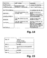
- Fig. 14 shows an embodiment of a load module descriptor. Every load module may include a load module descriptor that may be associated with one or more (or each) load module. As an example, the load module descriptor may be stored (e.g., in the on-chip memory) together with the load module. Load module descriptor data may be used to create DMA descriptors that can be used to download the load module to the TCM.
- the load module descriptor may, for example, be represented by the following data structure (the meaning of the data items is explained in the comment section of Fig. 14 ):
- Fig. 15 shows an embodiment of a task table which may be used (via a pointer) as an element of the load module descriptor shown in Fig. 14 .
- the task table may be maintained by an execution platform (equivalent of an operating system) that executes on the DSP
- the task table comprises a list of the tasks that are included within the load module represented by the load module descriptor.
- Fig. 16 shows a comparison between task execution times on two computing systems.
- Reference numeral 1602 shows a time chart for a computing system having a cache
- reference numeral 1604 for a computing system having no cache, but an on-chip memory management as explained above. It is assumed that in a time period (unit granularity for scheduling), two tasks are executed on the processor: Task T1 that needs load module 1 (LM1), and task T2 that needs load module 2 (LM2). It can be derived from Fig. 16 that the latency in the availability of task T1 and task T2 is decreased for computing system 1604.
- LM1 load module 1
- LM2 load module 2
- Task scheduling information available in advance may be used to optimize the performance of the memory management of the muitipie task processor (see reference numeral 210 in Fig. 1 ). That is, the order of the tasks to be executed and thus the corresponding order of load modules to be run may serve as a basis for determining which start addresses and end addresses should be used for the load modules in order to reduce the amount of downloaded load module data.
- information pertaining to the sequence in which the load modules are utilized on the multiple task processor along with their sizes may be used to optimally manage the on-chip memory of the multiple processor. This information is available in many multiple task processors since systems that can typically make use of the above embodiments may have very tight real time constraints and deadlines for the processing.
- a technique for optimal usage of the program/data memory is provided which is shared between multiple tasks.
- This technique allows reducing the size of the on-chip memory which may ultimately result in the reduction of the size of the die on which the multiple task processor is manufactured. This reduction is a requirement for mobile handsets and many other embedded systems.
- the traffic on memory buses is significantly reduced. This reduces the power consumption in the embedded system.
- the download volume can be decreased. This decrease in download volume leads to lower download times, hence resulting in earlier availability of the result of a task, and significant less power consumption. As a consequence, it becomes for example possible to power down the multiple task processor into a low-power dissipation mode or to clock the multiple task processor at a lower speed leading to less power consumption in general.
- the multiple task processor can be (more often) set into a low power mode which will reduce the power consumption in the device.
- the multiple task processor can be (more often) clocked at a lower rate that will reduce the power consumption of the device.
- embodiments of the technique presented herein may be used for memory optimization on processors without cache memory (cache memory would require that the processor architecture is designed with a cache).
- the embodiments may be implemented as software which is cheap to realize.
- the multiple task processor may be aware and partly be responsible (shares memory management responsibility with the control processor) for its own memory management.
- only the size of the load modules may be used as input parameter for optimization of the on-chip memory management.
- a further advantage of certain embodiments is the fact that the on-chip memory management does not lead to any uncertainty in load module execution time.
- the on-chip memory update operation may be decoupled from accessing the memory by the multiple task processor. This approach allows that the memory update can be considered for the scheduling on the processor.
- the on-chip memory update can be performed when the processor load is low (these times are usually known to the control processor which is responsible for initiating the download of the correct load module for the task, so the control processor can initiate the memory updates at the right times).
- Certain embodiments may not need hardware support which is for example needed for virtual memory, typically in the form of a Memory Management Unit (MMU). Still further, in certain embodiments an optimization can be used to place the load modules at optimum locations in the process memory space (on-chip memory) at compile and link time. By using the knowledge of scheduling on the multiple task processor, performance optimization is possible.
- MMU Memory Management Unit
- the start/end addresses of the load modules may correspond to physical addresses of the on-chip memory.
- the on-chip memory may be a TCM comprising program tightly coupled memory (PCTM) and/or data tightly coupled memory (DTCM). Deterministic patterns in the scheduling of tasks on the processor may be used for on-chip memory optimization.
Landscapes
- Engineering & Computer Science (AREA)
- Software Systems (AREA)
- Theoretical Computer Science (AREA)
- Physics & Mathematics (AREA)
- General Engineering & Computer Science (AREA)
- General Physics & Mathematics (AREA)
- Stored Programmes (AREA)
Claims (20)
- Procédé pour exécuter une séquence de tâches sur un système (200) comprenant un processeur de tâches multiples (210) ayant une mémoire sur puce (220,300,400,600,700,800,900,1000) et une mémoire externe (230) connectée au processeur de tâches multiples (210), le procédé comprenant de :- transférer des données de module de charge à partir de la mémoire externe (230) sur la mémoire sur puce (220) de manière à générer une séquence de module de charge à l'intérieur de la mémoire sur puce (220), dans lequel un module de charge inclut au moins un d'un programme et de données à traiter par le programme, et dans lequel la génération d'un module de charge de la séquence de module de charge comprend les processus suivants : déterminer, sur la base des adresses de début sur puce et des adresses de fin sur puce respectives des modules de charge de la séquence de module de charge, sur la base d'un premier indicateur indiquant si le module de charge a déjà été complètement chargé au moins une fois dans la mémoire sur puce (220), et sur la base d'un second indicateur indiquant si au moins une partie du module de charge, après avoir été complètement chargé dans la mémoire sur puce (220), est actuellement en train d'être écrasée, lesquelles parties du module de charge sont actuellement mémorisées à l'intérieur de la mémoire sur puce (220), et transférer seulement les données de module de charge de la mémoire externe (230) dans la mémoire sur puce (220) pour les parties du module de charge qui ne sont actuellement par mémorisées dans la mémoire sur puce (220) si le premier indicateur est dans un état FALSE ou dans lequel le module de charge est partiellement chargé dans la mémoire sur puce (220) si le premier indicateur est dans un état TRUE et le second indicateur est dans un état FALSE, ou dans lequel aucune partie du module de charge n'est chargée dans la mémoire sur puce (220) si le premier indicateur et le second indicateur sont respectivement dans un état TRUE, dans lequel chaque module de charge de la séquence de module de charge est générée à l'intérieur d'une plage d'adresses individuelles de la mémoire sur puce (220) qui est choisi en fonction de la séquence de module de charge, et- exécuter la séquence de tâches en exécutant la séquence de module de charge.
- Procédé selon la revendication 1, dans lequel les plages d'adresses des modules de charge de la séquence de module de charge sont choisies de telle sorte que la quantité de données de module de charge transférées de la mémoire externe (230) dans la mémoire sur puce (220) soit minimisée.
- Procédé selon la revendication 1 ou 2, dans lequel au moins une des adresses de début sur puce et des adresses de fin sur puce des plages d'adresses des modules de charge sont choisies en fonction d'un ou des deux de la taille des modules de charge et de l'ordre selon lequel les modules de charge sont générés à l'intérieur de la mémoire sur puce (220).
- Procédé selon une quelconque des revendications 1 à 3, dans lequel au moins une des adresses de début sur puce et des adresses de fin sur puce des modules de charge à l'intérieur de la mémoire sur puce (220) sont choisies de telle sorte que la plus grande partie possible de la plage d'adresses de mémoire sur puce (220) soit couverte par les modules de charge.
- Procédé selon une quelconque des revendications 1 à 4, dans lequel au moins une des adresses de début sur puce et des adresses de fin sur puce des modules de charge à l'intérieur de la mémoire sur puce (220) sont choisis de telle sorte que,- au cas où la somme des longueurs de données des modules de charge déjà générés à l'intérieur de la mémoire sur puce (220) est plus petite que la taille de données totale de la mémoire sur puce (220), les plages d'adresses des données de module de charge de différentes modules de charge ne se superposent pas les unes aux autres, ou- au cas où la somme des longueurs de données des modules de charge déjà générés à l'intérieur de la mémoire sur puce (220) est plus grande que la taille de données totale de la mémoire sur puce (220), la plage d'adresses totale de la mémoire sur puce est couverte par les données de module de charge des modules de charge.
- Procédé selon une quelconque des revendications 1 à 5, comprenant en outre de :générer successivement des modules de charge à l'intérieur de la mémoire sur puce (220), dans lequel une adresse de début assignée à un module de charge actuellement généré à l'intérieur de la mémoire sur puce (220) est situé immédiatement après l'adresse de fin sur puce d'un module de charge généré précédemment, dans lequel, dès que la somme des longueurs de données des modules de charge déjà générés à l'intérieur de la mémoire sur puce (220) et d'un autre module de charge à générer excède la taille de données totale de la mémoire sur puce (220), assigner une adresse de fin sur puce à l'autre module de charge qui coïncide avec l'adresse la plus haute de la mémoire sur puce (220).
- Procédé selon la revendication 6, dans lequel une adresse de début sur puce assignée à un premier module de charge généré à l'intérieur de la mémoire sur puce (220) coïncide avec l'adresse la plus basse de la mémoire sur puce (220).
- Procédé selon une quelconque des revendications 1 à 7, dans lequel la détermination de quelles parties du module de charge sont actuellement mémorisées à l'intérieur de la mémoire sur puce et/ou quelles données de module doivent être téléchargées est au moins partiellement commandé par le processeur de tâches multiples.
- Procédé selon une quelconque des revendications 1 à 8, dans lequel le processeur de tâches multiples (210) est un processeur de signaux numériques.
- Produit de programme informatique comprenant des portions de code de programme pour mettre en oeuvre les étapes d'une quelconque des revendications 1 à 9 quand le produit de programme informatique est exécuté sur un dispositif informatique.
- Produit de programme informatique selon la revendication 10, mémorisé sur un support d'enregistrement lisible par ordinateur.
- Système informatique (200) comprenant un processeur de tâches multiples (210) ayant une mémoire sur puce (220,300,400,600,700,800,900,1000) et comprenant en outre une mémoire externe (230) connectée au processeur de tâches multiples (210), le système informatique (200) étant adapté afin de :- transférer des données de module de charge à partir de la mémoire externe (230) sur la mémoire sur puce (220) de manière à générer une séquence de module de charge à l'intérieur de la mémoire sur puce (220), dans lequel un module de charge inclut au moins un d'un programme et de données à traiter par le programme, et dans lequel la génération d'un module de charge de la séquence de module de charge comprend les processus suivants : déterminer, sur la base des adresses de début sur puce et des adresses de fin sur puce respectives des modules de charge de la séquence de module de charge, sur la base d'un premier indicateur indiquant si le module de charge a déjà été complètement chargé au moins une fois dans la mémoire sur puce (220), et sur la base d'un second indicateur indiquant si au moins une partie du module de charge, après avoir été complètement chargé dans la mémoire sur puce (220), est actuellement en train d'être écrasée, lesquelles parties du module de charge sont actuellement mémorisées à l'intérieur de la mémoire sur puce (220), et transférer seulement les données de module de charge de la mémoire externe (230) dans la mémoire sur puce (220) pour les parties du module de charge qui ne sont actuellement par mémorisées dans la mémoire sur puce (220) si le premier indicateur est dans un état FALSE ou dans lequel le module de charge est partiellement chargé dans la mémoire sur puce (220) si le premier indicateur est dans un état TRUE et le second indicateur est dans un état FALSE, ou dans lequel aucune partie du module de charge n'est chargée dans la mémoire sur puce (220) si le premier indicateur et le second indicateur sont respectivement dans un état TRUE, et- exécuter la séquence de tâches en exécutant la séquence de module de charge, dans lequel le système informatique (200) est en outre adapté afin de générer chaque module de charge de la séquence de module de charge à l'intérieur d'une plage d'adresses individuelles de la mémoire sur puce (220) qui est choisie en fonction de la séquence de module de charge.
- Système informatique (200) selon la revendication 12, le système informatique (200) étant adapté afin de choisir les plages d'adresses de modules de charge de la séquence de module de charge de sorte que la quantité des données de module de charge transférées de la mémoire externe (230) dans la mémoire sur puce (220) soit minimisée.
- Système informatique selon la revendication 12 ou 13, le système informatique (200) étant adapté afin de choisir au moins une d'adresses de début sur puce et d'adresses de fin sur puce des plages d'adresse des modules de charge en fonction d'un ou des deux de la taille de modules de charge et de l'ordre selon lequel les modules de charge sont générés à l'intérieur de la mémoire sur puce (220).
- Système informatique (200) selon une quelconque des revendications 12 à 14, le système informatique (200) étant adapté afin de choisir au moins une adresses de début sur puce et des adresses de fin sur puce des modules de charge à l'intérieur de la mémoire sur puce (220) de sorte que la plus grande partie possible de la plage d'adresses de mémoire sur puce (220) soit couverte par les modules de charge.
- Système informatique (200) selon une quelconque des revendications 12 à 14, le système informatique (200) étant adapté afin de choisir au moins une des adresses de début sur puce et des adresses de fin sur puce des modules de charge à l'intérieur de la mémoire sur puce (220), de sorte que,- au cas où la somme des longueurs de données des modules de charge déjà générés à l'intérieur de la mémoire sur puce (220) est plus petite que la taille de données totale de la mémoire sur puce (220), les plages d'adresses des données de module de charge de différentes modules de charge ne se superposent pas les unes aux autres, ou- au cas où la somme des longueurs de données des modules de charge déjà générés à l'intérieur de la mémoire sur puce (220) est plus grande que la taille de données totale de la mémoire sur puce (220), la plage d'adresses totale de la mémoire sur puce (220) est couverte par les données de module de charge des modules de charge.
- Système informatique (200) selon une quelconque des revendications 12 à 16, le système informatique (200) étant adapté afin de générer successivement les modules de charge à l'intérieur de la mémoire sur puce (220), dans lequel une adresse de début sur puce assigné à un module de charge actuellement généré à l'intérieur de la mémoire sur puce (220) est située immédiatement après l'adresse de fin sur puce d'un module de charge précédemment généré, dans lequel, dès que la somme des longueurs de données des modules de charge déjà générés à l'intérieur de la mémoire sur puce (220) et d'un autre module de charge à générer excède la taille de données totale de la mémoire sur puce (220), assigner une adresse de fin sur puce à l'autre module de charge qui coïncide avec l'adresse la plus haute de la mémoire sur puce (220).
- Système informatique (200) selon la revendication 17, dans lequel une adresse de début sur puce assignée à un premier module de charge généré à l'intérieur de la mémoire sur puce (220) coïncide avec l'adresse la plus basse de la mémoire sur puce (220).
- Système informatique (200) selon une quelconque des revendications 12 à 18, dans lequel le processeur de tâches multiples (210) est adapté afin de commander au moins partiellement quelles parties des modules de charge sont actuellement mémorisées à l'intérieur de la mémoire sur puce (220) et/ou quel type de données de module doit être téléchargé.
- Système informatique (200) selon une quelconque des revendications 12 à 19, dans lequel le processeur de tâches multiples (210) est un processeur de signaux numériques.
Priority Applications (3)
| Application Number | Priority Date | Filing Date | Title |
|---|---|---|---|
| EP11005362.6A EP2541404B1 (fr) | 2011-06-30 | 2011-06-30 | Technique pour l'exécution de séquence de tâche |
| PCT/EP2012/002685 WO2013000564A1 (fr) | 2011-06-30 | 2012-06-26 | Technique d'exécution de séquences de tâches |
| US14/128,115 US20140137126A1 (en) | 2011-06-30 | 2012-06-26 | Technique for Task Sequence Execution |
Applications Claiming Priority (1)
| Application Number | Priority Date | Filing Date | Title |
|---|---|---|---|
| EP11005362.6A EP2541404B1 (fr) | 2011-06-30 | 2011-06-30 | Technique pour l'exécution de séquence de tâche |
Publications (2)
| Publication Number | Publication Date |
|---|---|
| EP2541404A1 EP2541404A1 (fr) | 2013-01-02 |
| EP2541404B1 true EP2541404B1 (fr) | 2014-08-13 |
Family
ID=46397149
Family Applications (1)
| Application Number | Title | Priority Date | Filing Date |
|---|---|---|---|
| EP11005362.6A Not-in-force EP2541404B1 (fr) | 2011-06-30 | 2011-06-30 | Technique pour l'exécution de séquence de tâche |
Country Status (3)
| Country | Link |
|---|---|
| US (1) | US20140137126A1 (fr) |
| EP (1) | EP2541404B1 (fr) |
| WO (1) | WO2013000564A1 (fr) |
Families Citing this family (4)
| Publication number | Priority date | Publication date | Assignee | Title |
|---|---|---|---|---|
| US10101992B2 (en) * | 2015-06-15 | 2018-10-16 | Lear Corporation | Telematics control unit comprising a differential update package |
| CN109522101B (zh) * | 2017-09-20 | 2023-11-14 | 三星电子株式会社 | 用于调度多个操作系统任务的方法、系统和/或装置 |
| JP7367365B2 (ja) * | 2019-07-23 | 2023-10-24 | 富士通株式会社 | タスク実行管理装置、タスク実行管理方法、および、タスク実行管理プログラム |
| CN111371705B (zh) * | 2020-02-24 | 2023-09-12 | 维沃移动通信有限公司 | 一种下载任务执行方法及电子设备 |
Family Cites Families (10)
| Publication number | Priority date | Publication date | Assignee | Title |
|---|---|---|---|---|
| US6026471A (en) * | 1996-11-19 | 2000-02-15 | International Business Machines Corporation | Anticipating cache memory loader and method |
| US6167488A (en) * | 1997-03-31 | 2000-12-26 | Sun Microsystems, Inc. | Stack caching circuit with overflow/underflow unit |
| US6427192B1 (en) * | 1998-09-21 | 2002-07-30 | Advanced Micro Devices, Inc. | Method and apparatus for caching victimized branch predictions |
| JP3973129B2 (ja) * | 2000-07-19 | 2007-09-12 | 株式会社日立製作所 | キャッシュメモリ装置及びそれを用いた中央演算処理装置 |
| US7124276B2 (en) * | 2003-04-14 | 2006-10-17 | Broadcom Corporation | Optimizing cache efficiency within application software |
| JP4837247B2 (ja) * | 2003-09-24 | 2011-12-14 | パナソニック株式会社 | プロセッサ |
| US7428645B2 (en) * | 2003-12-29 | 2008-09-23 | Marvell International, Ltd. | Methods and apparatus to selectively power functional units |
| US7496908B2 (en) * | 2004-01-14 | 2009-02-24 | International Business Machines Corporation | Method and apparatus for optimizing code execution using annotated trace information having performance indicator and counter information |
| US8458380B2 (en) * | 2008-03-26 | 2013-06-04 | Qualcomm Incorporated | Off-line task list architecture utilizing tightly coupled memory system |
| US8086804B2 (en) * | 2008-09-24 | 2011-12-27 | Oracle America, Inc. | Method and system for optimizing processor performance by regulating issue of pre-fetches to hot cache sets |
-
2011
- 2011-06-30 EP EP11005362.6A patent/EP2541404B1/fr not_active Not-in-force
-
2012
- 2012-06-26 US US14/128,115 patent/US20140137126A1/en not_active Abandoned
- 2012-06-26 WO PCT/EP2012/002685 patent/WO2013000564A1/fr not_active Ceased
Also Published As
| Publication number | Publication date |
|---|---|
| US20140137126A1 (en) | 2014-05-15 |
| EP2541404A1 (fr) | 2013-01-02 |
| WO2013000564A1 (fr) | 2013-01-03 |
Similar Documents
| Publication | Publication Date | Title |
|---|---|---|
| US7765391B2 (en) | Multiprocessor system and boot-up method of slave system | |
| US9043806B2 (en) | Information processing device and task switching method | |
| JPWO2009157178A1 (ja) | 仮想計算機制御装置、仮想計算機制御プログラム及び仮想計算機制御回路 | |
| CN105765541A (zh) | 用于机动车的控制器 | |
| WO2016099820A1 (fr) | Mécanisme de rappel de fonction amélioré entre une unité centrale de traitement (cpu) et un processeur auxiliaire | |
| EP4287023B1 (fr) | Procédé et dispositif de traitement de service | |
| CN116521324B (zh) | 中断虚拟化处理方法、装置及电子设备 | |
| CN104932933A (zh) | 一种获取自旋锁的方法及装置 | |
| JP2017097633A (ja) | 車両制御装置 | |
| EP2541404A1 (fr) | Technique pour l'exécution de séquence de tâche | |
| JP4151198B2 (ja) | 割込コントローラ及びマイクロコンピュータ | |
| US8751703B2 (en) | Interrupt event management | |
| CN115437696A (zh) | 信创平台自适应配置方法及终端助手 | |
| US8924697B2 (en) | Method for processing interrupt requests in a processor | |
| RU2554569C2 (ru) | Устройство для загрузки интегральной схемы soc и интегральная схема типа soc | |
| JP2014191655A (ja) | マルチプロセッサ、電子制御装置、プログラム | |
| JP2004516547A (ja) | 中断制御装置 | |
| JP6654230B2 (ja) | 車両制御装置 | |
| US20080052485A1 (en) | System For Synchronous Code Retrieval From An Asynchronous Source | |
| JP2009258984A (ja) | 情報処理装置およびロード制御方法 | |
| CN116483643A (zh) | 一种gpu调试方法、装置、设备及存储介质 | |
| EP3428799B1 (fr) | Dispositif d'accès de données et procédé de notification d'erreurs d'accès | |
| CN102508681B (zh) | 多核系统不中断业务的补丁方法及系统 | |
| CN121326815B (zh) | 加速设备、系统及方法 | |
| CN113010236A (zh) | 一种程序执行方法、装置、设备及存储介质 |
Legal Events
| Date | Code | Title | Description |
|---|---|---|---|
| PUAI | Public reference made under article 153(3) epc to a published international application that has entered the european phase |
Free format text: ORIGINAL CODE: 0009012 |
|
| 17P | Request for examination filed |
Effective date: 20120521 |
|
| AK | Designated contracting states |
Kind code of ref document: A1 Designated state(s): AL AT BE BG CH CY CZ DE DK EE ES FI FR GB GR HR HU IE IS IT LI LT LU LV MC MK MT NL NO PL PT RO RS SE SI SK SM TR |
|
| AX | Request for extension of the european patent |
Extension state: BA ME |
|
| 17Q | First examination report despatched |
Effective date: 20130109 |
|
| GRAP | Despatch of communication of intention to grant a patent |
Free format text: ORIGINAL CODE: EPIDOSNIGR1 |
|
| INTG | Intention to grant announced |
Effective date: 20140320 |
|
| GRAS | Grant fee paid |
Free format text: ORIGINAL CODE: EPIDOSNIGR3 |
|
| GRAA | (expected) grant |
Free format text: ORIGINAL CODE: 0009210 |
|
| AK | Designated contracting states |
Kind code of ref document: B1 Designated state(s): AL AT BE BG CH CY CZ DE DK EE ES FI FR GB GR HR HU IE IS IT LI LT LU LV MC MK MT NL NO PL PT RO RS SE SI SK SM TR |
|
| REG | Reference to a national code |
Ref country code: GB Ref legal event code: FG4D |
|
| REG | Reference to a national code |
Ref country code: CH Ref legal event code: EP Ref country code: AT Ref legal event code: REF Ref document number: 682588 Country of ref document: AT Kind code of ref document: T Effective date: 20140815 |
|
| REG | Reference to a national code |
Ref country code: IE Ref legal event code: FG4D |
|
| REG | Reference to a national code |
Ref country code: DE Ref legal event code: R096 Ref document number: 602011008980 Country of ref document: DE Effective date: 20140925 |
|
| REG | Reference to a national code |
Ref country code: NL Ref legal event code: VDEP Effective date: 20140813 |
|
| REG | Reference to a national code |
Ref country code: AT Ref legal event code: MK05 Ref document number: 682588 Country of ref document: AT Kind code of ref document: T Effective date: 20140813 |
|
| REG | Reference to a national code |
Ref country code: LT Ref legal event code: MG4D |
|
| PG25 | Lapsed in a contracting state [announced via postgrant information from national office to epo] |
Ref country code: PT Free format text: LAPSE BECAUSE OF FAILURE TO SUBMIT A TRANSLATION OF THE DESCRIPTION OR TO PAY THE FEE WITHIN THE PRESCRIBED TIME-LIMIT Effective date: 20141215 Ref country code: BG Free format text: LAPSE BECAUSE OF FAILURE TO SUBMIT A TRANSLATION OF THE DESCRIPTION OR TO PAY THE FEE WITHIN THE PRESCRIBED TIME-LIMIT Effective date: 20141113 Ref country code: FI Free format text: LAPSE BECAUSE OF FAILURE TO SUBMIT A TRANSLATION OF THE DESCRIPTION OR TO PAY THE FEE WITHIN THE PRESCRIBED TIME-LIMIT Effective date: 20140813 Ref country code: SE Free format text: LAPSE BECAUSE OF FAILURE TO SUBMIT A TRANSLATION OF THE DESCRIPTION OR TO PAY THE FEE WITHIN THE PRESCRIBED TIME-LIMIT Effective date: 20140813 Ref country code: GR Free format text: LAPSE BECAUSE OF FAILURE TO SUBMIT A TRANSLATION OF THE DESCRIPTION OR TO PAY THE FEE WITHIN THE PRESCRIBED TIME-LIMIT Effective date: 20141114 Ref country code: ES Free format text: LAPSE BECAUSE OF FAILURE TO SUBMIT A TRANSLATION OF THE DESCRIPTION OR TO PAY THE FEE WITHIN THE PRESCRIBED TIME-LIMIT Effective date: 20140813 Ref country code: LT Free format text: LAPSE BECAUSE OF FAILURE TO SUBMIT A TRANSLATION OF THE DESCRIPTION OR TO PAY THE FEE WITHIN THE PRESCRIBED TIME-LIMIT Effective date: 20140813 Ref country code: NO Free format text: LAPSE BECAUSE OF FAILURE TO SUBMIT A TRANSLATION OF THE DESCRIPTION OR TO PAY THE FEE WITHIN THE PRESCRIBED TIME-LIMIT Effective date: 20141113 |
|
| PG25 | Lapsed in a contracting state [announced via postgrant information from national office to epo] |
Ref country code: AT Free format text: LAPSE BECAUSE OF FAILURE TO SUBMIT A TRANSLATION OF THE DESCRIPTION OR TO PAY THE FEE WITHIN THE PRESCRIBED TIME-LIMIT Effective date: 20140813 Ref country code: CY Free format text: LAPSE BECAUSE OF FAILURE TO SUBMIT A TRANSLATION OF THE DESCRIPTION OR TO PAY THE FEE WITHIN THE PRESCRIBED TIME-LIMIT Effective date: 20140813 Ref country code: IS Free format text: LAPSE BECAUSE OF FAILURE TO SUBMIT A TRANSLATION OF THE DESCRIPTION OR TO PAY THE FEE WITHIN THE PRESCRIBED TIME-LIMIT Effective date: 20141213 Ref country code: HR Free format text: LAPSE BECAUSE OF FAILURE TO SUBMIT A TRANSLATION OF THE DESCRIPTION OR TO PAY THE FEE WITHIN THE PRESCRIBED TIME-LIMIT Effective date: 20140813 Ref country code: RS Free format text: LAPSE BECAUSE OF FAILURE TO SUBMIT A TRANSLATION OF THE DESCRIPTION OR TO PAY THE FEE WITHIN THE PRESCRIBED TIME-LIMIT Effective date: 20140813 Ref country code: LV Free format text: LAPSE BECAUSE OF FAILURE TO SUBMIT A TRANSLATION OF THE DESCRIPTION OR TO PAY THE FEE WITHIN THE PRESCRIBED TIME-LIMIT Effective date: 20140813 |
|
| PG25 | Lapsed in a contracting state [announced via postgrant information from national office to epo] |
Ref country code: NL Free format text: LAPSE BECAUSE OF FAILURE TO SUBMIT A TRANSLATION OF THE DESCRIPTION OR TO PAY THE FEE WITHIN THE PRESCRIBED TIME-LIMIT Effective date: 20140813 |
|
| PG25 | Lapsed in a contracting state [announced via postgrant information from national office to epo] |
Ref country code: RO Free format text: LAPSE BECAUSE OF FAILURE TO SUBMIT A TRANSLATION OF THE DESCRIPTION OR TO PAY THE FEE WITHIN THE PRESCRIBED TIME-LIMIT Effective date: 20140813 Ref country code: SK Free format text: LAPSE BECAUSE OF FAILURE TO SUBMIT A TRANSLATION OF THE DESCRIPTION OR TO PAY THE FEE WITHIN THE PRESCRIBED TIME-LIMIT Effective date: 20140813 Ref country code: DK Free format text: LAPSE BECAUSE OF FAILURE TO SUBMIT A TRANSLATION OF THE DESCRIPTION OR TO PAY THE FEE WITHIN THE PRESCRIBED TIME-LIMIT Effective date: 20140813 Ref country code: EE Free format text: LAPSE BECAUSE OF FAILURE TO SUBMIT A TRANSLATION OF THE DESCRIPTION OR TO PAY THE FEE WITHIN THE PRESCRIBED TIME-LIMIT Effective date: 20140813 Ref country code: IT Free format text: LAPSE BECAUSE OF FAILURE TO SUBMIT A TRANSLATION OF THE DESCRIPTION OR TO PAY THE FEE WITHIN THE PRESCRIBED TIME-LIMIT Effective date: 20140813 Ref country code: CZ Free format text: LAPSE BECAUSE OF FAILURE TO SUBMIT A TRANSLATION OF THE DESCRIPTION OR TO PAY THE FEE WITHIN THE PRESCRIBED TIME-LIMIT Effective date: 20140813 |
|
| REG | Reference to a national code |
Ref country code: DE Ref legal event code: R097 Ref document number: 602011008980 Country of ref document: DE |
|
| PG25 | Lapsed in a contracting state [announced via postgrant information from national office to epo] |
Ref country code: PL Free format text: LAPSE BECAUSE OF FAILURE TO SUBMIT A TRANSLATION OF THE DESCRIPTION OR TO PAY THE FEE WITHIN THE PRESCRIBED TIME-LIMIT Effective date: 20140813 |
|
| PLBE | No opposition filed within time limit |
Free format text: ORIGINAL CODE: 0009261 |
|
| STAA | Information on the status of an ep patent application or granted ep patent |
Free format text: STATUS: NO OPPOSITION FILED WITHIN TIME LIMIT |
|
| 26N | No opposition filed |
Effective date: 20150515 |
|
| PG25 | Lapsed in a contracting state [announced via postgrant information from national office to epo] |
Ref country code: SI Free format text: LAPSE BECAUSE OF FAILURE TO SUBMIT A TRANSLATION OF THE DESCRIPTION OR TO PAY THE FEE WITHIN THE PRESCRIBED TIME-LIMIT Effective date: 20140813 |
|
| PG25 | Lapsed in a contracting state [announced via postgrant information from national office to epo] |
Ref country code: MC Free format text: LAPSE BECAUSE OF FAILURE TO SUBMIT A TRANSLATION OF THE DESCRIPTION OR TO PAY THE FEE WITHIN THE PRESCRIBED TIME-LIMIT Effective date: 20140813 |
|
| REG | Reference to a national code |
Ref country code: CH Ref legal event code: PL |
|
| GBPC | Gb: european patent ceased through non-payment of renewal fee |
Effective date: 20150630 |
|
| PG25 | Lapsed in a contracting state [announced via postgrant information from national office to epo] |
Ref country code: LU Free format text: LAPSE BECAUSE OF FAILURE TO SUBMIT A TRANSLATION OF THE DESCRIPTION OR TO PAY THE FEE WITHIN THE PRESCRIBED TIME-LIMIT Effective date: 20150630 |
|
| REG | Reference to a national code |
Ref country code: IE Ref legal event code: MM4A |
|
| REG | Reference to a national code |
Ref country code: FR Ref legal event code: ST Effective date: 20160229 |
|
| PG25 | Lapsed in a contracting state [announced via postgrant information from national office to epo] |
Ref country code: GB Free format text: LAPSE BECAUSE OF NON-PAYMENT OF DUE FEES Effective date: 20150630 Ref country code: LI Free format text: LAPSE BECAUSE OF NON-PAYMENT OF DUE FEES Effective date: 20150630 Ref country code: IE Free format text: LAPSE BECAUSE OF NON-PAYMENT OF DUE FEES Effective date: 20150630 Ref country code: CH Free format text: LAPSE BECAUSE OF NON-PAYMENT OF DUE FEES Effective date: 20150630 |
|
| PG25 | Lapsed in a contracting state [announced via postgrant information from national office to epo] |
Ref country code: FR Free format text: LAPSE BECAUSE OF NON-PAYMENT OF DUE FEES Effective date: 20150630 |
|
| PG25 | Lapsed in a contracting state [announced via postgrant information from national office to epo] |
Ref country code: BE Free format text: LAPSE BECAUSE OF FAILURE TO SUBMIT A TRANSLATION OF THE DESCRIPTION OR TO PAY THE FEE WITHIN THE PRESCRIBED TIME-LIMIT Effective date: 20140813 |
|
| PG25 | Lapsed in a contracting state [announced via postgrant information from national office to epo] |
Ref country code: MT Free format text: LAPSE BECAUSE OF FAILURE TO SUBMIT A TRANSLATION OF THE DESCRIPTION OR TO PAY THE FEE WITHIN THE PRESCRIBED TIME-LIMIT Effective date: 20140813 |
|
| PG25 | Lapsed in a contracting state [announced via postgrant information from national office to epo] |
Ref country code: SM Free format text: LAPSE BECAUSE OF FAILURE TO SUBMIT A TRANSLATION OF THE DESCRIPTION OR TO PAY THE FEE WITHIN THE PRESCRIBED TIME-LIMIT Effective date: 20140813 Ref country code: HU Free format text: LAPSE BECAUSE OF FAILURE TO SUBMIT A TRANSLATION OF THE DESCRIPTION OR TO PAY THE FEE WITHIN THE PRESCRIBED TIME-LIMIT; INVALID AB INITIO Effective date: 20110630 |
|
| PG25 | Lapsed in a contracting state [announced via postgrant information from national office to epo] |
Ref country code: TR Free format text: LAPSE BECAUSE OF FAILURE TO SUBMIT A TRANSLATION OF THE DESCRIPTION OR TO PAY THE FEE WITHIN THE PRESCRIBED TIME-LIMIT Effective date: 20140813 |
|
| PG25 | Lapsed in a contracting state [announced via postgrant information from national office to epo] |
Ref country code: MK Free format text: LAPSE BECAUSE OF FAILURE TO SUBMIT A TRANSLATION OF THE DESCRIPTION OR TO PAY THE FEE WITHIN THE PRESCRIBED TIME-LIMIT Effective date: 20140813 |
|
| PG25 | Lapsed in a contracting state [announced via postgrant information from national office to epo] |
Ref country code: AL Free format text: LAPSE BECAUSE OF FAILURE TO SUBMIT A TRANSLATION OF THE DESCRIPTION OR TO PAY THE FEE WITHIN THE PRESCRIBED TIME-LIMIT Effective date: 20140813 |
|
| PGFP | Annual fee paid to national office [announced via postgrant information from national office to epo] |
Ref country code: DE Payment date: 20220629 Year of fee payment: 12 |
|
| REG | Reference to a national code |
Ref country code: DE Ref legal event code: R119 Ref document number: 602011008980 Country of ref document: DE |
|
| PG25 | Lapsed in a contracting state [announced via postgrant information from national office to epo] |
Ref country code: DE Free format text: LAPSE BECAUSE OF NON-PAYMENT OF DUE FEES Effective date: 20240103 |