EP2541776A1 - Funkfrequenzmodulatoren - Google Patents
Funkfrequenzmodulatoren Download PDFInfo
- Publication number
- EP2541776A1 EP2541776A1 EP11171905A EP11171905A EP2541776A1 EP 2541776 A1 EP2541776 A1 EP 2541776A1 EP 11171905 A EP11171905 A EP 11171905A EP 11171905 A EP11171905 A EP 11171905A EP 2541776 A1 EP2541776 A1 EP 2541776A1
- Authority
- EP
- European Patent Office
- Prior art keywords
- radio frequency
- modulator
- phase
- signals
- signal
- Prior art date
- Legal status (The legal status is an assumption and is not a legal conclusion. Google has not performed a legal analysis and makes no representation as to the accuracy of the status listed.)
- Withdrawn
Links
- 101100111463 Arabidopsis thaliana BHLH74 gene Proteins 0.000 abstract description 5
- 238000010586 diagram Methods 0.000 description 12
- 239000003990 capacitor Substances 0.000 description 7
- 238000005070 sampling Methods 0.000 description 6
- 230000000903 blocking effect Effects 0.000 description 5
- 238000006243 chemical reaction Methods 0.000 description 5
- 230000005540 biological transmission Effects 0.000 description 4
- 239000000872 buffer Substances 0.000 description 4
- 238000004891 communication Methods 0.000 description 4
- 238000001914 filtration Methods 0.000 description 4
- 230000000694 effects Effects 0.000 description 3
- 230000003071 parasitic effect Effects 0.000 description 3
- 238000001228 spectrum Methods 0.000 description 3
- 101100129500 Caenorhabditis elegans max-2 gene Proteins 0.000 description 2
- 229920005994 diacetyl cellulose Polymers 0.000 description 2
- 230000002411 adverse Effects 0.000 description 1
- 230000008878 coupling Effects 0.000 description 1
- 238000010168 coupling process Methods 0.000 description 1
- 238000005859 coupling reaction Methods 0.000 description 1
- 230000001934 delay Effects 0.000 description 1
- 230000003111 delayed effect Effects 0.000 description 1
- 238000005516 engineering process Methods 0.000 description 1
- 230000010354 integration Effects 0.000 description 1
- 239000004335 litholrubine BK Substances 0.000 description 1
- 230000006798 recombination Effects 0.000 description 1
- 238000005215 recombination Methods 0.000 description 1
- 238000007493 shaping process Methods 0.000 description 1
Images


Classifications
-
- H—ELECTRICITY
- H03—ELECTRONIC CIRCUITRY
- H03M—CODING; DECODING; CODE CONVERSION IN GENERAL
- H03M1/00—Analogue/digital conversion; Digital/analogue conversion
- H03M1/66—Digital/analogue converters
- H03M1/74—Simultaneous conversion
- H03M1/742—Simultaneous conversion using current sources as quantisation value generators
- H03M1/745—Simultaneous conversion using current sources as quantisation value generators with weighted currents
-
- H—ELECTRICITY
- H04—ELECTRIC COMMUNICATION TECHNIQUE
- H04L—TRANSMISSION OF DIGITAL INFORMATION, e.g. TELEGRAPHIC COMMUNICATION
- H04L27/00—Modulated-carrier systems
- H04L27/32—Carrier systems characterised by combinations of two or more of the types covered by groups H04L27/02, H04L27/10, H04L27/18 or H04L27/26
- H04L27/34—Amplitude- and phase-modulated carrier systems, e.g. quadrature-amplitude modulated carrier systems
- H04L27/36—Modulator circuits; Transmitter circuits
Definitions
- the present invention relates to direct digital radio frequency modulators, in particular direct digital radio frequency modulators having reduced quantisation noise in chosen frequency bands.
- transmitters In modern communication systems, exacting requirements are imposed on transmitters. Such transmitters have to combine the requirements of radio frequency (RF) bandwidth, linearity and out-of-band noise whilst maintaining high efficiency. In addition, with the development of new nanometre CMOS technologies, these transmitters should also be readily scalable with the lowest possible analogue content.
- RF radio frequency
- DAC digital-to-analogue-converter
- RF analogue up-conversion to RF
- the aliases and the quantisation noise which are present in the output of the DAC are filtered with the low-pass filter at baseband.
- the resulting signal is then up-converted to the desired RF frequency in a mixer and further amplified by a power amplifier.
- US-B-7528754 describes a bandpass Sigma-Delta Modulator with a semi-digital FIR reconstruction filter for RF use.
- the FIR transforms the oversampled single-bit digital input stream to a bandpass response centred at a sampling frequency.
- the DAC architecture embeds an up-conversion mixer inside the DAC and takes advantage of the FIR to provide out-of-band quantisation noise filtering at RF.
- a current-steering DAC is implemented by an array of individually switchable current sources, the current sources being switchable in response to a control input signal. Current source outputs are combined to yield a total current that is proportional to the number of switched-on current sources.
- a radio frequency modulator comprising:
- each modulator element further comprises a plurality of second switches for providing enable signals that operate in conjunction with the plurality of the first switches to produce the modulated output signal, each phase of the multi-phase input signal having a first switch and a second switch associated therewith.
- each modulator element further comprises a bias control for controlling the output signal produced by the modulator element, e.g. the level of the output signal (amplitude, size, ).
- the multi-phase input signal comprises a four-phase input signal. This provides a 25% duty cycle.
- a plurality of modulator elements is provided and the modulated output signal produced by each modulator element is summed to form the output modulated signal.
- a radio frequency transmitter comprising at least one radio frequency modulator as described above, and wherein the modulator elements together form at least one finite impulse response filter.
- a plurality of radio frequency modulators, and a delay circuit for each radio frequency modulator after the first, is provided, an enable signal being provided for a subsequent radio frequency modulator through its associated delay circuit.
- At least two radio frequency modulators are provided and each bias control operates in accordance with finite impulse response coefficients.
- a multi-phase radio frequency generator may be provided.
- the multi-phase radio frequency generator comprises a four-phase radio frequency generator.
- the radio frequency transmitter may further comprise a radio frequency multi-phase local oscillator (LO) generator.
- LO local oscillator
- a decoding circuit may be provided for decoding input signals.
- the decoding circuit decodes in-phase and quadrature-phase signals.
- Cognitive-radio transmitters have to satisfy the requirements for multiple communication standard such as large range of output power levels, different carrier frequencies, low quantisation noise in the receiver bands and high efficiency with high output power.
- PAPR peak-to-average-power ratios
- EVM error vector magnitudes
- suitable efficiency and small chip area for the circuit to be integrated with the digital part of the transmitter namely, scalability.
- a direct digital RF modulator In a direct digital RF modulator (DDRM), the DAC, mixer and the power amplifier functions are combined in a single block. However, the DAC signal is no longer filtered and as a result quantisation noise and aliases reach the output unattenuated. These unwanted emissions are inherent to the DDRM.
- FDD frequency division duplexing
- a FIR filter comprises a series of subsequent gain elements with a delay element between adjacent elements in the series. Input data is shifted from one gain element to the next gain element. The individual output from each gain element is added together with the output from all the other gain elements to provide the output.
- FIR finite impulse response
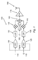
- Figure 1 illustrates a conventional I/Q transmitter arrangement 100 in which digital I and Q signals 110, 115 are converted to analogue signals by respective DACs 120, 125, and filtered by respective low pass filters (LPFs) 130, 135.
- the filtered signals are up-converted by being mixed in mixers 140, 145 with signals from a local oscillator (LO) 150.
- the LO signal supplied to the mixer 140 is 0° and that supplied to the mixer 145 is at 90°.
- the up-converted signals are then summed in 160.
- the signals are then passed via a power amplifier (PA) 170, to an antenna 180 for transmission.
- PA power amplifier
- Figure 2 illustrates a conventional polar transmitter arrangement 200 in which real and imaginary components 210, 215 are transformed from Cartesian or rectangular to polar in a converter 220.
- Outputs 230, 235 from the converter 220 correspond to amplitude and phase respectively.
- the outputs 230, 235 are converted to analogue signals in DACs 240, 245 before being filtered by LPFs 250, 255.
- the filtered signals are passed to respective amplitude and phase modulators 260, 265 before passing to a PA 270.
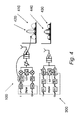
- a DDRM transmitter arrangement 300 is shown in which I and Q signals 310, 315 are digitally upsampled in 360, 365 and low-pass filtered in digital LPFs 320, 325 before being passed to digital-to-RF converters (DDRMs) 330, 335 where the signals are mixed with LO signals from a LO 340 as shown.
- the RF signals are summed and passed to PA 350, before being passed to antenna 370 for transmission.
- the filtering takes place in the digital domain prior to the direct conversion to RF.
- the DDRM transmitter arrangement 300 provides more bandwidth flexibility and has lower power consumption than the conventional polar transmitter arrangement 200. This provides a higher bandwidth before the signals are recombined in amplitude and phase. In particular, the DDRM arrangement provides easier digital modulation, better scalability, higher RF bandwidth potential, and lower area, with no synchronisation issues. However, the DDRM arrangement 300 is not as good when considering quantisation noise and DAC aliases. Efficiency is reduced by the IQ recombination. These disadvantages are due to the absence of an analogue LPF that suppresses the DAC aliases and the out-of-band quantisation noise, and the I/Q combination that adversely affects efficiency. This is illustrated in Figure 4 .
- the LPFs 130, 135 provide filtering of the aliases and the quantisation noise as shown by the graph 410.
- the RF signal after up-conversion is shown at 420.
- the aliases and the quantisation noise are also up-converted as shown with the RF signal being shown at 440.
- Graphs 410 and 430 are not shown on the same scale and the height of the respective RF signals 420 and 440 shown effectively are the same.
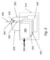
- a modulated digital input signal 500 is input to a modulator 510 that comprises a plurality of modulator elements 520, 530, 540, 550.
- the modulated digital input signal 500 may comprise a data or byte stream.
- Each modulator element 520, 530, 540, 550 comprises a mixer and PA (not shown), the current output 525, 535, 545, 555 from each modulator element 520, 530, 540, 550 being summed in a summer 560 to provide an analogue output current 565.
- Digital modulation is applied by employing a varying number of modulation elements 520, 530, 540, 550 depending on the value of input signal 500.
- any suitable number of modulator elements can be provided, for example, 2 N -1 modulator elements, in accordance with the resolution of the digital signals. For example, in one embodiment where a resolution of 8 bits is used, there may be 127 modulator elements. It is to be noted, however, that the chosen resolution may provide a compromise between performance and complexity as the number of digital levels, that is, the resolution, is related to complexity. In addition, there are other ways of determining the number of modulator elements and the above example is given by way of example only.
- a FIR DDRM can be used to overcome the problems associated with DAC aliases and quantisation noise in the receiver band
- different mixer and current control options may be provided. For example, low power may be generated and an external PA used to boost the power for transmission. By including the PA in an integrated transmitter, efficiency needs to be increased and this is done by using the switching behaviour of the LO signal so that the PA has either Class B or Class C switching.
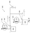
- a DDRM transmitter arrangement 700 is shown in Figure 6 .
- a modulator 710 comprises a plurality of modulator elements 720, 722, 724, 726, 728. Although five modulator elements are shown, there may be any number of modulator elements. In one embodiment, there may be 2 N -1 modulator elements as described with reference to Figure 5 above.
- Upper transistor 730 comprises a thick-gate MOSFET which is used to control the output current using a current mirror.
- Lower transistors 740, 750 comprise switches where transistor 720 is an RF switch, and transistor 730 provides an enable signal.
- a reference current 760 is provided to control the gain of the element through transistor 730.
- transistor 730 acts as a bias control.
- Shorted harmonics filter 770 comprising an inductor 774 and a capacitor 778 are provided.
- a DC blocking capacitor 780 is provided together with a load 790.
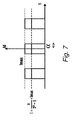
- the transmitter arrangement 700 produces a drain current as shown in Figure 7 .
- Figure 7 the effect of changing the conduction angle on efficiency is also shown.
- I max 2 N - 1 * I cell
- I n * I cell
- I dc ⁇ * I max ⁇
- I 1 2 * I max * sin ⁇ ⁇
- the shorted harmonics 770 absorb all the harmonics, the fundamental current component ( I 1 ) goes to the load.
- P out V dc * sin ⁇ * I max ⁇
- P dc V dc * ⁇ * I max ⁇
- eff max sin ⁇ ⁇
- Equation (8) shows that if the conduction angle ( ⁇ ) is zero, the maximum efficiency will be 100%, while the output power will be zero as shown in equation (6). A value needs to be chosen for ⁇ that provides a compromise between efficiency and output power. On the other hand, we should test the linearity of this transmitter.
- FIG 8 illustrates the efficiency problem in terms of I and Q components.
- a I/Q transmitter arrangement 900 includes an in-phase amplifier 910 and a quadrature amplifier 915 connected to a load 920 via DC blocking capacitors 930, 935. Harmonics shorting filters 940, 945 are also provided as shown.
- I in-phase
- Q quadrature-phase
- the optimum load impedance of the I current is changed by the Q current as imaginary components are introduced.
- the Q current is changed by the I current. This results in a reduced efficiency during modulation.
- modifying the transmitter modulator element to contain four RF phases with 25% duty cycle, a more efficient cell is provided in accordance with the present invention, as shown in Figure 9 . Such a modulator element improves efficiency as it switches between Class-B and Class-C.
- a DDRM transmitter arrangement 1000 is shown.
- a modulator 1010 is shown that comprises a plurality of modulator elements 1012, 1014, 1016, 1018. Again, although only four modulator elements are shown, there may be any number of modulator elements, for example 2 N -1 modulator elements.
- Shorted harmonics filter 1020 and a DC blocking capacitor 1030 are also provided, the capacitor 1030 being connected in series with a load 1040.
- Each modulator element 1012, 1014, 1016, 1018 comprises a common thick oxide bias transistor 1050, that controls the gain of the modulator element and protects low voltage switches formed by eight active transistors.
- the eight switches comprise four RF switches RF0, RF90, RF180, RF270, and four IQ digitally modulating enable switches EN0, EN90, E180, EN270, an RF switch and an IQ digitally modulating enable switch being required for each phase.
- Gain which determines the coefficients of the FIR function is controlled through a current mirror.
- the RF signals are designed to be 90° apart from one another with a 25% duty cycle.
- EN180 and EN270 are switched off for all modulator elements.
- EN0 and EN90 of the cells are switched with respect to the transmitted code in the first quadrant.
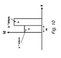
- EN0 for 'a' elements and EN90 for 'b' elements are switched on. If ' N ' represents the number of modulator elements, EN0 for 'N-a' modulator elements and EN90 for 'N-b' modulator elements are switched off. Therefore the current drain is as shown in Figure 10 .
- the DDRM topology is therefore able to perform modulation in all quadrants with relatively high efficiency and high output power.
- the drain current waveform for first quadrant modulation is shown in Figure 10 , but it will be appreciated that each quadrant is similar. If a is the number of on cells for the first phase, and b is the number of on cells for the second phase, a max is obtained when all the available cells are in an ON state. Similarly, b max , is obtained when all available cells are in an ON state.
- the element current is I e / em
- R L(optimum) ⁇ * V dc 2 * N * I elem
- a FIR DDRM transmitter 1300 in accordance with the present invention is shown in Figure 12 .
- Digital I and Q signals 1310, 1315 are up-sampled in up-samplers 1320, 1325.
- the up-sampled signals 1330, 1335 form respective inputs to amplifier 1340, 1345.
- Signals 1330, 1335 are also supplied to an amplifier 1350, 1355 via delaying flip-flops 1360, 1365.
- LO signals 1370, 1375 are provided to the amplifiers 1340, 1345, 1350, 1355 as well.
- the outputs from the amplifiers 1340, 1350 are summed in summer 1380 for the I phase and outputs from amplifiers 1345, 1355 are summed in summer 1385 for the Q phase.
- the outputs from the summers 1380, 1385 are summed in a summer 1390 before being passed to an antenna 1395 for transmission.
- the amplifiers 1340, 1345, 1350, 1355 correspond to two I/Q modulation DDRMs and the flip-flops 1360, 1365 form delays for subsequent DDRMs within the respective ones of the I and Q branch. In particular, for each extra DDRMs, an extra delaying flip flop will be necessary. Although only two DDRMs are shown, it will be appreciated that any number of DDRMs may be provided in accordance with the desired FIR filter shape with extra delaying flip flops being added as required.
- a digital signal processor (DSP) 1410 produces a signal that is input to a plurality of DDRMs 1420, 1430, 1440, 1450.
- the signal is input directly into the first DDRM 1420 and via delay units 1435, 1445, 1455 to respective ones of the subsequent DDRMs 1430, 1440, 1450.
- Each DDRM 1420, 1430, 1440, 1450 has a different gain value, a1, a2, a3, a4.
- the output from each DDRM 1420, 1430, 1440, 1450 is summed (not shown) and applied to a load 1460 via DC blocking capacitor 1470.
- Shorted harmonics filter 1480 is also included.
- DDRMs Although four DDRMs are shown and described with reference to Figure 12 , it will be appreciated at least two DDRMs are required but any suitable number may be implemented.
- FIR transmitter spectra for delay values of z -1 and z -0.5 are shown in Figures 14 and 15 for a baseband signal at 20MHz modulated on a carrier frequency of 2GHz.
- the transmitter signal 1510 is shown together with aliases 1520, 1530.
- the quantisation noise is shaped as shown at 1540.
- the transmitter signal 1610 is shown with reduced aliases 1620 and quantisation noise shaping 1630.
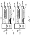
- a prototype transmitter circuit 1700 is shown in Figure 16 .
- the transmitter circuit 1700 operates on a carrier frequency of 1 GHz with a digital baseband data rate (sampling frequency) of 100MHz.
- An input data sampling frequency of 100MHz is used together with a fourth-order FIR filter.
- the maximum output power is 15dBm.
- a RF supply voltage of 2.4V is provided for the RF side together with a power supply of 1.2V for the remaining circuit.
- the transmitter circuit 1700 comprises a FIR DDRM transmitter, a RF four-phase generator and a digital circuit to transform the digital input data into suitable enable signals.
- four transmitter elements 1710, 1720, 1730, 1740 are shown connected to respective ones of a four phase input RF signals (not shown) and provide an RF output signal 1750 via a DC blocking capacitor 1755.
- Shorted harmonics filter 1760 is also provided as described above, and is connected between RF output 1750 and RF power supply 1770.
- Each transmitter element 1710, 1720, 1730, 1740 is associated with a respective delay unit 1715, 1725, 1735, 1745. Enable signals are applied to each delay unit 1715, 1725, 1735, 1745. In addition, enable signals for each transmitter element 1710, 1720, 1730, 1740 and clock signals are also provided to each delay unit 1715, 1725, 1735, 1745. Modulator element currents, I elem , are applied to each DDRM 1710, 1720, 1730, 1740 in accordance with FIR coefficients.
- Each delay unit 1715, 1725, 1735, 1745 is implemented as shown by 1780 and comprises an AND gate, a delay flip-flop and a buffer.
- the two inputs to the AND gate comprise the enable signal and the transmitter enable signal.
- Each DDRM 1710, 1720, 1730, 1740 comprises multiple modulator elements 1790 as described above with reference to Figure 9 .
- the circuit 1700 comprises four DDRMs.
- Each DDRM or transmitter element 1710, 1720, 1730, 1740 comprises 127 modulator elements (2 7 -1).
- upper transistor is a thick-gate transistor used to control the current of each transistor element, and hence to control the output power, and the FIR coefficients. It is chosen as a thick gate to increase the supply voltage to be 2.4V instead 1.2V, and hence quadrupling the maximum output power.
- the enable signals making the digital modulation are delayed by four banks of delay units 1715, 1725, 1735, 1745.
- Each delay unit contains AND gate to enable or disable the transmitter element, and a buffer to be able to switch subsequent transistor elements.
- V bias signals are provided, one for the middle FIR coefficients and another for the outer FIR coefficients.
- the FIR coefficients and the position of the filter notch can be adjusted so that the notch corresponds with the frequency band with the toughest noise requirements. This will mostly be the received band related to the transmit frequency.
- two RF signals having 180° phase difference with 50% duty cycle form input signals for frequency division to generate four phases RF signals with 25% duty cycle.
- the RF signals are 2GHz square waves at 50% duty cycle with four output RF signals in quadrature as 1 GHz square waves at 25% duty cycle.
- the four RF signals are buffered to drive the load capacitance. This load capacitance is the sum of parasitic capacitances of the RF switches of the FIR transmitter elements.
- Digital decoding is used to decode the 16-bit input digital data to provide suitable enable signals for the FIR transmitter element to perform the digital modulation.
- the 16 bits consist of 8 bits for the real input part (I) and 8 bits for the imaginary input part (Q).
- This is shown in decoding circuit 1800 shown in Figure 17 .
- Two 8-bit words 1810, 1815 are provided one for the real part and one for the imaginary part. These two words 1810, 1815 are applied to respective positive-negative splitters 1820, 1825 which generates two 7-bit words that control the digital modulation of the circuit.
- MSBs most significant bits
- the other 3 bits directly control binary scaled sections of the modulator. This gives a good compromise between circuit complexity and Differential non-linearity (DNL) and integral non-linearity (INL) of the DDRM.
- DNL Differential non-linearity
- INL integral non-linearity
- Each binary-to-thermometer decoding block 1830, 1835, 1840, 1845 provides an output that corresponds to MSBs as shown. Only four MSBs are processed in the binary-to-thermometer decoding blocks 1830, 1835, 1840, 1845 to reduce connection complexity. Buffers (not shown) may be used after the decoding due to the long wiring to the FIR transmitter elements (not shown).
- Each positive-negative splitter 1820, 1825 uses the MSB to determine the polarity of the current which is to be applied to the load, while the other bits are used to perform the digital modulation.
- Figure 18 illustrates a possible chip layout 1900 for a DDRM with FIR notch filter arrangement in accordance with the present invention. Elements in the layout are arranged so that the distribution of the RF signals avoids delay inconsistencies, and the distance between different RF input signals is such that cross-talk is reduced.
- the layout 1900 comprises a digital decoding unit 1910, four transmitter elements 1920, 1930, 1940, 1950, an RF 4-phase generator 1960 for generating a phase for each transmitter element 1920, 1930, 1940, 1950, current mirrors 1970 and an RF-choke tuning tank 1980.
- Input signals in-phase and quadrature signals 1904, 1908 are applied to the digital decoding unit 1910.
- Decoded signal 1915 is transmitted to transmitter elements 1920, 1930, 1940, 1950 in turn as shown.
- RF output signal 1985 is provided by RF-choke tuning tank 1980 as shown.
- a multi-phase generator may also be used depending on the number of modulator elements provided.
- the generator may be implemented by a multi-phase switch that switches in multiples of four, namely, four, eight etc.
- the RF input lines to the transmitter elements 1920, 1930, 1940, 1950 are tree shaped.
- the lateral distance between the transmitter elements 1920, 1930, 1940, 1950 is reduced by placing the RF 4-phase generator 1960 in the middle to prevent RF lines from passing between transmitter element 1920 and transmitter element 1950 or between transmitter element 1930 and transmitter element 1940.
- RF output signal 1985 is located so to avoid any high series parasitic resistance that can reduce the efficiency of each transmitter element 1920, 1930, 1940, 1950.
- Supply line, output line and ground line connections have low impedances and carry the large signal currents.
- Ground connections are made by four different bond pads to reduce the parasitic resistance and the inductance of the ground connection which absorb a lot of current.
- the RF output 1985 is arranged to be orthogonal to RF inputs to the RF generator 1960. This is to avoid any coupling between the inputs and the output.
- thermometer bits increase the circuit complexity, a balance needs to be made between the performance and complexity.
- the four MSBs are transformed into thermometer (16-bits) and the three LSBs remain the same.
- Output buffers are provided by large transistors, due to the high load capacitance (all the modulation elements of the four transmitters). For a supply voltage of 1.2V, the ground connections need to be wide enough to carry this current. Further, there are two VDD bond pads to facilitate the flow of current. The power consumption of this circuit is critical, since it consumes a lot of power which reduces the overall system efficiency.
- the maximum power of the circuit is 15dBm (31.6mW), and the 2.4V supply gives 21dBm (125mW) consumption power, so the drain efficiency is 25%.
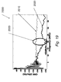
- a measured spectrum 2000 obtained from the prototype transmitter is shown in Figure 19 .
- a noise floor comparison at 900MHz carrier frequency and 75MHz sampling frequency is shown together with a 200kHz baseband tone at maximum power, that is, -152dBc/Hz at 20MHz.
- Trace 2010 indicates the noise floor without FIR and trace 2020 indicates the noise floor with FIR in accordance with the present invention.
- the quantisation noise is clearly reduced at 20MHz offset, while the notch created by the FIR function is also clearly visible as indicated by 2030.
Landscapes
- Engineering & Computer Science (AREA)
- Theoretical Computer Science (AREA)
- Computer Networks & Wireless Communication (AREA)
- Signal Processing (AREA)
- Transmitters (AREA)
Priority Applications (1)
| Application Number | Priority Date | Filing Date | Title |
|---|---|---|---|
| EP11171905A EP2541776A1 (de) | 2011-06-29 | 2011-06-29 | Funkfrequenzmodulatoren |
Applications Claiming Priority (1)
| Application Number | Priority Date | Filing Date | Title |
|---|---|---|---|
| EP11171905A EP2541776A1 (de) | 2011-06-29 | 2011-06-29 | Funkfrequenzmodulatoren |
Publications (1)
| Publication Number | Publication Date |
|---|---|
| EP2541776A1 true EP2541776A1 (de) | 2013-01-02 |
Family
ID=45446273
Family Applications (1)
| Application Number | Title | Priority Date | Filing Date |
|---|---|---|---|
| EP11171905A Withdrawn EP2541776A1 (de) | 2011-06-29 | 2011-06-29 | Funkfrequenzmodulatoren |
Country Status (1)
| Country | Link |
|---|---|
| EP (1) | EP2541776A1 (de) |
Cited By (1)
| Publication number | Priority date | Publication date | Assignee | Title |
|---|---|---|---|---|
| US20230090369A1 (en) * | 2021-09-23 | 2023-03-23 | Noam Familia | Apparatus and method for clock phase calibration |
Citations (3)
| Publication number | Priority date | Publication date | Assignee | Title |
|---|---|---|---|---|
| WO2006117590A1 (en) * | 2005-04-29 | 2006-11-09 | Nokia Corporation | Polar transmitter with digital to rf converter |
| EP2037584A1 (de) * | 2007-09-14 | 2009-03-18 | STMicroelectronics N.V. | Verfahren zur Durchführung einer Digital-Analog-Wandlung eines digitalen Signals und entsprechende elektronische Vorrichtung |
| US7528754B1 (en) | 2006-02-09 | 2009-05-05 | Arizona Board Of Regents | Finite impulse response digital to analog converter |
-
2011
- 2011-06-29 EP EP11171905A patent/EP2541776A1/de not_active Withdrawn
Patent Citations (3)
| Publication number | Priority date | Publication date | Assignee | Title |
|---|---|---|---|---|
| WO2006117590A1 (en) * | 2005-04-29 | 2006-11-09 | Nokia Corporation | Polar transmitter with digital to rf converter |
| US7528754B1 (en) | 2006-02-09 | 2009-05-05 | Arizona Board Of Regents | Finite impulse response digital to analog converter |
| EP2037584A1 (de) * | 2007-09-14 | 2009-03-18 | STMicroelectronics N.V. | Verfahren zur Durchführung einer Digital-Analog-Wandlung eines digitalen Signals und entsprechende elektronische Vorrichtung |
Non-Patent Citations (2)
| Title |
|---|
| SHAHIN MEHDIZAD TALEIE ET AL: "A Linear â Digital IF to RF DAC Transmitter With Embedded Mixer", IEEE TRANSACTIONS ON MICROWAVE THEORY AND TECHNIQUES, IEEE SERVICE CENTER, PISCATAWAY, NJ, US, vol. 55, no. 5, 1 May 2008 (2008-05-01), pages 1059 - 1068, XP011206782, ISSN: 0018-9480 * |
| TALEIE S M ET AL: "A Bandpass /spl Delta//spl Sigma/ RF-DAC with Embedded FIR Reconstruction Filter", DIGEST OF TECHNICAL PAPERS / 2006 IEEE INTERNATIONAL SOLID-STATE CIRCUITS CONFERENCE : SAN FRANCISCO, CA, 5 - 9 FEBRUARY 2006, IEEE SERVICE CENTER, PISCATAWAY, NJ , US, 6 February 2006 (2006-02-06), pages 2370 - 2379, XP010940644, ISBN: 978-1-4244-0079-9, DOI: 10.1109/ISSCC.2006.1696300 * |
Cited By (2)
| Publication number | Priority date | Publication date | Assignee | Title |
|---|---|---|---|---|
| US20230090369A1 (en) * | 2021-09-23 | 2023-03-23 | Noam Familia | Apparatus and method for clock phase calibration |
| US12381706B2 (en) * | 2021-09-23 | 2025-08-05 | Intel Corporation | Apparatus and method for clock phase calibration |
Similar Documents
| Publication | Publication Date | Title |
|---|---|---|
| CN106471734B (zh) | 开关电容器发射器电路及方法 | |
| US7729445B2 (en) | Digital outphasing transmitter architecture | |
| US9088319B2 (en) | RF transmitter architecture, integrated circuit device, wireless communication unit and method therefor | |
| Ye et al. | A digitally modulated 2.4 GHz WLAN transmitter with integrated phase path and dynamic load modulation in 65nm CMOS | |
| TWI571061B (zh) | 多波段產生系統及方法 | |
| US10644656B2 (en) | RF-DAC based phase modulator | |
| US9647866B2 (en) | RF transmitter, integrated circuit device, wireless communication unit and method therefor | |
| US9813086B2 (en) | RF transmitter, integrated circuit device, wireless communication unit and method therefor | |
| JP2012060645A (ja) | 無線送信機 | |
| US9071204B2 (en) | Digital polar and ZVS contour based hybrid power amplifier | |
| EP2515444A1 (de) | HF-Sender und Verfahren dafür | |
| WO2006051349A1 (en) | Rf transmitter using digital-to-rf conversion | |
| US20130003881A1 (en) | Radio Frequency Modulators | |
| Zheng et al. | A 6-GHz MU-MIMO eight-element direct digital beamforming TX utilizing FIR H-bridge DAC | |
| US6690313B1 (en) | Digital-to-analog upconverter | |
| Dinis et al. | An FPGA-based multi-level all-digital transmitter with 1.25 GHz of bandwidth | |
| Zheng et al. | A two-beam eight-element direct digital beamforming RF modulator in 40-nm CMOS | |
| Zheng et al. | A 6 GHz 160 MHz bandwidth MU-MIMO eight-element direct digital beamforming TX utilizing FIR H-bridge DAC | |
| EP2541776A1 (de) | Funkfrequenzmodulatoren | |
| CN103888155B (zh) | 射频发射机、集成电路器件、无线通信单元及相关方法 | |
| Zimmermann | Design and implementation of a broadband RF-DAC transmitter for wireless communications | |
| KR101292667B1 (ko) | 디지털 rf 컨버터 및 이를 포함하는 디지털 rf 변조기와 송신기 | |
| Mehboob et al. | A novel IFPWM‐based all‐digital transmitter architecture and FPGA implementation | |
| LaRue | A Fully-Integrated Four-way Outphasing Architecture in Heterogeneously Integrated CMOS/GaN Process Technologies | |
| Seddighrad | Digitally-scalable transformer-combining power amplifier techniques |
Legal Events
| Date | Code | Title | Description |
|---|---|---|---|
| PUAI | Public reference made under article 153(3) epc to a published international application that has entered the european phase |
Free format text: ORIGINAL CODE: 0009012 |
|
| AK | Designated contracting states |
Kind code of ref document: A1 Designated state(s): AL AT BE BG CH CY CZ DE DK EE ES FI FR GB GR HR HU IE IS IT LI LT LU LV MC MK MT NL NO PL PT RO RS SE SI SK SM TR |
|
| AX | Request for extension of the european patent |
Extension state: BA ME |
|
| 17P | Request for examination filed |
Effective date: 20130516 |
|
| 17Q | First examination report despatched |
Effective date: 20131008 |
|
| STAA | Information on the status of an ep patent application or granted ep patent |
Free format text: STATUS: THE APPLICATION IS DEEMED TO BE WITHDRAWN |
|
| 18D | Application deemed to be withdrawn |
Effective date: 20150421 |