EP2544240A1 - Halbleiter-transistor - Google Patents
Halbleiter-transistor Download PDFInfo
- Publication number
- EP2544240A1 EP2544240A1 EP11750724A EP11750724A EP2544240A1 EP 2544240 A1 EP2544240 A1 EP 2544240A1 EP 11750724 A EP11750724 A EP 11750724A EP 11750724 A EP11750724 A EP 11750724A EP 2544240 A1 EP2544240 A1 EP 2544240A1
- Authority
- EP
- European Patent Office
- Prior art keywords
- insulating film
- gan
- gate insulating
- film
- semiconductor transistor
- Prior art date
- Legal status (The legal status is an assumption and is not a legal conclusion. Google has not performed a legal analysis and makes no representation as to the accuracy of the status listed.)
- Granted
Links
Images

Classifications
-
- H—ELECTRICITY
- H10—SEMICONDUCTOR DEVICES; ELECTRIC SOLID-STATE DEVICES NOT OTHERWISE PROVIDED FOR
- H10D—INORGANIC ELECTRIC SEMICONDUCTOR DEVICES
- H10D64/00—Electrodes of devices having potential barriers
- H10D64/01—Manufacture or treatment
- H10D64/013—Manufacture or treatment of electrodes having a conductor capacitively coupled to a semiconductor by an insulator
- H10D64/01358—Manufacture or treatment of electrodes having a conductor capacitively coupled to a semiconductor by an insulator the insulator being formed after the semiconductor body, the semiconductor being a Group III-V material
-
- C—CHEMISTRY; METALLURGY
- C23—COATING METALLIC MATERIAL; COATING MATERIAL WITH METALLIC MATERIAL; CHEMICAL SURFACE TREATMENT; DIFFUSION TREATMENT OF METALLIC MATERIAL; COATING BY VACUUM EVAPORATION, BY SPUTTERING, BY ION IMPLANTATION OR BY CHEMICAL VAPOUR DEPOSITION, IN GENERAL; INHIBITING CORROSION OF METALLIC MATERIAL OR INCRUSTATION IN GENERAL
- C23C—COATING METALLIC MATERIAL; COATING MATERIAL WITH METALLIC MATERIAL; SURFACE TREATMENT OF METALLIC MATERIAL BY DIFFUSION INTO THE SURFACE, BY CHEMICAL CONVERSION OR SUBSTITUTION; COATING BY VACUUM EVAPORATION, BY SPUTTERING, BY ION IMPLANTATION OR BY CHEMICAL VAPOUR DEPOSITION, IN GENERAL
- C23C16/00—Chemical coating by decomposition of gaseous compounds, without leaving reaction products of surface material in the coating, i.e. chemical vapour deposition [CVD] processes
- C23C16/22—Chemical coating by decomposition of gaseous compounds, without leaving reaction products of surface material in the coating, i.e. chemical vapour deposition [CVD] processes characterised by the deposition of inorganic material, other than metallic material
- C23C16/30—Deposition of compounds, mixtures or solid solutions, e.g. borides, carbides, nitrides
- C23C16/40—Oxides
- C23C16/403—Oxides of aluminium, magnesium or beryllium
-
- C—CHEMISTRY; METALLURGY
- C23—COATING METALLIC MATERIAL; COATING MATERIAL WITH METALLIC MATERIAL; CHEMICAL SURFACE TREATMENT; DIFFUSION TREATMENT OF METALLIC MATERIAL; COATING BY VACUUM EVAPORATION, BY SPUTTERING, BY ION IMPLANTATION OR BY CHEMICAL VAPOUR DEPOSITION, IN GENERAL; INHIBITING CORROSION OF METALLIC MATERIAL OR INCRUSTATION IN GENERAL
- C23C—COATING METALLIC MATERIAL; COATING MATERIAL WITH METALLIC MATERIAL; SURFACE TREATMENT OF METALLIC MATERIAL BY DIFFUSION INTO THE SURFACE, BY CHEMICAL CONVERSION OR SUBSTITUTION; COATING BY VACUUM EVAPORATION, BY SPUTTERING, BY ION IMPLANTATION OR BY CHEMICAL VAPOUR DEPOSITION, IN GENERAL
- C23C16/00—Chemical coating by decomposition of gaseous compounds, without leaving reaction products of surface material in the coating, i.e. chemical vapour deposition [CVD] processes
- C23C16/44—Chemical coating by decomposition of gaseous compounds, without leaving reaction products of surface material in the coating, i.e. chemical vapour deposition [CVD] processes characterised by the method of coating
- C23C16/448—Chemical coating by decomposition of gaseous compounds, without leaving reaction products of surface material in the coating, i.e. chemical vapour deposition [CVD] processes characterised by the method of coating characterised by the method used for generating reactive gas streams, e.g. by evaporation or sublimation of precursor materials
- C23C16/4488—Chemical coating by decomposition of gaseous compounds, without leaving reaction products of surface material in the coating, i.e. chemical vapour deposition [CVD] processes characterised by the method of coating characterised by the method used for generating reactive gas streams, e.g. by evaporation or sublimation of precursor materials by in situ generation of reactive gas by chemical or electrochemical reaction
-
- H—ELECTRICITY
- H10—SEMICONDUCTOR DEVICES; ELECTRIC SOLID-STATE DEVICES NOT OTHERWISE PROVIDED FOR
- H10D—INORGANIC ELECTRIC SEMICONDUCTOR DEVICES
- H10D30/00—Field-effect transistors [FET]
- H10D30/60—Insulated-gate field-effect transistors [IGFET]
-
- H—ELECTRICITY
- H10—SEMICONDUCTOR DEVICES; ELECTRIC SOLID-STATE DEVICES NOT OTHERWISE PROVIDED FOR
- H10D—INORGANIC ELECTRIC SEMICONDUCTOR DEVICES
- H10D64/00—Electrodes of devices having potential barriers
- H10D64/60—Electrodes characterised by their materials
- H10D64/66—Electrodes having a conductor capacitively coupled to a semiconductor by an insulator, e.g. MIS electrodes
- H10D64/68—Electrodes having a conductor capacitively coupled to a semiconductor by an insulator, e.g. MIS electrodes characterised by the insulator, e.g. by the gate insulator
- H10D64/681—Electrodes having a conductor capacitively coupled to a semiconductor by an insulator, e.g. MIS electrodes characterised by the insulator, e.g. by the gate insulator having a compositional variation, e.g. multilayered
- H10D64/685—Electrodes having a conductor capacitively coupled to a semiconductor by an insulator, e.g. MIS electrodes characterised by the insulator, e.g. by the gate insulator having a compositional variation, e.g. multilayered being perpendicular to the channel plane
-
- H—ELECTRICITY
- H10—SEMICONDUCTOR DEVICES; ELECTRIC SOLID-STATE DEVICES NOT OTHERWISE PROVIDED FOR
- H10D—INORGANIC ELECTRIC SEMICONDUCTOR DEVICES
- H10D64/00—Electrodes of devices having potential barriers
- H10D64/60—Electrodes characterised by their materials
- H10D64/66—Electrodes having a conductor capacitively coupled to a semiconductor by an insulator, e.g. MIS electrodes
- H10D64/68—Electrodes having a conductor capacitively coupled to a semiconductor by an insulator, e.g. MIS electrodes characterised by the insulator, e.g. by the gate insulator
- H10D64/691—Electrodes having a conductor capacitively coupled to a semiconductor by an insulator, e.g. MIS electrodes characterised by the insulator, e.g. by the gate insulator comprising metallic compounds, e.g. metal oxides or metal silicates
-
- H—ELECTRICITY
- H10—SEMICONDUCTOR DEVICES; ELECTRIC SOLID-STATE DEVICES NOT OTHERWISE PROVIDED FOR
- H10P—GENERIC PROCESSES OR APPARATUS FOR THE MANUFACTURE OR TREATMENT OF DEVICES COVERED BY CLASS H10
- H10P14/00—Formation of materials, e.g. in the shape of layers or pillars
- H10P14/60—Formation of materials, e.g. in the shape of layers or pillars of insulating materials
- H10P14/63—Formation of materials, e.g. in the shape of layers or pillars of insulating materials characterised by the formation processes
- H10P14/6326—Deposition processes
- H10P14/6328—Deposition from the gas or vapour phase
- H10P14/6334—Deposition from the gas or vapour phase using decomposition or reaction of gaseous or vapour phase compounds, i.e. chemical vapour deposition
- H10P14/6338—Deposition from the gas or vapour phase using decomposition or reaction of gaseous or vapour phase compounds, i.e. chemical vapour deposition the reactions being activated by other means than plasma or thermal, e.g. photo-CVD
-
- H—ELECTRICITY
- H10—SEMICONDUCTOR DEVICES; ELECTRIC SOLID-STATE DEVICES NOT OTHERWISE PROVIDED FOR
- H10P—GENERIC PROCESSES OR APPARATUS FOR THE MANUFACTURE OR TREATMENT OF DEVICES COVERED BY CLASS H10
- H10P14/00—Formation of materials, e.g. in the shape of layers or pillars
- H10P14/60—Formation of materials, e.g. in the shape of layers or pillars of insulating materials
- H10P14/69—Inorganic materials
- H10P14/692—Inorganic materials composed of oxides, glassy oxides or oxide-based glasses
- H10P14/6938—Inorganic materials composed of oxides, glassy oxides or oxide-based glasses the material containing at least one metal element, e.g. metal oxides, metal oxynitrides or metal oxycarbides
- H10P14/6939—Inorganic materials composed of oxides, glassy oxides or oxide-based glasses the material containing at least one metal element, e.g. metal oxides, metal oxynitrides or metal oxycarbides characterised by the metal
- H10P14/69391—Inorganic materials composed of oxides, glassy oxides or oxide-based glasses the material containing at least one metal element, e.g. metal oxides, metal oxynitrides or metal oxycarbides characterised by the metal the material containing aluminium, e.g. Al2O3
-
- H—ELECTRICITY
- H10—SEMICONDUCTOR DEVICES; ELECTRIC SOLID-STATE DEVICES NOT OTHERWISE PROVIDED FOR
- H10D—INORGANIC ELECTRIC SEMICONDUCTOR DEVICES
- H10D62/00—Semiconductor bodies, or regions thereof, of devices having potential barriers
- H10D62/80—Semiconductor bodies, or regions thereof, of devices having potential barriers characterised by the materials
- H10D62/85—Semiconductor bodies, or regions thereof, of devices having potential barriers characterised by the materials being Group III-V materials, e.g. GaAs
- H10D62/8503—Nitride Group III-V materials, e.g. AlN or GaN
Definitions
- the present invention relates to a semiconductor transistor, and more particularly to a semiconductor transistor having an active layer made of a GaN-based semiconductor.
- a gallium nitride-based semiconductor transistor (hereinafter, referred to as a GaN-based semiconductor transistor) has, for example, an active layer composed of a GaN-based semiconductor and a gate insulating film formed on the active layer.
- the gate insulating film for example, SiO 2 , Al 2 O 3 , SiNx, GaOx, or HfO 2 is used.
- JP-A Japanese Patent Application Laid-Open
- JP-A No. 2008-277640 can prevent the Si of the SiO 2 from diffusing into the GaN.
- a gate insulating film composed of Al 2 O 3 has poorer film characteristics than a gate insulating film composed of SiO 2 .
- the poorer film characteristics mean, for example, that leaked electric current is high, breakdown voltage is low, and the like.
- the present inventors have found that when SiO 2 is used for a gate insulating film in a GaN-based semiconductor transistor, there occurs a mutual diffusion phenomenon in which not only does the Si of the SiO 2 diffuse into the GaN, but also, conversely, an impurity diffuses from the GaN into the SiO 2 .
- the mutual diffusion phenomenon occurs, the interface state increases, and the interface characteristics between the GaN-based semiconductor and the gate insulating film deteriorate.
- the present inventors have found that the mutual diffusion phenomenon is attributable to the oxidization power of a compound that forms a gate insulating film.
- the present inventors have also found that it is not enough for the compound that forms the gate insulating film to merely have a wider Eg (band gap) than the GaN that forms the active layer, and that the presence of ⁇ Ec (a conduction band barrier) and ⁇ Ev (a valence band barrier) is necessary.
- a GaN-based semiconductor is one kind of so-called wide band gap semiconductors and is expected to be used in a high temperature environment.
- examples of the compound that forms the gate insulating film of the GaN-based semiconductor transistor include SiO 2 and Al 2 O 3 , which have a wider band gap than the GaN-based semiconductor and have good high-temperature characteristics.
- Al 2 O 3 has a stronger oxidization power than SiO 2 . Therefore, formation of a gate insulating film from Al 2 O 3 prevents, for example, diffusion of impurity from the GaN-based semiconductor into the Al 2 O 3 , thereby improving interface characteristics, even in a high temperature environment. However, it is difficult to provide an Al 2 O 3 with excellent film quality.
- SiO 2 has a wider band gap than Al 2 O 3 and thus the breakdown voltage is high and the film quality is good.
- SiO 2 exhibits lower oxidization power than Al 2 O 3 , due to impurity diffusion or the like, interface characteristics are not favorable. Therefore, in GaN-based semiconductor transistors, even with the use of SiO 2 or Al 2 O 3 for a gate insulating film, it has been difficult to improve both the interface characteristics between the GaN-based semiconductor and the gate insulating film and the film characteristics of the gate insulating film.
- JP-A No. 2008-103408 describes a GaN-based semiconductor transistor in which a first gate insulating film composed of SiNx is formed on a GaN-based semiconductor, and a second gate insulating film composed of Al 2 O 3 or SiO 2 , which have greater breakdown strength than SiNx, is formed on the first gate insulating film.
- the gate insulating film is formed as a composite film (hybrid film), with the intention of providing favorable interface characteristics between a first gate insulating film in the GaN-based semiconductor and the gate insulating film and obtaining a high breakdown voltage in a second gate insulating film.
- An object of the present invention is to provide a semiconductor transistor that has both favorable interface characteristics between a GaN-based semiconductor and a gate insulating film and favorable film characteristics of the gate insulating film.
- the present invention provides a semiconductor transistor that includes an active layer composed of a GaN-based semiconductor; and a gate insulating film having a first insulating film including one or more compounds selected from the group consisting of insulating films in which an absolute value of standard enthalpy of formation is larger than 228 kJ/mol, and a second insulating film composed of SiO 2 formed on the first insulating film.
- a semiconductor transistor that includes an active layer composed of a GaN-based semiconductor; and a gate insulating film having a first insulating film including one or more compounds selected from the group consisting of Al 2 O 3 , HfO 2 , ZrO 2 , La 2 O 3 , and Y 2 O 3 , and a second insulating film composed of SiO 2 formed on the first insulating film, is also provided.
- the semiconductor transistor according to the present invention has both favorable interface characteristics between the GaN-based semiconductor and the gate insulating film and favorable film characteristics of the gate insulating film.
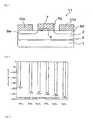
- Fig. 1 is a cross-sectional view showing a configuration of the GaN-based semiconductor transistor according to an embodiment of the invention.
- FIG. 1 is a cross-sectional view showing a configuration of a semiconductor transistor according to an embodiment of the present invention.
- a semiconductor transistor 11 is a GaN-based semiconductor transistor having an active layer composed of a GaN-based semiconductor.
- the semiconductor transistor 11 has a buffer layer 2 formed on a substrate 1, a p-type active layer (p-GaN) 3 formed on the buffer layer 2 using a group-III nitride semiconductor, and a gate insulating film composed of a first insulating film 6 and a second insulating film 7 formed on the active layer 3.
- p-GaN p-type active layer
- the semiconductor layer 11 includes a gate electrode 8g which is provided on the active layer 3 with the gate insulating film therebetween, and an n+ type source region 5s and an n+ type drain region 5d, which are provided suitably for the gate electrode 8g and are in ohmic contact with a source electrode 10s and a drain electrode 10d, respectively.
- the gate insulating film is a hybrid film composed of the first insulating film 6 and the second insulating film 7.
- the first insulating film 6 is formed on the active layer 3 and includes one or more compounds selected from the group consisting of Al 2 O 3 , HfO 2 , ZrO 2 , La 2 O 3 , and Y 2 O 3 .
- the second insulating film 7 is formed on the first insulating film 6 and is composed of SiO 2 .
- the present inventors have found that when SiO 2 is used for a gate insulating film in a GaN-based semiconductor transistor, not only does the Si of the SiO 2 diffuse into the GaN, but also, conversely, a mutual diffusion phenomenon in which an impurity diffuses from the GaN into the SiO 2 occurs, and furthermore, that the mutual diffusion phenomenon is attributable to the oxidization power of the compound that forms the gate insulating film.
- the mutual diffusion phenomenon occurs, the interface state increases, whereby the interface characteristics between the GaN-based semiconductor and the gate insulating film deteriorate. Therefore, to suppress the mutual diffusion phenomenon, it is necessary to use a compound having a higher oxidization power than SiO 2 for the gate insulating film.
- Fig. 2 shows the oxidization power of respective compounds.
- the oxidization power is represented by a standard enthalpy of formation per 1 mol of metal-oxygen bonding, which is an absolute value of a vertical axis ⁇ Hf0 [KJ/mol] in the drawing.
- the oxidization power of SiO 2 is 228; the oxidization power of ZrO 2 is 275; the oxidization power of Al 2 O 3 is 279; the oxidization power of HfO 2 is 286; the oxidization power of La 2 O 3 is 299, and the oxidization power of Y 2 O 3 is 318.
- the oxidization power of Al 2 O 3 , HfO 2 , ZrO 2 , La 2 O 3 , and Y 2 O 3 are higher than that of SiO 2 .
- the present inventors have also focused on the band structure of a compound, and consequently have found that the compound that forms the gate insulating film of the GaN-based semiconductor transistor has a wider Eg (band gap) than the GaN which forms the active layer 3, and the presence of ⁇ Ec (a conduction band barrier) and ⁇ Ev (a valence band barrier) is necessary.
- Eg band gap
- ⁇ Ec conduction band barrier
- ⁇ Ev a valence band barrier
- Fig. 3 shows the band structure of each compound.
- the Eg of each of HfO 2 and ZrO 2 is 6.0 ev; the Eg of Al 2 O 3 is 8.8 ev; the Eg of La 2 O 3 is 6.0 ev; and the Eg of Y 2 O 3 is 5.6 ev. Accordingly, it is apparent that the Eg of SiO 2 is the largest.
- the first insulating film 6 was formed with a compound having a higher oxidization power than SiO 2 to provide favorable interface characteristics between the gate insulating film and the active layer 3, and the second insulating film 7 was formed with a compound having a wider band gap than the first insulating film 6 to provide favorable film characteristics of the gate insulating film.
- the buffer layer 2 composed of AlN or GaN and having a thickness of approximately 20 nm and the p-GaN layer 3 having a thickness of approximately 1 ⁇ m are sequentially grown on the substrate 1 made of, for example, sapphire, SiC, Si, GaN or the like by a metal organic chemical vapor deposition (MOCVD) method.
- MOCVD metal organic chemical vapor deposition
- Mg is used as a p-type dopant
- the dopant concentration is, for example, set to 1 ⁇ 10 16 to 1 ⁇ 10 17 /cm 3 .
- the growth of GaN or the like on the substrate 1 is not limited to the MOCVD method, and other growth methods such as a hydride vapor phase epitaxy (HVPE) method or a molecular beam epitaxy (MBE) method may be used.
- HVPE hydride vapor phase epitaxy
- MBE molecular beam epitaxy
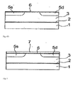
- a photoresist 4 is applied to the p-GaN layer 3 and exposed to light and developed to form openings in a source region and a drain region.
- an n-type dopant such as silicon is injected to form the n+ type source region 5s and the n+ type drain region 5d.
- the concentration of the n-type dopant is set to, for example, 1 ⁇ 10 18 to 2 ⁇ 10 20 /cm 3 .
- an alumina film (Al 2 O 3 ) that is to be the first insulating film 6 is grown so as to have a thickness of, for example, from 5 nm to 10 nm, by a plasma-free catalytic chemical vapor deposition (Cat-CVD) method.
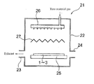
- the Cat-CVD method is performed, for example, using the film formation apparatus 21 shown in Fig. 5 .
- the film formation apparatus 21 includes a chamber 22, as shown in Fig. 5 .
- a chamber 22 In the chamber 22 an exhaust outlet 23 and a substrate-conveying opening 24 are provided.
- a substrate-mounting table 25 for mounting the substrate 1 a gas-discharging device 26, and a linear catalyst 27 are disposed inside the chamber 22 .
- the gas-discharging device 26 discharges, to the substrate-mounting table 25, a reaction (raw material) gas which has been introduced from outside.
- the catalyst 27 is composed of tungsten and is placed between the substrate-mounting table 25 and the gas-discharging device 26.
- the substrate 1 on which the p-GaN layer 3 has been formed is mounted on the substrate-mounting table 25, the pressure inside the chamber 22 is reduced, and an electric current is supplied from an alternating current source (not shown) to the catalyst 27 to achieve a state in which the temperature thereof is increased to approximately from 1800°C to 1900°C.
- a raw material gas is discharged from the gas-discharging device 26 to the p-GaN layer 3.
- the raw material gas is decomposed by the catalyzer 27 to produce an active species, whereby the alumina film (first insulating film) 6 is formed on a surface of the p-GaN layer 3.
- a silicon oxide film (SiO 2 film) that is to be the second insulating film 7 is formed, on the alumina film 6, so as to have a thickness of approximately from 50 nm to 100 nm.
- a conductive film 8 is formed on the silicon oxide film 7.
- Polysilicon is generally used for the conductive film 8, but the conductive film 8 is not restricted thereto, and may be a metal film such as Ni/Al or WSi.
- P phosphorous
- B boron
- polysilicon is grown by the CVD method, whereas, in the case of a metal film, it is formed by sputtering or the like.
- a photoresist 9 is applied to the conductive film 8, and is exposed to light and developed, as a result of which, the photoresist 9 remains in the gate region, but is removed from the source region 5s and the drain region 5d.
- etching is performed on the conductive film 8, the silicon oxide film 7, and the alumina film 6, and the conductive film 8 left on the gate region serves as the gate electrode 8g.
- the silicon oxide film 7 and the alumina film 6 under the gate electrode 8g serve as the gate insulating film.
- a source electrode 10s is formed on the source region 5s and simultaneously, a drain electrode 10d is formed on the drain region 5d, by a lift-off method using another photoresist (not shown).
- Each of the source electrode 10s and the drain electrode 10d is a film composed of, for example, Ti/Al, Ti/AlSi, Mo, or the like and is in ohmic contact with the n+-GaN layer that forms the drain region 5d and the source region 5s.
- the gate insulating film was formed as a hybrid film composed of the first insulating film 6 and the second insulating film 7, in which the first insulating film 6 was made of one or more compounds selected from the group consisting of Al 2 O 3 , HfO 2 , ZrO 2 , La 2 O 3 , and Y 2 O 3 and having a higher oxidization power than that of SiO 2 , and the second insulating film 7 was made of SiO 2 as a compound having a wider band gap than the first insulating film 6.
- the semiconductor transistor 11 has both favorable interface characteristics between the GaN-based semiconductor and the gate insulating film and favorable film characteristics of the gate insulating film.
- the semiconductor transistor 11 will be used, for example, as a power device for automobiles, home appliance power circuits, and the like, but not in an LSI of a so-called signal system.
- the semiconductor transistor 11 can be suitably used as a power device.
- the present invention has been described based on a preferable embodiment.
- the semiconductor transistor according to the present invention is not restricted simply to the configuration of this embodiment.
- Various changes and modifications in the configuration of the embodiment are also encompassed in the scope of the invention.
Landscapes
- Chemical & Material Sciences (AREA)
- General Chemical & Material Sciences (AREA)
- Engineering & Computer Science (AREA)
- Chemical Kinetics & Catalysis (AREA)
- Mechanical Engineering (AREA)
- Materials Engineering (AREA)
- Metallurgy (AREA)
- Organic Chemistry (AREA)
- Electrochemistry (AREA)
- Inorganic Chemistry (AREA)
- Insulated Gate Type Field-Effect Transistor (AREA)
- Thin Film Transistor (AREA)
- Formation Of Insulating Films (AREA)
- Physics & Mathematics (AREA)
- Plasma & Fusion (AREA)
Applications Claiming Priority (2)
| Application Number | Priority Date | Filing Date | Title |
|---|---|---|---|
| JP2010045547A JP5506036B2 (ja) | 2010-03-02 | 2010-03-02 | 半導体トランジスタ |
| PCT/JP2011/054815 WO2011108615A1 (ja) | 2010-03-02 | 2011-03-02 | 半導体トランジスタ |
Publications (3)
| Publication Number | Publication Date |
|---|---|
| EP2544240A1 true EP2544240A1 (de) | 2013-01-09 |
| EP2544240A4 EP2544240A4 (de) | 2013-08-28 |
| EP2544240B1 EP2544240B1 (de) | 2017-01-11 |
Family
ID=44542262
Family Applications (1)
| Application Number | Title | Priority Date | Filing Date |
|---|---|---|---|
| EP11750724.4A Active EP2544240B1 (de) | 2010-03-02 | 2011-03-02 | Halbleiter-transistor |
Country Status (5)
| Country | Link |
|---|---|
| US (1) | US9875899B2 (de) |
| EP (1) | EP2544240B1 (de) |
| JP (1) | JP5506036B2 (de) |
| CN (1) | CN102792449B (de) |
| WO (1) | WO2011108615A1 (de) |
Cited By (1)
| Publication number | Priority date | Publication date | Assignee | Title |
|---|---|---|---|---|
| EP2843706A3 (de) * | 2013-09-03 | 2016-02-24 | Samsung Electronics Co., Ltd | Halbleiterbauelement und Herstellungsverfahren dafür |
Families Citing this family (9)
| Publication number | Priority date | Publication date | Assignee | Title |
|---|---|---|---|---|
| JP2016054250A (ja) | 2014-09-04 | 2016-04-14 | 豊田合成株式会社 | 半導体装置、製造方法、方法 |
| JP6337726B2 (ja) | 2014-09-29 | 2018-06-06 | 株式会社デンソー | 半導体装置およびその製造方法 |
| JP6657963B2 (ja) * | 2016-01-05 | 2020-03-04 | 富士電機株式会社 | Mosfet |
| US10388564B2 (en) * | 2016-01-12 | 2019-08-20 | Micron Technology, Inc. | Method for fabricating a memory device having two contacts |
| JP6406274B2 (ja) * | 2016-02-05 | 2018-10-17 | 株式会社デンソー | 半導体装置 |
| JP7056408B2 (ja) * | 2017-06-30 | 2022-04-19 | 富士電機株式会社 | 窒化ガリウム系半導体装置および窒化ガリウム系半導体装置の製造方法 |
| JP6931572B2 (ja) * | 2017-08-29 | 2021-09-08 | 株式会社アルバック | ゲート絶縁膜の形成方法、および、ゲート絶縁膜 |
| JP6703186B2 (ja) * | 2017-10-31 | 2020-06-03 | 株式会社アルバック | 薄膜トランジスタ及びその製造方法 |
| JP7722028B2 (ja) * | 2021-02-12 | 2025-08-13 | 富士電機株式会社 | 窒化物半導体装置の製造方法及び窒化物半導体装置 |
Family Cites Families (22)
| Publication number | Priority date | Publication date | Assignee | Title |
|---|---|---|---|---|
| JP2001308319A (ja) * | 2000-04-20 | 2001-11-02 | Fujitsu Ltd | 絶縁ゲート型化合物半導体装置 |
| JP2002057158A (ja) * | 2000-08-09 | 2002-02-22 | Sony Corp | 絶縁性窒化物層及びその形成方法、半導体装置及びその製造方法 |
| US6593193B2 (en) * | 2001-02-27 | 2003-07-15 | Matsushita Electric Industrial Co., Ltd. | Semiconductor device and method for fabricating the same |
| US20030129446A1 (en) * | 2001-12-31 | 2003-07-10 | Memscap Le Parc Technologique Des Fontaines | Multilayer structure used especially as a material of high relative permittivity |
| US20050258491A1 (en) * | 2004-05-14 | 2005-11-24 | International Business Machines Corporation | Threshold and flatband voltage stabilization layer for field effect transistors with high permittivity gate oxides |
| JP4177803B2 (ja) * | 2004-10-21 | 2008-11-05 | 株式会社東芝 | 半導体装置の製造方法 |
| JP4823671B2 (ja) * | 2005-12-13 | 2011-11-24 | 日本電信電話株式会社 | 窒化物半導体を用いたヘテロ構造電界効果トランジスタ |
| JP2008053554A (ja) * | 2006-08-25 | 2008-03-06 | Osaka Univ | 電子デバイスとその製造方法 |
| US8421119B2 (en) * | 2006-09-13 | 2013-04-16 | Rohm Co., Ltd. | GaN related compound semiconductor element and process for producing the same and device having the same |
| CN100505304C (zh) * | 2006-09-22 | 2009-06-24 | 中国科学院微电子研究所 | 一种氮化镓基场效应管及其制作方法 |
| JP2008103408A (ja) | 2006-10-17 | 2008-05-01 | Furukawa Electric Co Ltd:The | 窒化物化合物半導体トランジスタ及びその製造方法 |
| JP2008277640A (ja) | 2007-05-02 | 2008-11-13 | Toshiba Corp | 窒化物半導体素子 |
| JP2008306051A (ja) * | 2007-06-08 | 2008-12-18 | Rohm Co Ltd | 半導体装置およびその製造方法 |
| JP5401775B2 (ja) | 2007-08-31 | 2014-01-29 | 富士通株式会社 | 化合物半導体装置およびその製造方法 |
| CN100557815C (zh) * | 2008-03-24 | 2009-11-04 | 西安电子科技大学 | InA1N/GaN异质结增强型高电子迁移率晶体管结构及制作方法 |
| JP5301208B2 (ja) * | 2008-06-17 | 2013-09-25 | 日本電信電話株式会社 | 半導体装置 |
| US20100117118A1 (en) * | 2008-08-07 | 2010-05-13 | Dabiran Amir M | High electron mobility heterojunction device |
| JP5173667B2 (ja) | 2008-08-11 | 2013-04-03 | 株式会社エヌ・ティ・ティ・ドコモ | ユーザ装置、無線基地局及び方法 |
| JP5496635B2 (ja) * | 2008-12-19 | 2014-05-21 | 住友電工デバイス・イノベーション株式会社 | 半導体装置の製造方法 |
| JP2011029483A (ja) * | 2009-07-28 | 2011-02-10 | Renesas Electronics Corp | 半導体装置およびその製造方法 |
| US8193523B2 (en) * | 2009-12-30 | 2012-06-05 | Intel Corporation | Germanium-based quantum well devices |
| JP5839804B2 (ja) * | 2011-01-25 | 2016-01-06 | 国立大学法人東北大学 | 半導体装置の製造方法、および半導体装置 |
-
2010
- 2010-03-02 JP JP2010045547A patent/JP5506036B2/ja active Active
-
2011
- 2011-03-02 US US13/582,229 patent/US9875899B2/en active Active
- 2011-03-02 EP EP11750724.4A patent/EP2544240B1/de active Active
- 2011-03-02 WO PCT/JP2011/054815 patent/WO2011108615A1/ja not_active Ceased
- 2011-03-02 CN CN201180011856.3A patent/CN102792449B/zh active Active
Cited By (3)
| Publication number | Priority date | Publication date | Assignee | Title |
|---|---|---|---|---|
| EP2843706A3 (de) * | 2013-09-03 | 2016-02-24 | Samsung Electronics Co., Ltd | Halbleiterbauelement und Herstellungsverfahren dafür |
| US9306008B2 (en) | 2013-09-03 | 2016-04-05 | Samsung Electronics Co., Ltd. | Semiconductor device and method of fabricating the same |
| US9929239B2 (en) | 2013-09-03 | 2018-03-27 | Samsung Electronics Co., Ltd. | Semiconductor device and method of fabricating the same |
Also Published As
| Publication number | Publication date |
|---|---|
| US20130032819A1 (en) | 2013-02-07 |
| EP2544240B1 (de) | 2017-01-11 |
| WO2011108615A1 (ja) | 2011-09-09 |
| US9875899B2 (en) | 2018-01-23 |
| CN102792449A (zh) | 2012-11-21 |
| JP2011181752A (ja) | 2011-09-15 |
| EP2544240A4 (de) | 2013-08-28 |
| JP5506036B2 (ja) | 2014-05-28 |
| CN102792449B (zh) | 2016-03-09 |
Similar Documents
| Publication | Publication Date | Title |
|---|---|---|
| EP2544240B1 (de) | Halbleiter-transistor | |
| US10032898B2 (en) | Method for manufacturing a HEMT transistor and HEMT transistor with improved electron mobility | |
| US10325910B2 (en) | Semiconductor device containing HEMT and MISFET and method of forming the same | |
| CN103579327B (zh) | 高电子迁移率晶体管及其形成方法 | |
| US10074537B2 (en) | Method of forming semiconductor structure having sets of III-V compound layers | |
| JP5496635B2 (ja) | 半導体装置の製造方法 | |
| US10026808B2 (en) | Semiconductor device including insulating film that includes negatively charged microcrystal | |
| JP2010232377A (ja) | 半導体素子 | |
| US10134908B2 (en) | Semiconductor device and manufacturing method thereof | |
| US8853063B2 (en) | Method and system for carbon doping control in gallium nitride based devices | |
| JP2009094337A (ja) | 半導体素子の製造方法 | |
| JP2011210780A (ja) | GaN−MISトランジスタ、GaN−IGBT、およびこれらの製造方法 | |
| WO2015115126A1 (ja) | 窒化物半導体積層体およびその製造方法並びに窒化物半導体装置 | |
| US8906796B2 (en) | Method of producing semiconductor transistor | |
| JP6156038B2 (ja) | 半導体装置の製造方法 | |
| JP5448530B2 (ja) | 電界効果トランジスタ | |
| KR102135344B1 (ko) | 질화물 반도체 소자 및 이의 제조 방법 | |
| WO2008047845A1 (fr) | Transistor à semi-conducteur de composé de nitrure et son procédé de fabrication |
Legal Events
| Date | Code | Title | Description |
|---|---|---|---|
| PUAI | Public reference made under article 153(3) epc to a published international application that has entered the european phase |
Free format text: ORIGINAL CODE: 0009012 |
|
| 17P | Request for examination filed |
Effective date: 20120913 |
|
| AK | Designated contracting states |
Kind code of ref document: A1 Designated state(s): AL AT BE BG CH CY CZ DE DK EE ES FI FR GB GR HR HU IE IS IT LI LT LU LV MC MK MT NL NO PL PT RO RS SE SI SK SM TR |
|
| DAX | Request for extension of the european patent (deleted) | ||
| A4 | Supplementary search report drawn up and despatched |
Effective date: 20130726 |
|
| RIC1 | Information provided on ipc code assigned before grant |
Ipc: C23C 16/44 20060101ALI20130722BHEP Ipc: H01L 21/28 20060101ALI20130722BHEP Ipc: H01L 29/51 20060101AFI20130722BHEP Ipc: H01L 29/20 20060101ALN20130722BHEP Ipc: H01L 21/316 20060101ALI20130722BHEP Ipc: H01L 29/78 20060101ALI20130722BHEP Ipc: H01L 21/336 20060101ALI20130722BHEP |
|
| RAP1 | Party data changed (applicant data changed or rights of an application transferred) |
Owner name: FURUKAWA ELECTRIC CO., LTD. Owner name: TOHOKU UNIVERSITY Owner name: FUJI ELECTRIC CO., LTD. |
|
| RAP1 | Party data changed (applicant data changed or rights of an application transferred) |
Owner name: TOHOKU UNIVERSITY Owner name: FUJI ELECTRIC CO., LTD. |
|
| GRAP | Despatch of communication of intention to grant a patent |
Free format text: ORIGINAL CODE: EPIDOSNIGR1 |
|
| RIC1 | Information provided on ipc code assigned before grant |
Ipc: H01L 29/20 20060101ALN20160429BHEP Ipc: H01L 21/336 20060101ALI20160429BHEP Ipc: H01L 21/28 20060101ALI20160429BHEP Ipc: H01L 29/51 20060101AFI20160429BHEP Ipc: H01L 29/78 20060101ALI20160429BHEP Ipc: H01L 21/316 20060101ALI20160429BHEP Ipc: C23C 16/44 20060101ALI20160429BHEP |
|
| RIC1 | Information provided on ipc code assigned before grant |
Ipc: C23C 16/44 20060101ALI20160510BHEP Ipc: H01L 21/28 20060101ALI20160510BHEP Ipc: H01L 21/316 20060101ALI20160510BHEP Ipc: H01L 29/51 20060101AFI20160510BHEP Ipc: H01L 29/20 20060101ALN20160510BHEP Ipc: H01L 29/78 20060101ALI20160510BHEP Ipc: H01L 21/336 20060101ALI20160510BHEP |
|
| INTG | Intention to grant announced |
Effective date: 20160527 |
|
| GRAJ | Information related to disapproval of communication of intention to grant by the applicant or resumption of examination proceedings by the epo deleted |
Free format text: ORIGINAL CODE: EPIDOSDIGR1 |
|
| REG | Reference to a national code |
Ref country code: DE Ref legal event code: R079 Ref document number: 602011034275 Country of ref document: DE Free format text: PREVIOUS MAIN CLASS: H01L0029780000 Ipc: H01L0029510000 |
|
| INTC | Intention to grant announced (deleted) | ||
| RIC1 | Information provided on ipc code assigned before grant |
Ipc: H01L 21/336 20060101ALI20160811BHEP Ipc: H01L 29/20 20060101ALN20160811BHEP Ipc: H01L 21/316 20060101ALI20160811BHEP Ipc: H01L 29/51 20060101AFI20160811BHEP Ipc: C23C 16/44 20060101ALI20160811BHEP Ipc: H01L 21/28 20060101ALI20160811BHEP Ipc: H01L 29/78 20060101ALI20160811BHEP |
|
| GRAP | Despatch of communication of intention to grant a patent |
Free format text: ORIGINAL CODE: EPIDOSNIGR1 |
|
| INTG | Intention to grant announced |
Effective date: 20160929 |
|
| STAA | Information on the status of an ep patent application or granted ep patent |
Free format text: STATUS: GRANT OF PATENT IS INTENDED |
|
| GRAS | Grant fee paid |
Free format text: ORIGINAL CODE: EPIDOSNIGR3 |
|
| GRAA | (expected) grant |
Free format text: ORIGINAL CODE: 0009210 |
|
| STAA | Information on the status of an ep patent application or granted ep patent |
Free format text: STATUS: THE PATENT HAS BEEN GRANTED |
|
| AK | Designated contracting states |
Kind code of ref document: B1 Designated state(s): AL AT BE BG CH CY CZ DE DK EE ES FI FR GB GR HR HU IE IS IT LI LT LU LV MC MK MT NL NO PL PT RO RS SE SI SK SM TR |
|
| REG | Reference to a national code |
Ref country code: GB Ref legal event code: FG4D |
|
| REG | Reference to a national code |
Ref country code: CH Ref legal event code: EP |
|
| REG | Reference to a national code |
Ref country code: AT Ref legal event code: REF Ref document number: 861975 Country of ref document: AT Kind code of ref document: T Effective date: 20170115 |
|
| REG | Reference to a national code |
Ref country code: IE Ref legal event code: FG4D |
|
| REG | Reference to a national code |
Ref country code: DE Ref legal event code: R096 Ref document number: 602011034275 Country of ref document: DE |
|
| REG | Reference to a national code |
Ref country code: LT Ref legal event code: MG4D |
|
| REG | Reference to a national code |
Ref country code: NL Ref legal event code: MP Effective date: 20170111 |
|
| REG | Reference to a national code |
Ref country code: AT Ref legal event code: MK05 Ref document number: 861975 Country of ref document: AT Kind code of ref document: T Effective date: 20170111 |
|
| PG25 | Lapsed in a contracting state [announced via postgrant information from national office to epo] |
Ref country code: NL Free format text: LAPSE BECAUSE OF FAILURE TO SUBMIT A TRANSLATION OF THE DESCRIPTION OR TO PAY THE FEE WITHIN THE PRESCRIBED TIME-LIMIT Effective date: 20170111 |
|
| PG25 | Lapsed in a contracting state [announced via postgrant information from national office to epo] |
Ref country code: FI Free format text: LAPSE BECAUSE OF FAILURE TO SUBMIT A TRANSLATION OF THE DESCRIPTION OR TO PAY THE FEE WITHIN THE PRESCRIBED TIME-LIMIT Effective date: 20170111 Ref country code: NO Free format text: LAPSE BECAUSE OF FAILURE TO SUBMIT A TRANSLATION OF THE DESCRIPTION OR TO PAY THE FEE WITHIN THE PRESCRIBED TIME-LIMIT Effective date: 20170411 Ref country code: IS Free format text: LAPSE BECAUSE OF FAILURE TO SUBMIT A TRANSLATION OF THE DESCRIPTION OR TO PAY THE FEE WITHIN THE PRESCRIBED TIME-LIMIT Effective date: 20170511 Ref country code: LT Free format text: LAPSE BECAUSE OF FAILURE TO SUBMIT A TRANSLATION OF THE DESCRIPTION OR TO PAY THE FEE WITHIN THE PRESCRIBED TIME-LIMIT Effective date: 20170111 Ref country code: GR Free format text: LAPSE BECAUSE OF FAILURE TO SUBMIT A TRANSLATION OF THE DESCRIPTION OR TO PAY THE FEE WITHIN THE PRESCRIBED TIME-LIMIT Effective date: 20170412 Ref country code: HR Free format text: LAPSE BECAUSE OF FAILURE TO SUBMIT A TRANSLATION OF THE DESCRIPTION OR TO PAY THE FEE WITHIN THE PRESCRIBED TIME-LIMIT Effective date: 20170111 |
|
| PG25 | Lapsed in a contracting state [announced via postgrant information from national office to epo] |
Ref country code: ES Free format text: LAPSE BECAUSE OF FAILURE TO SUBMIT A TRANSLATION OF THE DESCRIPTION OR TO PAY THE FEE WITHIN THE PRESCRIBED TIME-LIMIT Effective date: 20170111 Ref country code: BG Free format text: LAPSE BECAUSE OF FAILURE TO SUBMIT A TRANSLATION OF THE DESCRIPTION OR TO PAY THE FEE WITHIN THE PRESCRIBED TIME-LIMIT Effective date: 20170411 Ref country code: SE Free format text: LAPSE BECAUSE OF FAILURE TO SUBMIT A TRANSLATION OF THE DESCRIPTION OR TO PAY THE FEE WITHIN THE PRESCRIBED TIME-LIMIT Effective date: 20170111 Ref country code: PL Free format text: LAPSE BECAUSE OF FAILURE TO SUBMIT A TRANSLATION OF THE DESCRIPTION OR TO PAY THE FEE WITHIN THE PRESCRIBED TIME-LIMIT Effective date: 20170111 Ref country code: PT Free format text: LAPSE BECAUSE OF FAILURE TO SUBMIT A TRANSLATION OF THE DESCRIPTION OR TO PAY THE FEE WITHIN THE PRESCRIBED TIME-LIMIT Effective date: 20170511 Ref country code: LV Free format text: LAPSE BECAUSE OF FAILURE TO SUBMIT A TRANSLATION OF THE DESCRIPTION OR TO PAY THE FEE WITHIN THE PRESCRIBED TIME-LIMIT Effective date: 20170111 Ref country code: AT Free format text: LAPSE BECAUSE OF FAILURE TO SUBMIT A TRANSLATION OF THE DESCRIPTION OR TO PAY THE FEE WITHIN THE PRESCRIBED TIME-LIMIT Effective date: 20170111 Ref country code: RS Free format text: LAPSE BECAUSE OF FAILURE TO SUBMIT A TRANSLATION OF THE DESCRIPTION OR TO PAY THE FEE WITHIN THE PRESCRIBED TIME-LIMIT Effective date: 20170111 |
|
| REG | Reference to a national code |
Ref country code: DE Ref legal event code: R097 Ref document number: 602011034275 Country of ref document: DE |
|
| PG25 | Lapsed in a contracting state [announced via postgrant information from national office to epo] |
Ref country code: EE Free format text: LAPSE BECAUSE OF FAILURE TO SUBMIT A TRANSLATION OF THE DESCRIPTION OR TO PAY THE FEE WITHIN THE PRESCRIBED TIME-LIMIT Effective date: 20170111 Ref country code: CZ Free format text: LAPSE BECAUSE OF FAILURE TO SUBMIT A TRANSLATION OF THE DESCRIPTION OR TO PAY THE FEE WITHIN THE PRESCRIBED TIME-LIMIT Effective date: 20170111 Ref country code: SK Free format text: LAPSE BECAUSE OF FAILURE TO SUBMIT A TRANSLATION OF THE DESCRIPTION OR TO PAY THE FEE WITHIN THE PRESCRIBED TIME-LIMIT Effective date: 20170111 Ref country code: IT Free format text: LAPSE BECAUSE OF FAILURE TO SUBMIT A TRANSLATION OF THE DESCRIPTION OR TO PAY THE FEE WITHIN THE PRESCRIBED TIME-LIMIT Effective date: 20170111 Ref country code: RO Free format text: LAPSE BECAUSE OF FAILURE TO SUBMIT A TRANSLATION OF THE DESCRIPTION OR TO PAY THE FEE WITHIN THE PRESCRIBED TIME-LIMIT Effective date: 20170111 |
|
| REG | Reference to a national code |
Ref country code: CH Ref legal event code: PL |
|
| PLBE | No opposition filed within time limit |
Free format text: ORIGINAL CODE: 0009261 |
|
| STAA | Information on the status of an ep patent application or granted ep patent |
Free format text: STATUS: NO OPPOSITION FILED WITHIN TIME LIMIT |
|
| PG25 | Lapsed in a contracting state [announced via postgrant information from national office to epo] |
Ref country code: DK Free format text: LAPSE BECAUSE OF FAILURE TO SUBMIT A TRANSLATION OF THE DESCRIPTION OR TO PAY THE FEE WITHIN THE PRESCRIBED TIME-LIMIT Effective date: 20170111 Ref country code: MC Free format text: LAPSE BECAUSE OF FAILURE TO SUBMIT A TRANSLATION OF THE DESCRIPTION OR TO PAY THE FEE WITHIN THE PRESCRIBED TIME-LIMIT Effective date: 20170111 Ref country code: SM Free format text: LAPSE BECAUSE OF FAILURE TO SUBMIT A TRANSLATION OF THE DESCRIPTION OR TO PAY THE FEE WITHIN THE PRESCRIBED TIME-LIMIT Effective date: 20170111 |
|
| 26N | No opposition filed |
Effective date: 20171012 |
|
| GBPC | Gb: european patent ceased through non-payment of renewal fee |
Effective date: 20170411 |
|
| REG | Reference to a national code |
Ref country code: IE Ref legal event code: MM4A |
|
| REG | Reference to a national code |
Ref country code: FR Ref legal event code: ST Effective date: 20171130 |
|
| PG25 | Lapsed in a contracting state [announced via postgrant information from national office to epo] |
Ref country code: FR Free format text: LAPSE BECAUSE OF NON-PAYMENT OF DUE FEES Effective date: 20170331 Ref country code: LU Free format text: LAPSE BECAUSE OF NON-PAYMENT OF DUE FEES Effective date: 20170302 |
|
| PG25 | Lapsed in a contracting state [announced via postgrant information from national office to epo] |
Ref country code: CH Free format text: LAPSE BECAUSE OF NON-PAYMENT OF DUE FEES Effective date: 20170331 Ref country code: GB Free format text: LAPSE BECAUSE OF NON-PAYMENT OF DUE FEES Effective date: 20170411 Ref country code: IE Free format text: LAPSE BECAUSE OF NON-PAYMENT OF DUE FEES Effective date: 20170302 Ref country code: LI Free format text: LAPSE BECAUSE OF NON-PAYMENT OF DUE FEES Effective date: 20170331 Ref country code: SI Free format text: LAPSE BECAUSE OF FAILURE TO SUBMIT A TRANSLATION OF THE DESCRIPTION OR TO PAY THE FEE WITHIN THE PRESCRIBED TIME-LIMIT Effective date: 20170111 |
|
| REG | Reference to a national code |
Ref country code: BE Ref legal event code: MM Effective date: 20170331 |
|
| PG25 | Lapsed in a contracting state [announced via postgrant information from national office to epo] |
Ref country code: BE Free format text: LAPSE BECAUSE OF NON-PAYMENT OF DUE FEES Effective date: 20170331 |
|
| PG25 | Lapsed in a contracting state [announced via postgrant information from national office to epo] |
Ref country code: MT Free format text: LAPSE BECAUSE OF NON-PAYMENT OF DUE FEES Effective date: 20170302 |
|
| PG25 | Lapsed in a contracting state [announced via postgrant information from national office to epo] |
Ref country code: HU Free format text: LAPSE BECAUSE OF FAILURE TO SUBMIT A TRANSLATION OF THE DESCRIPTION OR TO PAY THE FEE WITHIN THE PRESCRIBED TIME-LIMIT; INVALID AB INITIO Effective date: 20110302 |
|
| PG25 | Lapsed in a contracting state [announced via postgrant information from national office to epo] |
Ref country code: CY Free format text: LAPSE BECAUSE OF NON-PAYMENT OF DUE FEES Effective date: 20170111 |
|
| PG25 | Lapsed in a contracting state [announced via postgrant information from national office to epo] |
Ref country code: MK Free format text: LAPSE BECAUSE OF FAILURE TO SUBMIT A TRANSLATION OF THE DESCRIPTION OR TO PAY THE FEE WITHIN THE PRESCRIBED TIME-LIMIT Effective date: 20170111 |
|
| PG25 | Lapsed in a contracting state [announced via postgrant information from national office to epo] |
Ref country code: TR Free format text: LAPSE BECAUSE OF FAILURE TO SUBMIT A TRANSLATION OF THE DESCRIPTION OR TO PAY THE FEE WITHIN THE PRESCRIBED TIME-LIMIT Effective date: 20170111 |
|
| PG25 | Lapsed in a contracting state [announced via postgrant information from national office to epo] |
Ref country code: AL Free format text: LAPSE BECAUSE OF FAILURE TO SUBMIT A TRANSLATION OF THE DESCRIPTION OR TO PAY THE FEE WITHIN THE PRESCRIBED TIME-LIMIT Effective date: 20170111 |
|
| REG | Reference to a national code |
Ref country code: DE Ref legal event code: R079 Ref document number: 602011034275 Country of ref document: DE Free format text: PREVIOUS MAIN CLASS: H01L0029510000 Ipc: H10D0064680000 |
|
| PGFP | Annual fee paid to national office [announced via postgrant information from national office to epo] |
Ref country code: DE Payment date: 20260128 Year of fee payment: 16 |