EP2545593B1 - Schottky-barrieren-detektor auf siliciumbasis mit verbesserter reaktivität - Google Patents
Schottky-barrieren-detektor auf siliciumbasis mit verbesserter reaktivität Download PDFInfo
- Publication number
- EP2545593B1 EP2545593B1 EP11753819.9A EP11753819A EP2545593B1 EP 2545593 B1 EP2545593 B1 EP 2545593B1 EP 11753819 A EP11753819 A EP 11753819A EP 2545593 B1 EP2545593 B1 EP 2545593B1
- Authority
- EP
- European Patent Office
- Prior art keywords
- silicon
- based infrared
- infrared photodetector
- field plate
- schottky barrier
- Prior art date
- Legal status (The legal status is an assumption and is not a legal conclusion. Google has not performed a legal analysis and makes no representation as to the accuracy of the status listed.)
- Active
Links
Images

Classifications
-
- H—ELECTRICITY
- H10—SEMICONDUCTOR DEVICES; ELECTRIC SOLID-STATE DEVICES NOT OTHERWISE PROVIDED FOR
- H10F—INORGANIC SEMICONDUCTOR DEVICES SENSITIVE TO INFRARED RADIATION, LIGHT, ELECTROMAGNETIC RADIATION OF SHORTER WAVELENGTH OR CORPUSCULAR RADIATION
- H10F30/00—Individual radiation-sensitive semiconductor devices in which radiation controls the flow of current through the devices, e.g. photodetectors
- H10F30/20—Individual radiation-sensitive semiconductor devices in which radiation controls the flow of current through the devices, e.g. photodetectors the devices having potential barriers, e.g. phototransistors
- H10F30/21—Individual radiation-sensitive semiconductor devices in which radiation controls the flow of current through the devices, e.g. photodetectors the devices having potential barriers, e.g. phototransistors the devices being sensitive to infrared, visible or ultraviolet radiation
-
- H—ELECTRICITY
- H10—SEMICONDUCTOR DEVICES; ELECTRIC SOLID-STATE DEVICES NOT OTHERWISE PROVIDED FOR
- H10F—INORGANIC SEMICONDUCTOR DEVICES SENSITIVE TO INFRARED RADIATION, LIGHT, ELECTROMAGNETIC RADIATION OF SHORTER WAVELENGTH OR CORPUSCULAR RADIATION
- H10F30/00—Individual radiation-sensitive semiconductor devices in which radiation controls the flow of current through the devices, e.g. photodetectors
- H10F30/20—Individual radiation-sensitive semiconductor devices in which radiation controls the flow of current through the devices, e.g. photodetectors the devices having potential barriers, e.g. phototransistors
- H10F30/21—Individual radiation-sensitive semiconductor devices in which radiation controls the flow of current through the devices, e.g. photodetectors the devices having potential barriers, e.g. phototransistors the devices being sensitive to infrared, visible or ultraviolet radiation
- H10F30/22—Individual radiation-sensitive semiconductor devices in which radiation controls the flow of current through the devices, e.g. photodetectors the devices having potential barriers, e.g. phototransistors the devices being sensitive to infrared, visible or ultraviolet radiation the devices having only one potential barrier, e.g. photodiodes
- H10F30/227—Individual radiation-sensitive semiconductor devices in which radiation controls the flow of current through the devices, e.g. photodetectors the devices having potential barriers, e.g. phototransistors the devices being sensitive to infrared, visible or ultraviolet radiation the devices having only one potential barrier, e.g. photodiodes the potential barrier being a Schottky barrier
- H10F30/2275—Individual radiation-sensitive semiconductor devices in which radiation controls the flow of current through the devices, e.g. photodetectors the devices having potential barriers, e.g. phototransistors the devices being sensitive to infrared, visible or ultraviolet radiation the devices having only one potential barrier, e.g. photodiodes the potential barrier being a Schottky barrier being a metal-semiconductor-metal [MSM] Schottky barrier
Definitions
- the present invention relates to a silicon-based Schottky barrier infrared (IR) optical detector and, more particularly, to a planar, waveguide-based IR optical detector including an additional field plate to improve the responsivity of the detector.
- IR infrared
- Schottky barriers Semiconductor devices using metal-semiconductor barriers (referred to as Schottky barriers) instead of p-n junctions have been developed to convert incident light into electrical energy. Silicon is often used as the semiconductor material in Schottky barrier photodetectors operating in the IR portion of the electromagnetic energy spectrum.
- a silicon-based Schottky barrier photodiode consists of a thin metallic film (such as a silicide film) disposed on a silicon layer. Incident light is applied perpendicular to (i.e., "normal to") this structure, passing through the relatively thin metallic film, where the thin film absorbs only a portion of the light, thus resulting in extremely low external quantum efficiency levels.
- a silicide layer (or other appropriate metallic layer) is disposed over a planar silicon waveguide layer formed as a sub-micron thick surface layer of a "silicon-on-insulator” (SOI) structure (this sub-micron surface waveguide layer often referred to in the art as the "SOI layer").
- SOI silicon-on-insulator
- the present invention relates to a silicon-based Schottky barrier infrared (IR) optical detector and, more particularly, to a planar, waveguide-based IR optical detector including an additional field plate to improve the responsivity of the detector.
- IR infrared
- the present invention is a silicon-based infrared photodetector as defined in Claim 1 of the appended claims. Details of certain embodiments are set out in the dependent claims.
- a separate conductive region i.e., "field plate" is disposed over, and separated from the silicide layer forming the detector itself.
- a conventional metal layer being used for other purposes for example, the first layer of the standard metal conductor fabrication process
- a multi-layer metallization step in a CMOS fabrication process is used to create the field plate without needing to change any steps in the process.
- the silicide layer used to form the detector itself is fabricated during the same processing step (i.e., defined as part of the same photolithography step) as other contact regions in the device.
- a voltage is applied to the field plate to create an electric field in the vicinity of the detector's silicide layer.
- the responsivity of the device may be “tuned” so as to adjust the direction and momentum of "hot” carriers (electrons or holes, depending on the conductivity of the silicon) with respect to the Schottky barrier/silicon layer interface.
- the applied electric field functions to change the direction of movement of the "hot” carriers to align with the preferred direction "normal” to the silicon-silicide interface, allowing for an increased number of carriers to move over the Schottky barrier and add to the generated photocurrent. That is, the inclusion of a biased field plate provides the directional influence required to adjust the direction of the "hot” carriers so as to assist in their injection over the Schottky barrier.
- the actual voltage applied to the field plate is adjusted to modify the directional influence applied to the momentum of the carriers, where the adjustments may also be such that an "opposite" directional influence is applied (which decreases the generated photocurrent).
- the ability to "tune" the responsivity with an applied voltage is useful in matching the performance of the photodetector to other components in the system.
- the thickness of the silicide used to form the photodetector plays a relatively small role in device performance, where a silicide layer of thickness up to 500 ⁇ can be used within significant degradation in performance.
- the detector silicide can be formed during the conventional fabrication process used to form other silicide regions (such as contact regions) and may have the same thickness and microstructure as these other silicide regions and still provide adequate performance as a power monitor detector. This approach is considered to significantly reduce the overall processing complexity of the detector fabrication process, since the same photolithography step and processing steps are used to form the detector silicide layer and the other contact regions.
- the present invention is directed to a silicon-based Schottky barrier detector including an additional electrode (i.e., "field plate”) to apply an electric field across the silicide region of the detector so as to increase the movement of "hot” carriers (either electrons or holes, depending on the conductivity of the silicon; hereinafter described primarily as “hot” electrons) over the Schottky barrier and improve the responsivity of the device.
- the presence of the electric field will preferentially direct "hot” electrons in the manner required to cross the Schottky barrier (i.e., in a direction normal to the silicide-silicon interface) and thus increase the number of carriers that actually cross the barrier and contribute to the photocurrent.
- the fabrication process and materials of the inventive detector remain compatible with conventional, planar CMOS process technology associated with the semiconductor industry.
- a Schottky barrier junction is formed on the sub-micron thick, planar silicon waveguiding surface layer ("SOI layer") of an SOI structure.
- SOI layer planar silicon waveguiding surface layer
- This Schottky barrier junction is formed in such a way that the optical signal propagating laterally along a waveguide within the planar SOI layer (traveling in the direction parallel to the junction) is continuously absorbed into the overlying silicide layer as it passes thereunder.
- a relatively thin silicide layer e.g., a few monolayers thick
- the field plate layer (preferably fabricated as a metal region of a conventional CMOS multi-layer metallization layer) is positioned above the detector silicide layer and is controlled by an applied voltage to create an electric field across the detector silicide layer. Creating this electric field has been found to modify the direction of the "hot” electrons, resulting in a higher or lower (depending upon the polarity of the applied field) number of "hot” electrons crossing the Schottky barrier and generating a larger (or smaller) photocurrent or responsivity.
- the responsivity of the detector can be increased or decreased (in general, “tuned"), depending on the polarity of the voltage applied to the field plate layer with respect to the voltage potential between the anode and cathode terminals of the photodetector itself.
- FIG. 1 an energy band diagram is illustrated to describe the operation of such a conventional Schottky-barrier photodetector.
- the incoming infrared radiation is incident in a normal incidence manner on a silicide layer and results in the excitation of a photocurrent across the Schottky barrier (defined as having a barrier height ⁇ ms ) by internal photoemission into an underlying silicon layer.
- the silicon layer comprises an n-type silicon material.
- the silicon layer Since silicon itself is transparent to 1R radiation with a photon energy less than the band gap of silicon (1.12 eV), the silicon layer does not contribute to the photocurrent by absorption of infrared photons (through the creation of electron-hole pairs). Particularly, the infrared photons are absorbed into the silicide layer by transferring their energy and momentum to the free carriers. Indeed, the "hot" electrons (or “hot” holes when using a p-type layer) that have sufficient energy, as well as the requisite directional properties, will go over the Schottky barrier and be injected into the silicon layer, leaving a net positive (negative) charge on the silicide electrode.
- the previously-cited Patel et al. arrangement proposed the use of a lateral incidence photodetector in place of the conventional normal incidence photodetector structure, the lateral incidence photodetector formed as an integral part of an SOI structure including a sub-micron surface layer waveguide.
- FIG. 2 contains a side view of an exemplary Schottky barrier IR photodetector arrangement 10 formed in accordance with the Patel et al. design.
- Photodetector 10 comprises a conventional "silicon-on-insulator” (SOI) structure, including a silicon substrate 12, insulator layer 14 (usually of SiO 2 ) and a planar silicon surface layer 16 (also referred to as SOI layer 16), where SOI layer 16 is preferably formed to have a thickness of less than one micron and is used to support the propagation of an optical mode therealong, as shown in FIG. 2 .
- SOI silicon-on-insulator
- SOI layer 16 may comprise either a planar single crystal silicon or a planar crystalline silicon (or Si-Ge) layer that has been processed to be in a "strained" lattice state (the strained silicon layer exhibiting a higher mobility rate for the carriers by reducing the mean free path length L).
- a silicide strip 18 is disposed along a portion of top surface 20 of planar SOI layer 16.
- any one of the silicides that forms an appropriate Schottky barrier for the wavelength to be detected may be used in the formation of this structure, since the ability to form a silicide on a silicon surface is generally understood in the planar CMOS processing industry. Accordingly, silicides based on cobalt, nickel, molybdenum, tantalum, tungsten and titanium are the most desired silicide layers for telecommunications application (and are also compatible with CMOS processes).
- Silicide strip 18 may be formed as a single crystal (which is possible with some silicides), or as a polycrystalline material.
- a polycrystalline silicide strip scattering from grain boundaries plays a role (in association with the strip thickness) in determination of the "gain" factor of the detector.
- the processing conditions can be controlled, using well-known means, to optimize the grain formation in the silicide.
- a first electrical contact 22 is made to silicide strip 18 so as to form a first electrode of photodetector 10.
- a second electrical contact 24 is made directly to planar SOI layer 16 along its top surface 20, where first and second contacts 22, 24 are illustrated in FIG. 2 .
- the "hot" electrons injected from silicide strip I8 will result in the generation of a photocurrent between first electrical contact 22 and second electrical contact 24, where a measurement of this photocurrent can then be used as an indication of the optical power of the propagating lightwave signal.
- FIG. 3 is a depiction of the solid angle required for the escape of "hot” electrons into momentum space.
- the quantities of energy and moment are both illustrated in FIG. 3 . While a large number of "hot” electrons are created in the first instance upon incidence of photons on the silicide, only a fraction of the "hot” electrons with energy greater than ⁇ ms and momentum in a direction nearly normal (perpendicular) to the silicide-silicon interface can cross the Schottky barrier.
- FIG 3 illustrates vectors associated with both the energy E 1 / 2 and momentum ⁇ ms 1 / 2 of the "hot" electrons, where the shaded region denotes the small portion of these electrons in the "nearly normal” region that actually contribute to the photocurrent by having their momentum in a direction nearly normal to the interface. As shown, this "nearly normal" region is associated with a small range of angular distribution around the normal direction.
- the responsivity of a photodetector when defined as the ratio of generated photocurrents/input optical signal power, is clearly associated with the number of hot electrons meeting this "nearly normal" angular directional criterion (defined by the quantity 2 ⁇ r 2 (1-cos ⁇ ) ), shown as the shaded region of FIG. 3 .
- the direction of momentum is also proper; that is, along a direction nearly normal to the interface between the silicon and silicide.
- an external electric field is applied to the silicide region of the detector, using the field plate configuration, to influence the direction of momentum of the "hot" electrons.
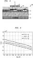
- FIG. 4 illustrates an exemplary silicon-based photodetector 30 formed in accordance with the present invention that addresses these limitations of the Patel et al. device.
- the elements that correspond to the prior art Patel et al. structure carry the same reference numerals.
- photodetector 30 further comprises a field plate 32 disposed above and separated from silicide strip 18.
- a dielectric region 34 separates field plate 32 from silicide strip 18.
- field plate 32 is easily incorporated into the standard CMOS process used for the fabrication of opto-electronic devices, where field plate 32 can be incorporated into the processing steps associated with the fabrication of the standard "metal 1" or "metal 2" layers.
- silicide strip 18 may itself be fabricated during a conventional set of process steps without the need to "modify” the process to create an ultra-thin silicide strip. This additional realization further simplifies the overall device fabrication process.
- a voltage V F is applied to field plate 32, which will induce an electric field across silicide strip 18.
- the presence of the electric field will, as discussed above, influence the direction of the momentum of the "hot” electrons and allow for a greater number of "hot” electrons to escape over the Schottky barrier and increase the generated photocurrent.
- the applied field across silicide strip 18 will preferentially shift the direction of momentum of these "hot” electrons in the direction normal to the silicon-silicide interface, the desired direction for movement of the carries over the barrier.
- the vertical separation S between field plate 32 and silicide strip 18 influences the responsivity of the device.
- field plate 32 if field plate 32 is positioned too close to the waveguiding structure, it will absorb a portion of the propagating signal, reducing the sensitivity of photodetector 30.
- a preferred metal layer to be used as field plate 32 is the "metal 1" layer of a standard CMOS process; however, a "metal 2" layer can also be used.
- the spacing between silicide strip 18 and field plate 32 is preferably on the order of 0.2 - 2.0 ⁇ m, with a preferred minimum spacing on the order of about 0.4 ⁇ m.
- FIG. 5 is a graph of the generated photocurrent as a function of bias voltage (V C -V A ) for three different values of V F .
- V F V A
- V F V A
- V F V A
- V F >V A V A
- Plot B is associated with the prior art arrangement, where the voltage applied to field plate 32 does not create an electric field along silicide strip 18.
- V F voltage present at anode 24 (the contact to SOI layer 16)
- the created electric field along silicide strip 18 will "add” to the existing field and thus adjust the moment of additional "hot” electrons to be in a direction essentially normal to the material interface. These additional "hot” electrons will then escape over the Schottky barrier and add to the created photocurrent.
- V F voltage to field plate 32 that actually subtracts from the nominal value and reduces the responsivity of photodetector 30. Decreasing the responsivity may be desired in situations where there is a need to "match" the responsivity to other system components.
- the responsivity of the photodetector of the present invention may be performed initially upon fabrication to provide a desired responsivity value, or may exist in the finished device as a 'tunable' element that is capable of being adjusted over time in various installations.
Landscapes
- Light Receiving Elements (AREA)
Claims (12)
- Infrarotfotodetektor (30) auf Siliciumbasis, integriert auf einem Silicium-auf-Isolator-(SOI)-Substrat (12, 14, 16) mit einem optischen Wellenleiter, wobei das SOI-Substrat (12, 14, 16) eine planare SOI-Oberflächenschicht (16) aufweist, wobei der optische Wellenleiter durch die planare SOI-Oberflächenschicht (16) gebildet wird, wobei der Infrarotfotodetektor (30) auf Siliciumbasis Folgendes umfasst:einen metallischen Streifen (18), der über einem Abschnitt der planaren SOI-Oberflächenschicht (16) in der Ausbreitungsrichtung eines optischen Signals entlang dem optischen Wellenleiter angeordnet ist, wobei der metallische Streifen (18) eine Schottky-Barriere mit dem optischen Wellenleiter bildet, wobei die Schottky-Barriere so ausgelegt ist, dass beim Gebrauch ein sich lateral entlang dem optischen Wellenleiter ausbreitendes optisches Signal in einer Richtung parallel zur Schottky-Barriere wandert;einen ersten ohmschen Kontakt (24), der auf der planaren SOI-Oberflächenschicht (16) in einem ersten Kontaktbereich angeordnet ist; undeinen zweiten ohmschen Kontakt (22), der auf dem metallischen Streifen (18) in einem zweiten Kontaktbereich angeordnet ist;dadurch gekennzeichnet, dass der Infrarotfotodetektor auf Siliciumbasis ferner eine Feldplattenelektrode (32) umfasst, die über den und separat von dem metallischen Streifen (18) angeordnet ist, wobei das Anlegen einer Spannung an die Feldplattenelektrode (32) das elektrische Feld entlang dem metallischen Streifen (18) modifiziert, um vorzugsweise das Moment von heißen Trägern zu leiten und die Anzahl von heißen Trägern zu beeinflussen, die die Schottky-Barriere überqueren, wodurch wiederum der durch den Infrarotfotodetektor auf Siliciumbasis erzeugte Fotostrom modifiziert wird.
- Infrarotfotodetektor auf Siliciumbasis nach Anspruch 1, wobei die Polarität der an die Feldplattenelektrode (32) angelegten Spannung so gesteuert wird, dass das Moment von heißen Trägern in einer Richtung nahezu normal mit Bezug auf die Grenzfläche zwischen der planaren SOI-Oberflächenschicht (16) und dem metallischen Streifen (18) vorzugsweise so geleitet wird, dass die Anzahl von heißen Trägern erhöht wird, die die Schottky-Barriere überqueren.
- Infrarotfotodetektor auf Siliciumbasis nach Anspruch 1, wobei die an die Feldplattenelektrode (32) angelegte Spannung so abgestimmt werden kann, dass die Anzahl von heißen Leitern justiert wird, die die Schottky-Barriere überqueren, und um dadurch die Empfindlichkeit des Fotodetektors zu justieren.
- Infrarotfotodetektor auf Siliciumbasis nach Anspruch 1, wobei der metallische Streifen (18) eine Schicht aus Silizidmaterial umfasst, die bei konventioneller CMOS-Verarbeitung angeordnet wird.
- Infrarotfotodetektor auf Siliciumbasis nach Anspruch 4, wobei die Schicht aus Silizidmaterial (18) in einem einzigen Schritt mit einer als Kontakt benutzten Silizidregion verarbeitet wird.
- Infrarotfotodetektor auf Siliciumbasis nach Anspruch 1, wobei die Feldplattenelektrode (32) einen Teil einer ersten Leiterschicht umfasst, die bei konventioneller CMOS-Verarbeitung angeordnet ist.
- Infrarotfotodetektor auf Siliciumbasis nach Anspruch 1, wobei die Feldplattenelektrode (32) einen Teil einer zweiten Leiterschicht umfasst, die bei konventioneller CMOS-Verarbeitung angeordnet wird.
- Infrarotfotodetektor auf Siliciumbasis nach Anspruch 1, wobei die planare SOI-Oberflächenschicht (16) n-dotiert ist und die heißen Träger heiße Elektronen umfassen.
- Infrarotfotodetektor auf Siliciumbasis nach Anspruch 1, wobei die planare SOI-Oberflächenschicht (16) p-dotiert ist und die heißen Träger heiße Löcher umfassen.
- Infrarotfotodetektor auf Siliciumbasis nach Anspruch 1, wobei die Feldplattenelektrode (32) von dem metallischen Streifen (18) um eine Distanz von maximal 2 µm getrennt ist.
- Infrarotfotodetektor auf Siliciumbasis nach Anspruch 1, wobei die Feldplattenelektrode (32) von dem metallischen Streifen (18) um eine Distanz von mindestens 0,2 µm getrennt ist.
- Infrarotfotodetektor auf Siliciumbasis nach Anspruch 1, wobei die Feldplattenelektrode (32) von dem metallischen Streifen (18) um eine Distanz von 0,4 µm getrennt ist.
Applications Claiming Priority (3)
| Application Number | Priority Date | Filing Date | Title |
|---|---|---|---|
| US33985510P | 2010-03-10 | 2010-03-10 | |
| US13/038,470 US8618625B2 (en) | 2010-03-10 | 2011-03-02 | Silicon-based schottky barrier detector with improved responsivity |
| PCT/US2011/026940 WO2011112406A2 (en) | 2010-03-10 | 2011-03-03 | Silicon-based schottky barrier detector with improved responsivity |
Publications (3)
| Publication Number | Publication Date |
|---|---|
| EP2545593A2 EP2545593A2 (de) | 2013-01-16 |
| EP2545593A4 EP2545593A4 (de) | 2017-12-27 |
| EP2545593B1 true EP2545593B1 (de) | 2018-12-12 |
Family
ID=44559154
Family Applications (1)
| Application Number | Title | Priority Date | Filing Date |
|---|---|---|---|
| EP11753819.9A Active EP2545593B1 (de) | 2010-03-10 | 2011-03-03 | Schottky-barrieren-detektor auf siliciumbasis mit verbesserter reaktivität |
Country Status (4)
| Country | Link |
|---|---|
| US (1) | US8618625B2 (de) |
| EP (1) | EP2545593B1 (de) |
| CN (1) | CN102782880B (de) |
| WO (1) | WO2011112406A2 (de) |
Families Citing this family (11)
| Publication number | Priority date | Publication date | Assignee | Title |
|---|---|---|---|---|
| CN102561295B (zh) * | 2012-01-09 | 2014-06-11 | 长沙理工大学 | 开挖膨胀土边坡坡面新生胀缩变形深度的观测及计算方法 |
| TWI493739B (zh) | 2013-06-05 | 2015-07-21 | Univ Nat Taiwan | 熱載子光電轉換裝置及其方法 |
| JP6228874B2 (ja) * | 2014-03-19 | 2017-11-08 | 株式会社日立製作所 | 半導体光素子 |
| EP3096180A1 (de) * | 2015-05-20 | 2016-11-23 | Philipps-Universität Marburg | Verfahren zur verbreiterung des frequenzspektrums einer elektromagnetischen welle und bauelement zu seiner realisierung |
| US9660117B1 (en) | 2016-09-19 | 2017-05-23 | Sharp Kabushiki Kaisha | Energy selective photodetector |
| CN106252454B (zh) | 2016-09-26 | 2017-08-25 | 京东方科技集团股份有限公司 | 一种光电探测器及光电探测装置 |
| CN110143563B (zh) * | 2018-05-16 | 2021-12-24 | 北京纳米能源与系统研究所 | 肖特基传感器系统 |
| CN110164981B (zh) * | 2018-05-16 | 2022-04-29 | 北京纳米能源与系统研究所 | 调节肖特基器件的肖特基势垒的方法 |
| CN109727849B (zh) * | 2018-12-17 | 2020-11-06 | 浙江大学 | 一种无串扰瞬时提高基于缺陷态机制的载流子耗尽型硅光功率监测器响应度的方法 |
| CN111947792B (zh) * | 2020-08-26 | 2022-10-11 | 合肥工业大学 | 一种基于二硒化钯/超薄硅/二硒化钯肖特基结的颜色探测系统及其制备方法 |
| CN112563345B (zh) * | 2020-12-09 | 2023-04-28 | 西安交通大学 | 一种匀化平面型光导开关电场的外导体电极结构及光导开关器件和方法 |
Family Cites Families (12)
| Publication number | Priority date | Publication date | Assignee | Title |
|---|---|---|---|---|
| JP2666889B2 (ja) | 1995-03-27 | 1997-10-22 | 工業技術院長 | 光電変換方法および光電変換素子 |
| US6211560B1 (en) | 1995-06-16 | 2001-04-03 | The United States Of America As Represented By The Secretary Of The Air Force | Voltage tunable schottky diode photoemissive infrared detector |
| EP0993053A1 (de) | 1998-10-09 | 2000-04-12 | STMicroelectronics S.r.l. | Infraroter Detektor mit einem integrierten Wellenleiter und Verfahren zu dessen Herstellung |
| JP2000164918A (ja) * | 1998-11-27 | 2000-06-16 | Mitsubishi Electric Corp | ショットキー接合型半導体光検出素子 |
| JP3684149B2 (ja) | 2000-11-15 | 2005-08-17 | 三菱電機株式会社 | 熱型赤外線検出器 |
| CA2365499C (en) | 2000-12-26 | 2011-02-15 | National Research Council Of Canada | High speed and high efficiency si-based photodetectors using waveguides formed with silicides for near ir applications |
| CA2514256A1 (en) * | 2003-03-04 | 2004-09-16 | Spectalis Corp. | Schottky barrier photodetectors |
| CA2546555A1 (en) * | 2003-11-20 | 2005-06-09 | Sioptical, Inc. | Silicon-based schottky barrier infrared optical detector |
| EP1829115A1 (de) * | 2004-12-24 | 2007-09-05 | Pirelli & C. S.p.A. | Fotodetektor in germanium auf silizium |
| JP2008051522A (ja) | 2006-08-22 | 2008-03-06 | Nec Tokin Corp | 熱型赤外線検出装置およびその製造方法 |
| JP4975669B2 (ja) | 2008-03-25 | 2012-07-11 | 株式会社東芝 | 赤外線検出器およびこの赤外線検出器を備えた固体撮像素子 |
| JP5264597B2 (ja) | 2008-04-03 | 2013-08-14 | 三菱電機株式会社 | 赤外線検出素子及び赤外線固体撮像装置 |
-
2011
- 2011-03-02 US US13/038,470 patent/US8618625B2/en active Active
- 2011-03-03 WO PCT/US2011/026940 patent/WO2011112406A2/en not_active Ceased
- 2011-03-03 EP EP11753819.9A patent/EP2545593B1/de active Active
- 2011-03-03 CN CN201180012674.8A patent/CN102782880B/zh not_active Expired - Fee Related
Non-Patent Citations (1)
| Title |
|---|
| None * |
Also Published As
| Publication number | Publication date |
|---|---|
| US8618625B2 (en) | 2013-12-31 |
| EP2545593A4 (de) | 2017-12-27 |
| WO2011112406A2 (en) | 2011-09-15 |
| CN102782880A (zh) | 2012-11-14 |
| EP2545593A2 (de) | 2013-01-16 |
| WO2011112406A3 (en) | 2011-12-08 |
| CN102782880B (zh) | 2015-09-23 |
| US20110221019A1 (en) | 2011-09-15 |
Similar Documents
| Publication | Publication Date | Title |
|---|---|---|
| US8618625B2 (en) | Silicon-based schottky barrier detector with improved responsivity | |
| Tran et al. | High performance Ge0. 89Sn0. 11 photodiodes for low-cost shortwave infrared imaging | |
| EP1716596B1 (de) | Auf silizium basierender optischer schottky-barrieren-infrarotdetektor | |
| US11682741B2 (en) | Electromagnetic wave detector | |
| US8618622B2 (en) | Photodetector optimized by metal texturing provided on the rear surface | |
| EP0651448B1 (de) | Verbesserter Metal-Semiconductor-Metal Photodetektor | |
| US20080105940A1 (en) | SOI-based inverse nanotaper optical detector | |
| JPH0469825B2 (de) | ||
| EP2022094A1 (de) | Detektion von plasmonen unter verwendung eines metallurgischen übergangs | |
| EP3480861B1 (de) | Lichtempfangendes element und nahinfrarotlichtdetektor | |
| US10128386B2 (en) | Semiconductor structure comprising an absorbing area placed in a focusing cavity | |
| US5969375A (en) | Infrared detector with non-cooled quantum well structure | |
| US9165967B2 (en) | Semiconductor structure able to receive electromagnetic radiation, semiconductor component and process for fabricating such a semiconductor structure | |
| US8410420B1 (en) | Semiconductor travelling-wave evanescent waveguide photodetector | |
| CA1228663A (en) | Photodetector with isolated avalanche region | |
| WO2009071916A1 (en) | Infrared avalanche photodiode structure with low excess noise and its manufacturing method | |
| US12578619B2 (en) | Current-assisted photonic demodulator with improved performances including intermediate electrodes | |
| JPS60247979A (ja) | 半導体光素子 | |
| JPH11330536A (ja) | 半導体受光素子 | |
| EP3480862A1 (de) | Lichtempfangendes element und nahinfrarotlichtdetektor | |
| Sednev et al. | Current–Voltage Characteristics of nBp Structures with Absorbing In0. 53Ga0. 47As Layer | |
| Wang et al. | A high-speed avalanche photodiode with large coupling tolerance | |
| EP2224497A1 (de) | Photodetektor beruhend auf der Detektion von Phononen | |
| US20230253516A1 (en) | Photodetector | |
| Smith et al. | A simplified fabrication process for HgCdTe photoconductive detectors using CH4/H2 reactive-ion-etching-induced blocking contacts |
Legal Events
| Date | Code | Title | Description |
|---|---|---|---|
| PUAI | Public reference made under article 153(3) epc to a published international application that has entered the european phase |
Free format text: ORIGINAL CODE: 0009012 |
|
| 17P | Request for examination filed |
Effective date: 20121010 |
|
| AK | Designated contracting states |
Kind code of ref document: A2 Designated state(s): AL AT BE BG CH CY CZ DE DK EE ES FI FR GB GR HR HU IE IS IT LI LT LU LV MC MK MT NL NO PL PT RO RS SE SI SK SM TR |
|
| DAX | Request for extension of the european patent (deleted) | ||
| RAP1 | Party data changed (applicant data changed or rights of an application transferred) |
Owner name: CISCO TECHNOLOGY, INC. |
|
| A4 | Supplementary search report drawn up and despatched |
Effective date: 20171127 |
|
| RIC1 | Information provided on ipc code assigned before grant |
Ipc: H01L 31/108 20060101AFI20171121BHEP Ipc: H01L 31/09 20060101ALI20171121BHEP |
|
| GRAP | Despatch of communication of intention to grant a patent |
Free format text: ORIGINAL CODE: EPIDOSNIGR1 |
|
| STAA | Information on the status of an ep patent application or granted ep patent |
Free format text: STATUS: GRANT OF PATENT IS INTENDED |
|
| INTG | Intention to grant announced |
Effective date: 20180703 |
|
| GRAS | Grant fee paid |
Free format text: ORIGINAL CODE: EPIDOSNIGR3 |
|
| GRAA | (expected) grant |
Free format text: ORIGINAL CODE: 0009210 |
|
| STAA | Information on the status of an ep patent application or granted ep patent |
Free format text: STATUS: THE PATENT HAS BEEN GRANTED |
|
| AK | Designated contracting states |
Kind code of ref document: B1 Designated state(s): AL AT BE BG CH CY CZ DE DK EE ES FI FR GB GR HR HU IE IS IT LI LT LU LV MC MK MT NL NO PL PT RO RS SE SI SK SM TR |
|
| REG | Reference to a national code |
Ref country code: GB Ref legal event code: FG4D |
|
| REG | Reference to a national code |
Ref country code: CH Ref legal event code: EP |
|
| REG | Reference to a national code |
Ref country code: AT Ref legal event code: REF Ref document number: 1077132 Country of ref document: AT Kind code of ref document: T Effective date: 20181215 |
|
| REG | Reference to a national code |
Ref country code: DE Ref legal event code: R096 Ref document number: 602011054749 Country of ref document: DE |
|
| REG | Reference to a national code |
Ref country code: IE Ref legal event code: FG4D |
|
| REG | Reference to a national code |
Ref country code: NL Ref legal event code: MP Effective date: 20181212 |
|
| REG | Reference to a national code |
Ref country code: LT Ref legal event code: MG4D |
|
| PG25 | Lapsed in a contracting state [announced via postgrant information from national office to epo] |
Ref country code: ES Free format text: LAPSE BECAUSE OF FAILURE TO SUBMIT A TRANSLATION OF THE DESCRIPTION OR TO PAY THE FEE WITHIN THE PRESCRIBED TIME-LIMIT Effective date: 20181212 Ref country code: NO Free format text: LAPSE BECAUSE OF FAILURE TO SUBMIT A TRANSLATION OF THE DESCRIPTION OR TO PAY THE FEE WITHIN THE PRESCRIBED TIME-LIMIT Effective date: 20190312 Ref country code: HR Free format text: LAPSE BECAUSE OF FAILURE TO SUBMIT A TRANSLATION OF THE DESCRIPTION OR TO PAY THE FEE WITHIN THE PRESCRIBED TIME-LIMIT Effective date: 20181212 Ref country code: LT Free format text: LAPSE BECAUSE OF FAILURE TO SUBMIT A TRANSLATION OF THE DESCRIPTION OR TO PAY THE FEE WITHIN THE PRESCRIBED TIME-LIMIT Effective date: 20181212 Ref country code: BG Free format text: LAPSE BECAUSE OF FAILURE TO SUBMIT A TRANSLATION OF THE DESCRIPTION OR TO PAY THE FEE WITHIN THE PRESCRIBED TIME-LIMIT Effective date: 20190312 Ref country code: FI Free format text: LAPSE BECAUSE OF FAILURE TO SUBMIT A TRANSLATION OF THE DESCRIPTION OR TO PAY THE FEE WITHIN THE PRESCRIBED TIME-LIMIT Effective date: 20181212 Ref country code: LV Free format text: LAPSE BECAUSE OF FAILURE TO SUBMIT A TRANSLATION OF THE DESCRIPTION OR TO PAY THE FEE WITHIN THE PRESCRIBED TIME-LIMIT Effective date: 20181212 |
|
| REG | Reference to a national code |
Ref country code: AT Ref legal event code: MK05 Ref document number: 1077132 Country of ref document: AT Kind code of ref document: T Effective date: 20181212 |
|
| PG25 | Lapsed in a contracting state [announced via postgrant information from national office to epo] |
Ref country code: AL Free format text: LAPSE BECAUSE OF FAILURE TO SUBMIT A TRANSLATION OF THE DESCRIPTION OR TO PAY THE FEE WITHIN THE PRESCRIBED TIME-LIMIT Effective date: 20181212 Ref country code: SE Free format text: LAPSE BECAUSE OF FAILURE TO SUBMIT A TRANSLATION OF THE DESCRIPTION OR TO PAY THE FEE WITHIN THE PRESCRIBED TIME-LIMIT Effective date: 20181212 Ref country code: RS Free format text: LAPSE BECAUSE OF FAILURE TO SUBMIT A TRANSLATION OF THE DESCRIPTION OR TO PAY THE FEE WITHIN THE PRESCRIBED TIME-LIMIT Effective date: 20181212 Ref country code: GR Free format text: LAPSE BECAUSE OF FAILURE TO SUBMIT A TRANSLATION OF THE DESCRIPTION OR TO PAY THE FEE WITHIN THE PRESCRIBED TIME-LIMIT Effective date: 20190313 |
|
| PG25 | Lapsed in a contracting state [announced via postgrant information from national office to epo] |
Ref country code: NL Free format text: LAPSE BECAUSE OF FAILURE TO SUBMIT A TRANSLATION OF THE DESCRIPTION OR TO PAY THE FEE WITHIN THE PRESCRIBED TIME-LIMIT Effective date: 20181212 |
|
| PG25 | Lapsed in a contracting state [announced via postgrant information from national office to epo] |
Ref country code: CZ Free format text: LAPSE BECAUSE OF FAILURE TO SUBMIT A TRANSLATION OF THE DESCRIPTION OR TO PAY THE FEE WITHIN THE PRESCRIBED TIME-LIMIT Effective date: 20181212 Ref country code: IT Free format text: LAPSE BECAUSE OF FAILURE TO SUBMIT A TRANSLATION OF THE DESCRIPTION OR TO PAY THE FEE WITHIN THE PRESCRIBED TIME-LIMIT Effective date: 20181212 Ref country code: PL Free format text: LAPSE BECAUSE OF FAILURE TO SUBMIT A TRANSLATION OF THE DESCRIPTION OR TO PAY THE FEE WITHIN THE PRESCRIBED TIME-LIMIT Effective date: 20181212 Ref country code: PT Free format text: LAPSE BECAUSE OF FAILURE TO SUBMIT A TRANSLATION OF THE DESCRIPTION OR TO PAY THE FEE WITHIN THE PRESCRIBED TIME-LIMIT Effective date: 20190412 |
|
| PG25 | Lapsed in a contracting state [announced via postgrant information from national office to epo] |
Ref country code: EE Free format text: LAPSE BECAUSE OF FAILURE TO SUBMIT A TRANSLATION OF THE DESCRIPTION OR TO PAY THE FEE WITHIN THE PRESCRIBED TIME-LIMIT Effective date: 20181212 Ref country code: SM Free format text: LAPSE BECAUSE OF FAILURE TO SUBMIT A TRANSLATION OF THE DESCRIPTION OR TO PAY THE FEE WITHIN THE PRESCRIBED TIME-LIMIT Effective date: 20181212 Ref country code: IS Free format text: LAPSE BECAUSE OF FAILURE TO SUBMIT A TRANSLATION OF THE DESCRIPTION OR TO PAY THE FEE WITHIN THE PRESCRIBED TIME-LIMIT Effective date: 20190412 Ref country code: RO Free format text: LAPSE BECAUSE OF FAILURE TO SUBMIT A TRANSLATION OF THE DESCRIPTION OR TO PAY THE FEE WITHIN THE PRESCRIBED TIME-LIMIT Effective date: 20181212 Ref country code: SK Free format text: LAPSE BECAUSE OF FAILURE TO SUBMIT A TRANSLATION OF THE DESCRIPTION OR TO PAY THE FEE WITHIN THE PRESCRIBED TIME-LIMIT Effective date: 20181212 |
|
| REG | Reference to a national code |
Ref country code: DE Ref legal event code: R097 Ref document number: 602011054749 Country of ref document: DE |
|
| PLBE | No opposition filed within time limit |
Free format text: ORIGINAL CODE: 0009261 |
|
| STAA | Information on the status of an ep patent application or granted ep patent |
Free format text: STATUS: NO OPPOSITION FILED WITHIN TIME LIMIT |
|
| PG25 | Lapsed in a contracting state [announced via postgrant information from national office to epo] |
Ref country code: AT Free format text: LAPSE BECAUSE OF FAILURE TO SUBMIT A TRANSLATION OF THE DESCRIPTION OR TO PAY THE FEE WITHIN THE PRESCRIBED TIME-LIMIT Effective date: 20181212 Ref country code: DK Free format text: LAPSE BECAUSE OF FAILURE TO SUBMIT A TRANSLATION OF THE DESCRIPTION OR TO PAY THE FEE WITHIN THE PRESCRIBED TIME-LIMIT Effective date: 20181212 Ref country code: MC Free format text: LAPSE BECAUSE OF FAILURE TO SUBMIT A TRANSLATION OF THE DESCRIPTION OR TO PAY THE FEE WITHIN THE PRESCRIBED TIME-LIMIT Effective date: 20181212 Ref country code: SI Free format text: LAPSE BECAUSE OF FAILURE TO SUBMIT A TRANSLATION OF THE DESCRIPTION OR TO PAY THE FEE WITHIN THE PRESCRIBED TIME-LIMIT Effective date: 20181212 |
|
| REG | Reference to a national code |
Ref country code: CH Ref legal event code: PL |
|
| 26N | No opposition filed |
Effective date: 20190913 |
|
| PG25 | Lapsed in a contracting state [announced via postgrant information from national office to epo] |
Ref country code: LU Free format text: LAPSE BECAUSE OF NON-PAYMENT OF DUE FEES Effective date: 20190303 |
|
| REG | Reference to a national code |
Ref country code: BE Ref legal event code: MM Effective date: 20190331 |
|
| PG25 | Lapsed in a contracting state [announced via postgrant information from national office to epo] |
Ref country code: CH Free format text: LAPSE BECAUSE OF NON-PAYMENT OF DUE FEES Effective date: 20190331 Ref country code: IE Free format text: LAPSE BECAUSE OF NON-PAYMENT OF DUE FEES Effective date: 20190303 Ref country code: LI Free format text: LAPSE BECAUSE OF NON-PAYMENT OF DUE FEES Effective date: 20190331 |
|
| PG25 | Lapsed in a contracting state [announced via postgrant information from national office to epo] |
Ref country code: BE Free format text: LAPSE BECAUSE OF NON-PAYMENT OF DUE FEES Effective date: 20190331 |
|
| PG25 | Lapsed in a contracting state [announced via postgrant information from national office to epo] |
Ref country code: TR Free format text: LAPSE BECAUSE OF FAILURE TO SUBMIT A TRANSLATION OF THE DESCRIPTION OR TO PAY THE FEE WITHIN THE PRESCRIBED TIME-LIMIT Effective date: 20181212 |
|
| PG25 | Lapsed in a contracting state [announced via postgrant information from national office to epo] |
Ref country code: MT Free format text: LAPSE BECAUSE OF NON-PAYMENT OF DUE FEES Effective date: 20190303 |
|
| PG25 | Lapsed in a contracting state [announced via postgrant information from national office to epo] |
Ref country code: CY Free format text: LAPSE BECAUSE OF FAILURE TO SUBMIT A TRANSLATION OF THE DESCRIPTION OR TO PAY THE FEE WITHIN THE PRESCRIBED TIME-LIMIT Effective date: 20181212 |
|
| PG25 | Lapsed in a contracting state [announced via postgrant information from national office to epo] |
Ref country code: HU Free format text: LAPSE BECAUSE OF FAILURE TO SUBMIT A TRANSLATION OF THE DESCRIPTION OR TO PAY THE FEE WITHIN THE PRESCRIBED TIME-LIMIT; INVALID AB INITIO Effective date: 20110303 |
|
| PG25 | Lapsed in a contracting state [announced via postgrant information from national office to epo] |
Ref country code: MK Free format text: LAPSE BECAUSE OF FAILURE TO SUBMIT A TRANSLATION OF THE DESCRIPTION OR TO PAY THE FEE WITHIN THE PRESCRIBED TIME-LIMIT Effective date: 20181212 |
|
| P01 | Opt-out of the competence of the unified patent court (upc) registered |
Effective date: 20230525 |
|
| REG | Reference to a national code |
Ref country code: DE Ref legal event code: R079 Ref document number: 602011054749 Country of ref document: DE Free format text: PREVIOUS MAIN CLASS: H01L0031108000 Ipc: H10F0030227000 |
|
| PGFP | Annual fee paid to national office [announced via postgrant information from national office to epo] |
Ref country code: GB Payment date: 20260224 Year of fee payment: 16 |
|
| PGFP | Annual fee paid to national office [announced via postgrant information from national office to epo] |
Ref country code: DE Payment date: 20260217 Year of fee payment: 16 |
|
| PGFP | Annual fee paid to national office [announced via postgrant information from national office to epo] |
Ref country code: FR Payment date: 20260305 Year of fee payment: 16 |