EP2546889B1 - Solarzellenbaugruppe und Verfahren zur Herstellung einer Solarzellenbaugruppe - Google Patents
Solarzellenbaugruppe und Verfahren zur Herstellung einer Solarzellenbaugruppe Download PDFInfo
- Publication number
- EP2546889B1 EP2546889B1 EP11005666.0A EP11005666A EP2546889B1 EP 2546889 B1 EP2546889 B1 EP 2546889B1 EP 11005666 A EP11005666 A EP 11005666A EP 2546889 B1 EP2546889 B1 EP 2546889B1
- Authority
- EP
- European Patent Office
- Prior art keywords
- solar cell
- electric contact
- interconnector
- contact pad
- substrate
- Prior art date
- Legal status (The legal status is an assumption and is not a legal conclusion. Google has not performed a legal analysis and makes no representation as to the accuracy of the status listed.)
- Active
Links
Images


Classifications
-
- H—ELECTRICITY
- H10—SEMICONDUCTOR DEVICES; ELECTRIC SOLID-STATE DEVICES NOT OTHERWISE PROVIDED FOR
- H10F—INORGANIC SEMICONDUCTOR DEVICES SENSITIVE TO INFRARED RADIATION, LIGHT, ELECTROMAGNETIC RADIATION OF SHORTER WAVELENGTH OR CORPUSCULAR RADIATION
- H10F19/00—Integrated devices, or assemblies of multiple devices, comprising at least one photovoltaic cell covered by group H10F10/00, e.g. photovoltaic modules
- H10F19/90—Structures for connecting between photovoltaic cells, e.g. interconnections or insulating spacers
- H10F19/902—Structures for connecting between photovoltaic cells, e.g. interconnections or insulating spacers for series or parallel connection of photovoltaic cells
- H10F19/904—Structures for connecting between photovoltaic cells, e.g. interconnections or insulating spacers for series or parallel connection of photovoltaic cells characterised by the shapes of the structures
-
- H—ELECTRICITY
- H10—SEMICONDUCTOR DEVICES; ELECTRIC SOLID-STATE DEVICES NOT OTHERWISE PROVIDED FOR
- H10F—INORGANIC SEMICONDUCTOR DEVICES SENSITIVE TO INFRARED RADIATION, LIGHT, ELECTROMAGNETIC RADIATION OF SHORTER WAVELENGTH OR CORPUSCULAR RADIATION
- H10F10/00—Individual photovoltaic cells, e.g. solar cells
- H10F10/10—Individual photovoltaic cells, e.g. solar cells having potential barriers
- H10F10/14—Photovoltaic cells having only PN homojunction potential barriers
- H10F10/142—Photovoltaic cells having only PN homojunction potential barriers comprising multiple PN homojunctions, e.g. tandem cells
-
- H—ELECTRICITY
- H10—SEMICONDUCTOR DEVICES; ELECTRIC SOLID-STATE DEVICES NOT OTHERWISE PROVIDED FOR
- H10F—INORGANIC SEMICONDUCTOR DEVICES SENSITIVE TO INFRARED RADIATION, LIGHT, ELECTROMAGNETIC RADIATION OF SHORTER WAVELENGTH OR CORPUSCULAR RADIATION
- H10F19/00—Integrated devices, or assemblies of multiple devices, comprising at least one photovoltaic cell covered by group H10F10/00, e.g. photovoltaic modules
- H10F19/70—Integrated devices, or assemblies of multiple devices, comprising at least one photovoltaic cell covered by group H10F10/00, e.g. photovoltaic modules comprising bypass diodes
- H10F19/75—Integrated devices, or assemblies of multiple devices, comprising at least one photovoltaic cell covered by group H10F10/00, e.g. photovoltaic modules comprising bypass diodes the bypass diodes being integrated or directly associated with the photovoltaic cells, e.g. formed in or on the same substrate
-
- H—ELECTRICITY
- H10—SEMICONDUCTOR DEVICES; ELECTRIC SOLID-STATE DEVICES NOT OTHERWISE PROVIDED FOR
- H10F—INORGANIC SEMICONDUCTOR DEVICES SENSITIVE TO INFRARED RADIATION, LIGHT, ELECTROMAGNETIC RADIATION OF SHORTER WAVELENGTH OR CORPUSCULAR RADIATION
- H10F19/00—Integrated devices, or assemblies of multiple devices, comprising at least one photovoltaic cell covered by group H10F10/00, e.g. photovoltaic modules
- H10F19/80—Encapsulations or containers for integrated devices, or assemblies of multiple devices, having photovoltaic cells
-
- H—ELECTRICITY
- H10—SEMICONDUCTOR DEVICES; ELECTRIC SOLID-STATE DEVICES NOT OTHERWISE PROVIDED FOR
- H10F—INORGANIC SEMICONDUCTOR DEVICES SENSITIVE TO INFRARED RADIATION, LIGHT, ELECTROMAGNETIC RADIATION OF SHORTER WAVELENGTH OR CORPUSCULAR RADIATION
- H10F19/00—Integrated devices, or assemblies of multiple devices, comprising at least one photovoltaic cell covered by group H10F10/00, e.g. photovoltaic modules
- H10F19/90—Structures for connecting between photovoltaic cells, e.g. interconnections or insulating spacers
- H10F19/902—Structures for connecting between photovoltaic cells, e.g. interconnections or insulating spacers for series or parallel connection of photovoltaic cells
- H10F19/908—Structures for connecting between photovoltaic cells, e.g. interconnections or insulating spacers for series or parallel connection of photovoltaic cells for back-contact photovoltaic cells
-
- H—ELECTRICITY
- H10—SEMICONDUCTOR DEVICES; ELECTRIC SOLID-STATE DEVICES NOT OTHERWISE PROVIDED FOR
- H10F—INORGANIC SEMICONDUCTOR DEVICES SENSITIVE TO INFRARED RADIATION, LIGHT, ELECTROMAGNETIC RADIATION OF SHORTER WAVELENGTH OR CORPUSCULAR RADIATION
- H10F77/00—Constructional details of devices covered by this subclass
- H10F77/20—Electrodes
- H10F77/206—Electrodes for devices having potential barriers
- H10F77/211—Electrodes for devices having potential barriers for photovoltaic cells
-
- H—ELECTRICITY
- H10—SEMICONDUCTOR DEVICES; ELECTRIC SOLID-STATE DEVICES NOT OTHERWISE PROVIDED FOR
- H10F—INORGANIC SEMICONDUCTOR DEVICES SENSITIVE TO INFRARED RADIATION, LIGHT, ELECTROMAGNETIC RADIATION OF SHORTER WAVELENGTH OR CORPUSCULAR RADIATION
- H10F77/00—Constructional details of devices covered by this subclass
- H10F77/10—Semiconductor bodies
- H10F77/12—Active materials
- H10F77/124—Active materials comprising only Group III-V materials, e.g. GaAs
-
- Y—GENERAL TAGGING OF NEW TECHNOLOGICAL DEVELOPMENTS; GENERAL TAGGING OF CROSS-SECTIONAL TECHNOLOGIES SPANNING OVER SEVERAL SECTIONS OF THE IPC; TECHNICAL SUBJECTS COVERED BY FORMER USPC CROSS-REFERENCE ART COLLECTIONS [XRACs] AND DIGESTS
- Y02—TECHNOLOGIES OR APPLICATIONS FOR MITIGATION OR ADAPTATION AGAINST CLIMATE CHANGE
- Y02E—REDUCTION OF GREENHOUSE GAS [GHG] EMISSIONS, RELATED TO ENERGY GENERATION, TRANSMISSION OR DISTRIBUTION
- Y02E10/00—Energy generation through renewable energy sources
- Y02E10/50—Photovoltaic [PV] energy
- Y02E10/544—Solar cells from Group III-V materials
-
- Y—GENERAL TAGGING OF NEW TECHNOLOGICAL DEVELOPMENTS; GENERAL TAGGING OF CROSS-SECTIONAL TECHNOLOGIES SPANNING OVER SEVERAL SECTIONS OF THE IPC; TECHNICAL SUBJECTS COVERED BY FORMER USPC CROSS-REFERENCE ART COLLECTIONS [XRACs] AND DIGESTS
- Y02—TECHNOLOGIES OR APPLICATIONS FOR MITIGATION OR ADAPTATION AGAINST CLIMATE CHANGE
- Y02P—CLIMATE CHANGE MITIGATION TECHNOLOGIES IN THE PRODUCTION OR PROCESSING OF GOODS
- Y02P70/00—Climate change mitigation technologies in the production process for final industrial or consumer products
- Y02P70/50—Manufacturing or production processes characterised by the final manufactured product
Definitions
- the present invention is directed to a solar cell as defined in the preamble of claim 1. It is further directed to a solar cell assembly of such solar cells and to a method of manufacturing a solar cell assembly.
- the present invention comprises a new efficient method to manufacture a solar cell with electrical contacts of both polarities on the front surface, improved design features for a spatial arrangement of a plurality of this type of solar cells into a photovoltaic assembly as well as an automated manufacturing flow possible with this arrangement.
- the features of this invention which is mainly focused on solar cell and solar cell assemblies for space use, but not necessarily limited to it, will become evident in a comparison with the prior art.
- multi-junction solar cells based on III-V semiconductors with current efficiencies between 25 - 30 % are used. Further efficiency increase is likely to occur with adapted designs in the future.
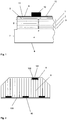
- FIG.1 A cross section through a prior art triple junction (TJ) cell is illustrated in Fig.1 .
- the vertical dimensions are not to scale and laterally the cell extends further to the right.
- a Germanium wafer 4 typically 80 - 150 ⁇ m thick, serves as the substrate of the cell.
- a p-n-junction 3 is created, some ⁇ m from the wafer front surface by diffusion.
- two more p-n-junctions 1, 2 are grown from III-V semiconductor materials. It is implicitly understood here as well as in the following that tunnel junctions are included between each p-n-junction.
- several additional layers functioning for example as back surface fields, buffer layers, reflectors are included in the actual device.
- the top most cell layer is passivated on the surface by a transparent window layer 5.
- the three p-n-junctions are located within a depth of approximately 10 ⁇ m from the cell surface.
- the cell shape has then to be isolated from the usually circular Germanium wafer and the epitaxially grown junctions on top of it.
- the cell circumference is defined by etching a so called “mesa" groove 6, sufficiently deep (e.g. 10 ⁇ m in this example) to separate all three p-n-junctions.
- the remaining electrically inactive Germanium wafer is then separated mechanically by dicing, i.e. by sawing along a cut line 7.
- the rear side contact 8 is usually completely metalized with any metal system able to form an ohmic contact to the cell.
- the front side contact 9 is produced similarly. Due to the fact, however, that light has to enter the cell from the front, the front side contact is shaped in the form of narrow grid fingers 100 ( Fig. 2 ), which are connected among each other and finally to a number of front side contact pads 10 used for the external cell connection. A typical layout is illustrated in Fig. 2 .
- the so called cap layer 11 Underneath the front side grid another doped semiconductor layer is present, the so called cap layer 11, primarily to serve as additional protection of the cell during attachment of external electrical connections on the contact pads 10 by methods such as soldering or welding. To minimize light reflections, an antireflection coating 12 is deposited on the cell front side.
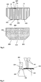
- the primary element for solar arrays in space is a connection of typical 30 or 60 cells in series for required bus voltages of 50 or 100 V.
- strings are then connected in parallel at their ends with the inclusion of blocking diodes to sections and deliver currents around 10 A.
- the strings are placed on a common insulating substrate 201. Together with the electrical parallel connection of the strings this forms the photovoltaic assembly (PVA).
- Solar arrays for space use are for example sandwich panels with a carbon fibre face sheet and an aluminium honeycomb core with a Kapton front side insulation. These substrates have large thermal expansion mismatch relative to the cells.
- the gap 202 between two cells varies by several 10 ⁇ m, exposing any electrical connection between two cells to significant cyclic stress.
- 10 - 20 ⁇ m thick metal foils like Silver (Ag), Gold (Au), silver-plated Molybdenum (Mo), silver-plated nickel-cobalt ferrous alloy (e.g. known under the trademark "Kovar” and having a low coefficient of thermal expansion), etc. to bridge the gap between two cells.
- the electrical series connection naturally has to be performed from the front side contact pad 10 of one cell to the rear side 203 of the adjacent cell.
- the interconnector 204 is S-shaped, protruding significantly above the cell.
- a metal contact 102 By depositing a metal contact 102 on top of it, a (-) contact is provided.
- a (-) contact is provided.
- several of these diode p-n-junctions can be etched away to reduce the diode voltage. Due to the fact that the diode created out of cell material in this fashion has the same polarity as the cell, it cannot protect the cell it is located in. Rather an electrical connection has to be made by another S shaped interconnector 205 from the front side contact of the diode 102 to the rear side 206 of the neighbouring cell.
- the interconnectors of diode and cell are welded to the cell first. Then the cover glass is bonded onto the cell to form a cover integrated cell (CIC). These steps are usually fully automated. Then the CICs have to be positioned with the cover glass facing downwards onto a suitable welding plate and the diode and power interconnectors have to be aligned on the appropriate cell rear side, which is a cumbersome manual process. Note that diode and power interconnectors go to the rear side of different cells. Then all rear side interconnections are performed, again automatically, e.g. by welding.
- CIC cover integrated cell
- the string of cells created in this way is turned upside down again, by affixing it to a temporary transport plate. Then it is placed with the cover glass front side onto an adhesive foil, which supports the strings during the lay down process.
- an adhesive foil which supports the strings during the lay down process.
- a room temperature curing silicone adhesive is applied onto the cell rear side, for example by screen printing, which assures a well defined adhesive thickness.
- the strings are placed onto the support structure.
- pressure is applied onto the cells by enclosing the cell in an appropriate fashion and evacuating this area.
- the self adhesive foil is removed from the front side of the CICs.
- EP 1 693 899 A2 is directed to a solar cell arrangement comprising a plurality of solar cells which are electrically interconnected wherein each solar cell has its electrical contact pads for both polarities provided on the front side of the solar cell. After the plurality of solar cells have been electrically interconnected a transparent protective member of glass is adhered to the surface of the sunlight entering side of the solar cells.
- DE 10 2007 011 403 A1 discloses a similar embodiment of a plurality of electrically interconnected solar cells which are mounted to a rigid carrier structure and which are covered by a transparent front shield.
- US 2002/0144724 A1 discloses a solar cell having a front-mounted bypass diode wherein the solar cell is provided with at least two front surface contacts of different polarity. This known solar cell has no protection against any destroying radiation so that this solar cell cannot be used in space.
- EP 1 030 376 A1 is directed to a solar cell panel comprising a plurality of electrically interconnected solar cells which are together covered by a common cover glass sheet.
- the cover glass sheet has slit-like cuts along boundary lines between the solar cells on one of the cover glass surfaces. These slit-like cuts allow the cover glass to break between the adjacent solar cells when the cover glass sheet is subjected to an excessive stress.
- WO 2010/116973 , WO 99/60606 and US 6,248,948 B1 are also directed to solar cell arrangements in which the single solar cells are electrically connected together and wherein the solar cells are commonly covered by a cover glass. Also these solar cell arrangements are due to their large cover glass not suitable for use in space.
- solar cell assembly denotes a spatial arrangement of a plurality of solar cells or CICs, i.e. solar cells equipped with interconnector and cover glass.
- the first object of the invention which is directed to a solar cell assembly is achieved by a solar cell assembly with the features of claim 1 or alternatively with the features of claim 2.
- the object of the present invention which is directed to the solar cell assembly is solved in case of an assembly of at least three interconnectable solar cells according to the features of claim 1 when the solar cells form a row of solar cells and alternatively by a solar cell assembly of at least three interconnectable solar cells with the features of claim 2 when the solar cells form an array of solar cells.
- a cover glass is provided on the front surface of the front layer and said cover glass is provided with cut-outs at the positions of the second electric contact point, the cut-outs having preferably the same size as a contact pad of the electric contact. The provision of this cover glass limits radiation damage of the cells when the solar cell is used in space.
- first and second electric contact pads of the first and second electric contacts, respectively, of each solar cell are positioned so that a first electric contact pad of a first solar cell is placed close to a second electric contact pad of an adjacent solar cell and a second electric contact pad of said first solar cell is placed close to a first electric contact pad of a further adjacent solar cell when said solar cells form a row of solar cells.
- the first and second electric contacts pads of the first and second electric contacts, respectively, of each solar cell are positioned so that a first electric contact pad of a first solar cell is placed close to a second electric contact pad of an adjacent solar cell and a second electric contact pad of said first solar cell is placed close to a first electric contact pad of a further adjacent solar cell when said solar cells form an array of solar cells;
- interconnectors are provided to connect each first electric contact pad of said first solar cell with the adjacent second electric contact pad of said adjacent solar cell and to connect each second electric contact pad of said first solar cell with the adjacent first electric contact pad of said further adjacent solar cell and the size of each interconnector is such that no element of the interconnector protrudes from the front surfaces of the solar cells connected by said interconnector.
- each interconnector is provided with a cover member covering the front surface of the interconnector. This feature protects also the connector region against ion erosion (sputtering) from ion thrusters.
- cover member covering the front surface to the interconnector between two solar cells is an important inventive feature because this cover member closes the gap between the glass covers of two adjacent solar cells above the interconnector.
- This modular structure of the cover glasses and cover members provides a certain flexibility to the whole solar cell assembly on the one hand and protects the solar cells and the interconnectors between the solar cells against destructive space radiation.
- At least one intermediate layer comprising a p-n-junction is provided between said substrate and said front layer wherein said p-n-junction separates the at least one intermediate layer into a front portion having said first doping and a rear portion having said second doping and wherein said intermediate layer front portion is averted from said substrate front portion.
- said groove is provided on a lateral side of the solar cell so that it also opens to the lateral side.
- This embodiment allows a lateral contacting of the solar cell.
- front surface of the front layer is at least partially provided with an antireflection coating.
- said bottom surface of the groove is provided around a contact pad of said second electric contact point at least partially with an antireflection coating.
- said solar cell is a III-V triple junction cell wherein said substrate is a Germanium wafer.
- said interconnectors are formed in U-shape or W-shape configuration. Such a bent interconnector is able to compensate thermal extensions.
- each interconnector comprises a plurality of grid fingers, each of which is contacted separately to the associated electric contact pad.
- This type of connector provides redundancy against disconnection because each grid finger is connected separately to the associated contact pad.
- the front surface of said cover glass is provided with a conductive coating which is connected to a metalized portion of a side wall of the cover glass adjacent to the groove accommodating one of the second electric contact pads and said metalized portion is electrically connected to said first electric contact pad.
- the free end of the interconnector is bent towards the front side of the solar cell (e.g. upwardly bent), and the bent portion of the interconnector electrically contacts the metalized portion of the side wall when the interconnector is fixed to said electric contact pad.
- the bent portion of the interconnector is formed with grid fingers at the free end thereof. This design provides redundancy as at least one of the grid fingers needs to be in contact with the metalized portion.
- the bent portion is integrally formed in the region of the elbow-like bending and connects the grid fingers of the bent portion and, if so provided, also the grid fingers which are provided to be contacted to the contact pad.
- the object directed to the manufacturing method of a solar cell assembly is achieved by a method according to claim 16. This method comprises the steps of
- This inventive manufacturing method for a solar cell assembly allows fast and reliable automatic manufacturing of the solar cell assembly.
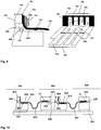
- the solar cell C shown in Fig. 4 is made of a semiconductor substrate 4 having a front surface 4' and a rear surface 4".
- a first p-n-junction 3 is provided in the substrate 4 close to the front surface 4' thereof.
- the p-n-junction 3 separates the substrate into a front portion having a first doping n and a rear portion having a second doping p.
- Fig. 4 illustrates the proposed technique of a solar cell C according to this invention to establish a contact point 304 of a rear side contact 8 on the cell front side.
- the contact point 304 is electrically connected via a rear portion 303 of the substrate 4 to the rear side contact 8 by exploiting the high conductivity of the Germanium substrate 4.
- the drawing is not to scale and the solar cell C shown in Fig. 4 serves illustration purposes only. The invention is in no way limited to this particular cell type or geometry.
- Features of the solar cell C according to the invention which resemble features of the prior art solar cell shown in Figs. 1 and 2 have been allotted the same reference numerals and for their description reference is made to the description of Figs. 1 and 2 .
- a front layer 1' comprising a p-n-junction 1 is provided on the front surface of the substrate 4, wherein the p-n-junction separates the front layer 1' into a front portion having the first doping n and a rear portion having the second doping p.
- the front layer's front portion is averted from the substrate front portion 306.
- An intermediate layer 2' comprising a p-n-junction 2 is provided between said substrate 4 and said front layer 1'.
- the p-n-junction separates the intermediate layer 2' into a front portion having the first doping n and a rear portion having the second doping p.
- the intermediate layer's front portion is averted from the substrate front portion.
- First electric contacts 9 are provided on the front side C' of the solar cell C in the form of grid fingers and are electrically connected to the front portion of the front layer 1'. These grid finger contacts are connected to a plurality of contact pads 10 which are disposed on a lateral side of the front surface of the solar cell C.
- Second electric contact pads 304' forming the contact points 304 are provided so that they are accessible form the front side C' of the solar cell C as will be described below. These second electric contact pads 304' are electrically connected to the rear portion 303 of the substrate 4. The second electric contact pads 304' are placed on the bottom surface of a groove 305 which opens to the front side C' of the solar cell C and which extends to the rear portion 303 of the substrate 4. Groove 305 opens also to lateral side 7' of cell C.
- the epitaxy is etched at 301 to about 10 ⁇ m, whereas the width of the groove 305 forming a contact pad area 302 for the contact pad 304' of contact point 304 is a one hundred times as large.
- the height 7 of the remaining wafer is in the order of 100 ⁇ m.
- the first element of this invention involves an efficient way to establish an independent (+) contact point 304 at the location 300 on the cell front side C' as well, next to the (-) contact pad 10 already present there.
- the contact which is in the prior art present on the cell rear side is moved to the front side C'.
- This is achieved as shown in Fig. 4 by relying on the conductivity of the p doped Germanium wafer 4 itself.
- the polarity of the contacts and the associated doping (p or n) in Fig. 4 just serves as an example. Opposite polarities are of course feasible as well.
- the entire epitaxy is etched away to form the groove 305 of a height 301 down to the p doped rear portion 303 of the Germanium substrate 4.
- the same etch processes used to establish the mesa groove 6 at the cell edge or to isolate the integrated diode can be applied here as well.
- the metal contact pad 304' is then deposited on the p doped rear portion 303 of the Germanium substrate 4 and serves as a contact pad for an external cell connector.
- both front side contacts can also be deposited in on step on the cell front side.
- the Germanium substrate in state of the art triple junction cells is fairly highly doped, resulting in specific resistances in the 10 m ⁇ cm range (Ref.: C. G. Zimmermann, Journal of Applied Physics, 100, 023714, 2006 ).
- the rear side metallization at rear side contact 8 which is typically equally thick as the front side metallization at front side contact 9 to ensure the same properties at the contact pad location, might be in addition reduced in thickness, depending on the amount of additional ohmic losses tolerable.
- the antireflection coating 12 in the (+) contact area 302 is optional.
- the cropped corner region can be a preferred location of the contact pads or welding pads. At these locations the possibility exists to use part of the circular wafer region unsuitable as solar cell itself for the contact pad and thus minimize the loss in additional cell area.
- Fig. 5 a spatial arrangement of the additional (+) contacts 400, 401 on the cell front side together with an adapted layout of a cover glass 403 is shown.
- (+) contacts 400 for a 8 x 4 cm 2 sized triple junction cell with three (-) contact pads 10 and an integrated diode 102 is illustrated in Fig. 5 .
- a fourth (+) contact 401 is required for interconnection of the diode of the neighbouring cell.
- 10 mm 2 of active cell area are etched away for a 7 mm 2 contact pad, which ensures sufficient distance of the contact pad metal to the open p-n-junctions, 1.3 % of the cell area is lost due to the placement of the (+) contacts on the cell front side.
- the horizontal collecting gridline 100 has to be shaped around (see at 402) the contact pad required for the optional diode contact 401.
- the cover glass 403 is adapted for this top contact solar cell design such that this cell is still compatible with the state of the art sequential manufacturing flow.
- the cells have to be protected by a cover glass to survive the radiation environment in space.
- a cover glass For example in the geostationary orbit characterized by a high dose of low energy protons a cell would suffer severe damage within weeks if even the smallest cell area were to be left uncovered. Therefore the entire active cell area as well as the integrated diode has to be covered up to the very edge in the top contact solar cells when the cells are designated for space use. This requirement, however, does not apply to the (+) contacts on the front. Since no active cell area is present at these locations, these can remain completely uncovered.
- Fig. 6 an enlarged detailed cross-sectional view through the solar cell is shown wherein the cover glass at a (+) contact location is illustrated.
- the cover glass 403 overlooks at 405 the active cell area 406 completely and thus ensures complete protection of the active cell from particle radiation.
- interconnectors are attached to the (-) contacts first. Then the cover glass 403 is bonded with transparent silicone adhesive 208.
- the cut-outs 404 leave ample space around the (+) contact pads, e.g. for welding electrodes 407 such that the (+) interconnector 408 welding can be performed after cover glass bonding.
- top or front contact cell and subsequently the top or front contact solar cell cover glass unit is compatible with the state of the art manufacturing flow and allows for a range of design, measurement and manufacturing features of the photovoltaic assembly (PVA) that are also part of the present invention.
- Fig. 7 shows examples of interconnector shapes adapted to the front contact solar cell according to this invention. It is to be noted that the dimensions are not to scale: the cell to cell distance 501 is typically 5-10 times as large as the cell height 502.
- the contact pads 304' and 10 of two adjacent cells are roughly on equal height, merely differing by the height of the epitaxy 500 that was etched away for the (+) contact, no S-shaped interconnector loop is required anymore.
- the shape of the thermal expansion loop can be rather confined to the space that is defined by the inter cell gap 501 (i.e. the distance between two adjacent cells in a string configuration) and the height of the cell 502. Examples for proposed shapes are a "U"-shaped interconnector geometry 503 or a "W"-shaped interconnector geometry 504 as shown in Fig. 7 . Other shapes are possible which are all characterized by the fact that they have no element above the height of the solar cell 502 at all.
- the cell to cell interconnector 503, 504 is completely protected from mechanical damage, like bending, during all solar array manufacturing and cleaning steps.
- This is an important advantage, since several interconnector concepts use fairly soft and thin metal foils, which are capable of surviving a large number of thermal cycles if their designed shape remains undistorted. Accidental changes in shape introduce stress concentration points that dramatically reduce the lifetime of the interconnector.
- the completely protected shape according to this invention thus has the potential of being able to use some shape sensitive interconnector materials for mission requiring a high number of thermal cycles.
- the end 505 of the interconnector 503, 504 does not come in contact with the open p-n-junctions 506 of the cell. Therefore the end of the interconnector can be optionally bend upwards by 90° (as shown at 507) which mitigates any possibility for it to touch the p-n-junctions 506, since the interconnector is stopped by the cover glass 403 and is thus distant from the side wall of groove 500' which accommodates contact 304 like in the example of Figure 4 .
- a further protection is possible, as illustrated in Fig. 8 , by bonding of an additional cover glass piece 600 by e.g. silicone adhesive 601 on the open (+) contact pads 304' after the interconnector 503 has been attached.
- This cover glass piece extends into the inter cell gap 501 and protects the interconnector 503 below from the energetic ions.
- the contraction of the inter cell gap 501 due to operating temperatures in orbit above the manufacturing temperature of the array is taken up by the flexible cover glass adhesive 601 and a gap 603 on the inner end of the (+) contact.
- the attachment point 604 of interconnector 503 and contact pad 304' e.g. the weld spot
- the electrically relevant portion of the interconnector is protected. Due to the small dimensions of this additional cover glass piece, which is understood to cover the entire width of the interconnector, e.g. 8 x 2 mm, the bonding process is most convenient if it is performed in an automated way.
- the front side of the cover glass has to be equipped with a conductive coating 700 as shown in Fig. 9 .
- this conductive coating is connected to a metalized region on the cover glass side 701.
- the cell design of this inventive example provides a very easy grounding method of these cover glasses, if the metalized region is positioned in the cut-outs of the cover glass around the (+) contacts.
- Basis is the interconnector with the 90° bend 702 described with respect to Fig. 7 .
- the upright portion 703 is connected to the metalized cover glass edge 701 by a conductive silicone adhesive 704, like the one available under the trade names NuSil CV2646 or NuSil CV1500.
- the interconnector is usually not composed of a continuous sheet, but rather consists of individual grid fingers 705, which are contacted separately at a contact position 706 to the contact pad for redundancy reasons.
- the interconnector becomes continuous again in the proposed design, before ending again in individual fingers 708.
- the space between the individual fingers 709 in the upright part of the interconnector finger allows the conductive adhesive to contact the metalized glass, whereas the continuous part in the area of the 90° bend 707 prevents the adhesive from touching and thus shorting the open p-n-junctions 506.
- the solar cell assembly design with the (+) contacts on the front has in addition the advantage of providing a better repair method in case a solar cell has to be replaced within a string of solar cells due to cell damage.
- the solar cells in a string are bonded with silicone adhesive 800 to the carbon fibre support structure 801.
- this cell has to be removed and replaced by a new one.
- this repair method is still compatible with the new design, the top contact solar cell has the possibility of an improved repair method in which the interconnector is not affected by the repair process at all. This has the advantage, in contrast to the prior art, that its fatigue behaviour is not changed.
- FIG. 10 This repair process which is enabled by the inventive design of the solar cells and solar cell assemblies is illustrated in Fig. 10 .
- the interconnector 803 is removed from the (+) contact of the cell 804 to the left by separating the original contact section 604 from the contact pad 304' as is shown at 805. Care is taken in this case, that the contact pad 304' is not damaged, i.e. that all damage is contained in the interconnector 803 which is not required anymore.
- a new solar cell has been bonded to the structure instead of solar cell 802, its interconnector is again welded to the contact pad 304' of cell 804 at a slightly offset location 806.
- the interconnector 807 to the solar cell 808 to the right is removed in a similar fashion from the contact pad 304' of cell 802 as is shown at 809. In this case, however, care is taken during separating the original contact section 604 to contain all damage in the contact pad 304' and not in the interconnector 807. Once the new solar cell has been bonded at the location of solar cell 802, the interconnector 807 is welded to the contact pad 304' of the replacement cell at a slightly offset location 810.
- silicone adhesive 800 is present underneath the location of the respective contact pads of solar cell 802 and solar cell 804 to support the cell during the contacting (e.g. welding) operation.
- the interconnection of single CICs into a string is hard to fully automate in the prior art, since the CICs have to be turned upside down and the interconnectors have to be placed at the respective rear side positions.
- the CICs can be placed directly onto a suitable positioning plate 900, on which the exact cell positions are marked by appropriate grooves 901 or similar fixations.
- a CIC 902 is laterally positioned.
- the next CIC 903 in a solar cell array of string form is automatically placed (arrow 904) at its position which simultaneously places its interconnectors 905 at the correct welding pad position 906 of the CIC 902.
- the diode interconnector 907 of CIC 902 has to be temporarily moved out of the way (arrow 908) during the placement of CIC 903. This can be accomplished easily by compressed air (nozzle 909) or any other device that bends the diode interconnector 907 upwards.
- the contacting of the CICs e.g. by welding with welding electrodes 910, can then also be performed automatically.
- the welding electrodes 910 can in addition serve to fine adjust the interconnector positions automatically (arrow 911) with the help of a camera based technique (machine vision).
- the positioning foil is then placed on top of the string and the further solar cell array manufacturing process continues.
- top contact solar cell opens up the possibility to integrate the solar cell array in one step by an automated manufacturing sequence directly on a support structure 1000, e.g. the carbon fibre/honeycomb panel as shown in Fig. 12 .
- silicone adhesive is first applied on the rear side of the individual solar cells 1001, preferably by a dispense technique with dispenser 1002.
- This technique together with room temperature vulcanizing silicone adhesives (RTVs) which are typically used in solar arrays for space, is hard to apply on larger panels, since the viscosity of the adhesive changes with time and leads to vastly different adhesive conditions during lay down of the first compared to the last string on an large area solar array panel. Applied to single solar cells, however, these problems do not arise.
- the adhesive pattern 1003 can have any shape, however, an advantageous requirement here is that adhesive is present underneath all front side contact pad locations 1004.
- the solar cells 1001 are turned upside down and automatically placed onto the structure 1000, and a suitable device, e.g. a metal stamp 1005, cures the adhesive underneath by applying pressure as well as temperature.
- Typical conditions are T ⁇ 100 °C, for less than 1 min and pressures of less than one bar.
- the interconnectors 1006 are placed between the solar cells and welded, e.g. by welding electrodes 1007, to the contact pads.
- the cover glasses 1008 are bonded to the cells, again after the adhesive has been applied onto it, e.g. with a dispenser 1009.
- the adhesive can thus be applied by a dispense technique as well, however, it has to be applied as continuous layer in the active region of the solar cell and has to be free of voids in order to minimize transmission losses.
- this manufacturing method allows covering a plurality of cells 1010 at once with the same, large area cover glass.
- only the adhesive spots 1004 underneath the front side contact pads can be cured first.
- the interconnection 1006 to the nearest neighbour solar cells is performed subsequently.
- a check of the mechanical and electrical integrity of the solar cell and the diode is performed, e.g. by electroluminescence imaging and light I-V measurement. Only then the remaining adhesive 1003 is cured thereafter. This has the advantage that the cell can be easier removed in case damage to the cell has been detected, e.g. caused by the welding operation.
- the present invention thus provides a top contact solar cell.
- the provision of an electrical contact, originally in the prior art present on the cell rear side, is placed on the cell front side.
- This inventive technique is suitable for all multi-junction solar cells, having several p-n-junctions stacked on top of each other and a bottom junction of sufficient mechanical stability and conductivity.
- the rear side contact is established by etching away on a localized area all p-n-junctions, including the emitter of the bottom p-n-junction.
- the basis of the bottom cell is then equipped with an ohmic contact and establishes a conductive path between cell rear side and front side.
- the top contact solar cell can be equipped with a cover glass having cut outs around the contacts of the rear side doping provided on the front side of the cell.
- a solar cell assembly can be manufactured in a manufacturing process which is compatible with the photovoltaic assembly manufacturing processes of the prior arts that existing machinery can be used also with the solar cells according to the invention.
Landscapes
- Photovoltaic Devices (AREA)
- Life Sciences & Earth Sciences (AREA)
- Engineering & Computer Science (AREA)
- Sustainable Energy (AREA)
- Sustainable Development (AREA)
Claims (15)
- Solarzellenanordnung aus mindestens zwei miteinander verbindbaren Solarzellen,• wobei jede Solarzelle (C; 804, 802, 808; 1010) ein Halbleitersubstrat (4) mit einer Vorderfläche (4') und einer Rückfläche (4") aufweist,- wobei ein erster p-n-Übergang (3) in dem Substrat (4) nahe der Vorderfläche (4') desselben vorgesehen ist, wobei der p-n-Übergang das Substrat in einen vorderen Abschnitt (306) mit einer ersten Dotierung und einen hinteren Abschnitt (303) mit einer zweiten Dotierung unterteilt;- wobei eine vordere Schicht (1'), die einen weiteren p-n-Übergang (1) umfasst, auf der Vorderfläche (4') des Substrats (4) vorgesehen ist, wobei der p-n-Übergang die vordere Schicht (1') in einen vorderen Abschnitt mit der ersten Dotierung und einen hinteren Abschnitt mit der zweiten Dotierung unterteilt und wobei der vordere Abschnitt der vorderen Schicht von dem vorderen Abschnitt (306) des Substrats abgewandt ist;- wobei mindestens ein erster elektrischer Kontakt (9) auf der Vorderseite (C') der Solarzelle vorgesehen und elektrisch mit dem vorderen Abschnitt der vorderen Schicht (1') verbunden ist;- wobei mindestens ein zweiter elektrischer Kontakt (8), der auf der Rückseite (C") der Solarzelle (C) vorgesehen ist, mit einem auf der Vorderseite (C') der Solarzelle (C) vorgesehenen Kontaktpunkt (304) elektrisch verbunden ist;- wobei der mindestens eine zweite elektrische Kontaktpunkt (304) auf der Bodenfläche einer Nut (305) angeordnet ist, die sich zur Vorderseite (C') der Solarzelle (C) öffnet und die sich zu dem hinteren Abschnitt (303) des Substrats (4) erstreckt, und- wobei die elektrische Verbindung zwischen dem zweiten elektrischen Kontakt (8) und dem Kontaktpunkt (304) durch den hinteren Abschnitt (303) des Substrats (4) bereitgestellt ist;- wobei ein Deckglas (403; 1008) auf der Vorderfläche der vorderen Schicht einer jeden Solarzelle (804, 802, 808; 1010) vorgesehen ist,- wobei das Deckglas (403) an den Positionen des zweiten elektrischen Kontaktpunktes (304) mit Ausschnitten (404) versehen ist, wobei die Ausschnitte (404) vorzugsweise die gleiche Größe wie ein Kontaktpad (304') des elektrischen Kontaktes (304) haben;• wobei in der Solarzellenanordnung- erste und zweite elektrische Kontaktpads (10, 304') des ersten bzw. des zweiten elektrischen Kontakts (9, 8) einer jeden Solarzelle (C) so angeordnet sind, dass ein erstes elektrisches Kontaktpad (10) der Solarzelle nahe eines zweiten elektrischen Kontaktpads (304') einer benachbarten Solarzelle angeordnet ist und/oder ein zweites elektrisches Kontaktpad (304') der Solarzelle nahe eines ersten elektrischen Kontaktpads (10) der oder einer anderen benachbarten Solarzelle angeordnet ist, wenn die Solarzellen eine Reihe von Solarzellen bilden;- Verbinder (503; 504) vorgesehen sind, um jedes erste elektrische Kontaktpad (10) der Solarzelle mit dem benachbarten zweiten elektrischen Kontaktpad (304') der benachbarten Solarzelle zu verbinden und/oder um jedes zweite elektrische Kontaktpad (304') der Solarzelle mit dem benachbarten ersten elektrischen Kontaktpad (10) der oder einer anderen benachbarten Solarzelle zu verbinden;- die Größe eines jeden Verbinders (503; 504) so ist, dass kein Element des Verbinders aus der Stirnfläche (C') des Decklglases der durch den Verbinder verbundenen Solarzellen herausragt;dadurch gekennzeichnet, dass- jeder Verbinder (503; 504) mit einem Abdeckelement (600) versehen ist, das die Vorderfläche des Verbinders (503; 504) bedeckt.
- Solarzellenanordnung aus mindestens drei miteinander verbindbaren Solarzellen,• wobei jede Solarzelle (C; 804, 802, 808; 1010) ein Halbleitersubstrat (4) mit einer Vorderfläche (4') und einer Rückfläche (4") aufweist,- wobei ein erster p-n-Übergang (3) in dem Substrat (4) nahe der Vorderfläche (4') desselben vorgesehen ist, wobei der p-n-Übergang das Substrat in einen vorderen Abschnitt (306) mit einer ersten Dotierung und einen hinteren Abschnitt (303) mit einer zweiten Dotierung unterteilt;- wobei eine vordere Schicht (1'), die einen weiteren p-n-Übergang (1) umfasst, auf der Vorderfläche (4') des Substrats (4) vorgesehen ist, wobei der p-n-Übergang die vordere Schicht (1') in einen vorderen Abschnitt mit der ersten Dotierung und einen hinteren Abschnitt mit der zweiten Dotierung unterteilt und wobei der vordere Abschnitt der vorderen Schicht von dem vorderen Abschnitt (306) des Substrats abgewandt ist;- wobei ein erster p-n-Übergang (3) in dem Substrat (4) nahe der vorderen Oberfläche (4') desselben vorgesehen ist, wobei der p-n-Übergang das Substrat in einen vorderen Abschnitt (306) mit einer ersten Dotierung und einen hinteren Abschnitt (303) mit einer zweiten Dotierung unterteilt;- wobei mindestens ein erster elektrischer Kontakt (9) auf der Vorderseite (C') der Solarzelle vorgesehen und elektrisch mit dem vorderen Abschnitt der vorderen Schicht (1') verbunden ist;- wobei mindestens ein zweiter elektrischer Kontakt (8), der auf der Rückseite (C") der Solarzelle (C) vorgesehen ist, mit einem auf der Vorderseite (C') der Solarzelle (C) vorgesehenen Kontaktpunkt (304) elektrisch verbunden ist;- wobei der mindestens eine zweite elektrische Kontaktpunkt (304) auf der Bodenfläche einer Nut (305) angeordnet ist, die sich zur Vorderseite (C') der Solarzelle (C) öffnet und die sich zu dem hinteren Abschnitt (303) des Substrats (4) erstreckt, und- wobei die elektrische Verbindung zwischen dem zweiten elektrischen Kontakt (8) und dem Kontaktpunkt (304) durch den hinteren Abschnitt (303) des Substrats (4) bereitgestellt ist;- wobei ein Deckglas (403; 1008) auf der Vorderfläche der vorderen Schicht einer jeden Solarzelle (804, 802, 808; 1010) vorgesehen ist,- wobei das Deckglas (403) an den Positionen des zweiten elektrischen Kontaktpunktes (304) mit Ausschnitten (404) versehen ist, wobei die Ausschnitte (404) vorzugsweise die gleiche Größe wie ein Kontaktpad (304') des elektrischen Kontaktes (304) haben;• wobei in der Solarzellenanordnung- erste und zweite elektrische Kontaktpads (10, 304') des ersten bzw. des zweiten elektrischen Kontakts (9, 8) einer jeden Solarzelle (C) so angeordnet sind, dass ein erstes elektrisches Kontaktpad (10) der Solarzelle nahe eines zweiten elektrischen Kontaktpads (304') einer benachbarten Solarzelle angeordnet ist und/oder ein zweites elektrisches Kontaktpad (304') der Solarzelle nahe eines ersten elektrischen Kontaktpads (10) der oder einer anderen benachbarten Solarzelle angeordnet ist, wenn die Solarzellen eine Anordnung von Solarzellen bilden;- Verbinder (503; 504) vorgesehen sind, um jedes erste elektrische Kontaktpad (10) der ersten Solarzelle mit dem benachbarten zweiten elektrischen Kontaktpad (304') der benachbarten Solarzelle zu verbinden und/oder um jedes zweite elektrische Kontaktpad (304') der Solarzelle mit dem benachbarten ersten elektrischen Kontaktpad (10) der oder einer anderen benachbarten Solarzelle zu verbinden;- die Größe eines jeden Verbinders (503; 504) so ist, dass kein Element des Verbinders aus der Stirnfläche (C') des Decklglases der durch den Verbinder verbundenen Solarzellen herausragt;dadurch gekennzeichnet, dass- jeder Verbinder (503; 504) mit einem Abdeckelement (600) versehen ist, das die Vorderfläche des Verbinders (503; 504) bedeckt.
- Solarzellenanordnung nach Anspruch 1 oder 2,
dadurch gekennzeichnet, dass- das Abdeckelement (600) flexibel an dem Verbinder (503; 504) befestigt ist. - Solarzellenanordnung nach einem der vorstehenden Ansprüche,
dadurch gekennzeichnet, dass- das Abdeckelement (600) ein Deckglasstück ist. - Solarzellenanordnung nach einem der vorstehenden Ansprüche,
dadurch gekennzeichnet, dass- mindestens eine Zwischenschicht (2'), die einen p-n-Übergang (2) umfasst, zwischen dem Substrat (4) und der vorderen Schicht (1') vorgesehen ist, wobei der p-n-Übergang (2) die mindestens eine Zwischenschicht (2') in einen vorderen Abschnitt mit der ersten Dotierung und einen hinteren Abschnitt mit der zweiten Dotierung unterteilt und wobei der vordere Abschnitt der Zwischenschicht von dem vorderen Abschnitt (306) des Substrats abgewandt ist. - Solarzellenanordnung nach einem der vorstehenden Ansprüche,
dadurch gekennzeichnet, dass- die Nut (305) an einer lateralen Seite (7') der Solarzelle (C) vorgesehen ist, so dass sie sich auch zur lateralen Seite (7') hin öffnet. - Solarzellenanordnung nach einem der vorstehenden Ansprüche,
dadurch gekennzeichnet, dass- die Vorderfläche der vorderen Schicht (1') zumindest teilweise mit einer Antireflexionsbeschichtung (12) versehen ist und/oder- die Bodenfläche der Nut (305) um ein Kontaktpad (304') des elektrischen Kontaktpunktes (304) herum zumindest teilweise mit einer Antireflexionsbeschichtung (12') versehen ist. - Solarzellenanordnung nach einem der vorstehenden Ansprüche,
dadurch gekennzeichnet, dass- die Solarzelle eine III-V-Dreifachübergangszelle ist, wobei das Substrat (4) ein Germanium-Wafer ist. - Solarzellenanordnung nach einem der vorstehenden Ansprüche,
dadurch gekennzeichnet, dass- die Verbinder in U-Form (503) oder einer W-Form (504) ausgebildet sind. - Solarzellenanordnung nach einem der vorstehenden Ansprüche,
dadurch gekennzeichnet, dass- mindestens ein freies Ende des Verbinders (503; 504) nach oben von dem zugehörigen elektrischen Kontaktpad (304') weg gebogen und von der Seitenwand der Nut (500') beabstandet ist. - Solarzellenanordnung nach einem der vorstehenden Ansprüche,
dadurch gekennzeichnet, dass- jeder Verbinder (702) eine Mehrzahl von Gitterfingern (705) umfasst, von denen jeder separat mit dem zugehörigen elektrischen Kontaktpad (304') kontaktiert ist. - Solarzellenanordnung nach einem der vorstehenden Ansprüche,
dadurch gekennzeichnet, dass- die Vorderfläche des Deckglases (403; 1008) mit einer leitfähigen Beschichtung (700) versehen ist, die mit einem metallisierten Abschnitt (701) einer Seitenwand des Deckglases (403; 1008) benachbart zu der Nut (500') verbunden, die eines (304') der zweiten elektrischen Kontaktpads aufnimmt, und- der metallisierte Abschnitt (701) elektrisch mit dem ersten elektrischen Kontaktpad (304') verbunden ist. - Solarzellenanordnung nach Anspruch 12,
dadurch gekennzeichnet, dass- das freie Ende des Verbinders (702) in Richtung der Vorderseite der Solarzelle gebogen ist und- der gebogene Abschnitt (703) des Verbinders (702) den metallisierten Abschnitt (701) elektrisch kontaktiert, wenn der Verbinder (702) an dem elektrischen Kontaktpad (304') befestigt ist, und- der gebogene Abschnitt (703) an seinem freien Ende vorzugsweise Gitterfinger (708)bildet. - Verfahren zur Herstellung einer Solarzellenanordnung, wie in einem der vorstehenden Ansprüche definiert, mit den folgenden Schrittena) Bereitstellen einer Solarzelle (1001);b) Aufbringen eines Klebstoffs, vorzugsweise eines vulkanisierenden Silikonklebstoffs, auf die Rückseite der Solarzelle (1001), zumindest an Positionen unterhalb aller Kontaktpadpositionen der Vorderseite (1004);c) Platzieren der Solarzelle (C) mit ihrer Rückseite auf einer Trägerstruktur (1000);d) Aushärten des Klebstoffs durch Anwendung von Wärme und/oder Druck auf die Trägerstruktur (1000) mit der darauf platzierten Solarzelle (1001);e) Wiederholen der Schritte a) bis d) mit einer weiteren Solarzelle, die in Schritt c) platziert wird, so dass die zugehörigen Kontaktpads, die miteinander verbunden werden sollen, nahe beieinander positioniert werden;f) Platzieren und Verschweißen der Verbinder (1006), um die zugehörigen Kontaktpads zu verbinden;g) Wiederholen der Schritte e) und f), bis die gewünschte Anzahl von Solarzellen (1001) auf der Trägerstruktur (1000) montiert und elektrisch miteinander verbunden ist undh) Platzieren und Montieren eines Abdeckelements (600) über jedem Verbinder (503; 504), um die Vorderfläche des Verbinders (503; 504) abzudecken,wobei nach Schritt g) ein Deckglas (1008) über die Mehrzahl von Solarzellen (1001) platziert und an der Trägerstruktur (1000) und/oder an den Solarzellen (1001) befestigt wird.
- Verfahren zur Herstellung einer Solarzellenanordnung nach Anspruch 14, dadurch gekennzeichnet, dass
Schritt d) in zwei Teilschritten durchgeführt wird, wobeid1) zuerst der Klebstoff an den Positionen unterhalb aller Kontaktpadpositionen der Vorderseite ausgehärtet wird;d2) danach der Klebstoff an den verbleibenden Klebstoffpositionen (1003) ausgehärtet wird,- wobei ein zusätzlicher Schritt der Prüfung der mechanischen und/oder elektrischen Integrität der Solarzelle (1001) zwischen Schritt d1) und Schritt d2) durchgeführt wird.
Priority Applications (4)
| Application Number | Priority Date | Filing Date | Title |
|---|---|---|---|
| EP11005666.0A EP2546889B1 (de) | 2011-07-12 | 2011-07-12 | Solarzellenbaugruppe und Verfahren zur Herstellung einer Solarzellenbaugruppe |
| US13/544,469 US9508876B2 (en) | 2011-07-12 | 2012-07-09 | Solar cell and solar cell assembly |
| JP2012155289A JP6222902B2 (ja) | 2011-07-12 | 2012-07-11 | 太陽電池および太陽電池アセンブリ |
| US15/297,856 US10644180B2 (en) | 2011-07-12 | 2016-10-19 | Solar cell and solar cell assembly |
Applications Claiming Priority (1)
| Application Number | Priority Date | Filing Date | Title |
|---|---|---|---|
| EP11005666.0A EP2546889B1 (de) | 2011-07-12 | 2011-07-12 | Solarzellenbaugruppe und Verfahren zur Herstellung einer Solarzellenbaugruppe |
Publications (2)
| Publication Number | Publication Date |
|---|---|
| EP2546889A1 EP2546889A1 (de) | 2013-01-16 |
| EP2546889B1 true EP2546889B1 (de) | 2020-06-17 |
Family
ID=44801948
Family Applications (1)
| Application Number | Title | Priority Date | Filing Date |
|---|---|---|---|
| EP11005666.0A Active EP2546889B1 (de) | 2011-07-12 | 2011-07-12 | Solarzellenbaugruppe und Verfahren zur Herstellung einer Solarzellenbaugruppe |
Country Status (3)
| Country | Link |
|---|---|
| US (2) | US9508876B2 (de) |
| EP (1) | EP2546889B1 (de) |
| JP (1) | JP6222902B2 (de) |
Families Citing this family (49)
| Publication number | Priority date | Publication date | Assignee | Title |
|---|---|---|---|---|
| US9012766B2 (en) | 2009-11-12 | 2015-04-21 | Silevo, Inc. | Aluminum grid as backside conductor on epitaxial silicon thin film solar cells |
| US9214576B2 (en) | 2010-06-09 | 2015-12-15 | Solarcity Corporation | Transparent conducting oxide for photovoltaic devices |
| US9773928B2 (en) | 2010-09-10 | 2017-09-26 | Tesla, Inc. | Solar cell with electroplated metal grid |
| US9800053B2 (en) | 2010-10-08 | 2017-10-24 | Tesla, Inc. | Solar panels with integrated cell-level MPPT devices |
| US9054256B2 (en) | 2011-06-02 | 2015-06-09 | Solarcity Corporation | Tunneling-junction solar cell with copper grid for concentrated photovoltaic application |
| MX351564B (es) | 2012-10-04 | 2017-10-18 | Solarcity Corp | Dispositivos fotovoltaicos con rejillas metálicas galvanizadas. |
| US9865754B2 (en) | 2012-10-10 | 2018-01-09 | Tesla, Inc. | Hole collectors for silicon photovoltaic cells |
| US9219174B2 (en) | 2013-01-11 | 2015-12-22 | Solarcity Corporation | Module fabrication of solar cells with low resistivity electrodes |
| US9412884B2 (en) | 2013-01-11 | 2016-08-09 | Solarcity Corporation | Module fabrication of solar cells with low resistivity electrodes |
| US10074755B2 (en) | 2013-01-11 | 2018-09-11 | Tesla, Inc. | High efficiency solar panel |
| US9624595B2 (en) | 2013-05-24 | 2017-04-18 | Solarcity Corporation | Electroplating apparatus with improved throughput |
| US10309012B2 (en) | 2014-07-03 | 2019-06-04 | Tesla, Inc. | Wafer carrier for reducing contamination from carbon particles and outgassing |
| KR101820103B1 (ko) * | 2014-10-27 | 2018-01-18 | 엘지전자 주식회사 | 태양전지 모듈, 그 리페어 방법 및 리페어 장치 |
| US20160233352A1 (en) * | 2014-12-05 | 2016-08-11 | Solarcity Corporation | Photovoltaic electrode design with contact pads for cascaded application |
| US9899546B2 (en) | 2014-12-05 | 2018-02-20 | Tesla, Inc. | Photovoltaic cells with electrodes adapted to house conductive paste |
| US9947822B2 (en) | 2015-02-02 | 2018-04-17 | Tesla, Inc. | Bifacial photovoltaic module using heterojunction solar cells |
| DE102015009004A1 (de) | 2015-06-05 | 2016-12-08 | Solaero Technologies Corp. | Automatisierte Anordnung und Befestigung von Solarzellen auf Paneelen für Weltraumanwendungen |
| US10276742B2 (en) | 2015-07-09 | 2019-04-30 | Solaero Technologies Corp. | Assembly and mounting of solar cells on space vehicles or satellites |
| US9608156B2 (en) * | 2015-07-09 | 2017-03-28 | SolAcro Technologies Corp. | Assembly and mounting of solar cells on space panels |
| US9761744B2 (en) | 2015-10-22 | 2017-09-12 | Tesla, Inc. | System and method for manufacturing photovoltaic structures with a metal seed layer |
| US9842956B2 (en) | 2015-12-21 | 2017-12-12 | Tesla, Inc. | System and method for mass-production of high-efficiency photovoltaic structures |
| US9496429B1 (en) | 2015-12-30 | 2016-11-15 | Solarcity Corporation | System and method for tin plating metal electrodes |
| US10115838B2 (en) | 2016-04-19 | 2018-10-30 | Tesla, Inc. | Photovoltaic structures with interlocking busbars |
| US10868211B2 (en) | 2016-05-06 | 2020-12-15 | Applied Materials Italia S.R.L. | Apparatus for manufacture of at least two solar cell arrangements, system for manufacture of at least two shingled solar cells, and method for manufacture of at least two solar cell arrangements |
| KR20170141183A (ko) * | 2016-05-06 | 2017-12-22 | 어플라이드 머티어리얼스 이탈리아 에스.알.엘. | 적어도 2개의 태양 전지 어레인지먼트들을 제조하기 위한 장치, 적어도 2개의 싱글드 태양 전지들을 제조하기 위한 시스템, 및 적어도 2개의 태양 전지 어레인지먼트들을 제조하기 위한 방법 |
| US10411152B2 (en) * | 2016-06-27 | 2019-09-10 | Merlin Solar Technologies, Inc. | Solar cell bonding |
| US20180076348A1 (en) * | 2016-09-14 | 2018-03-15 | The Boeing Company | Rework and repair of components in a solar cell array |
| US11437533B2 (en) | 2016-09-14 | 2022-09-06 | The Boeing Company | Solar cells for a solar cell array |
| US12490523B2 (en) | 2017-06-12 | 2025-12-02 | The Boeing Company | Solar cell array with changeable string length |
| US10672919B2 (en) | 2017-09-19 | 2020-06-02 | Tesla, Inc. | Moisture-resistant solar cells for solar roof tiles |
| US11190128B2 (en) | 2018-02-27 | 2021-11-30 | Tesla, Inc. | Parallel-connected solar roof tile modules |
| US12244265B2 (en) | 2018-03-28 | 2025-03-04 | The Boeing Company | Wiring for a rigid panel solar array |
| US11967923B2 (en) | 2018-03-28 | 2024-04-23 | The Boeing Company | Single sheet foldout solar array |
| CN108581497A (zh) * | 2018-06-22 | 2018-09-28 | 君泰创新(北京)科技有限公司 | 焊接设备和太阳能电池的组装方法 |
| DE102018123484A1 (de) * | 2018-09-24 | 2020-03-26 | Fraunhofer-Gesellschaft zur Förderung der angewandten Forschung e.V. | Verfahren zum Vereinzeln eines Halbleiterbauelementes mit einem pn-Übergang und Halbleiterbauelement mit einem pn-Übergang |
| US20200313028A1 (en) * | 2019-04-01 | 2020-10-01 | The Boeing Company | Multijunction solar cell having a fused silica cover glass |
| US20200335648A1 (en) * | 2019-04-19 | 2020-10-22 | The Boeing Company | Single toe interconnect |
| DE102019008106B4 (de) | 2019-11-21 | 2022-06-09 | Azur Space Solar Power Gmbh | Stapelförmige Mehrfachsolarzelle und Herstellungsverfahren |
| EP4084092A4 (de) | 2019-12-27 | 2023-06-14 | Mitsubishi Electric Corporation | Vorrichtung zur herstellung einer solarzellenplatte, verfahren zur herstellung einer solarzellenplatte und solarzellenplatte |
| US11496089B2 (en) | 2020-04-13 | 2022-11-08 | The Boeing Company | Stacked solar array |
| US12003210B2 (en) | 2020-04-13 | 2024-06-04 | The Boeing Company | Solar array attachment |
| US11189747B1 (en) * | 2020-05-19 | 2021-11-30 | The Boeing Company | Solar panel and method for producing the solar panel |
| CN116960207A (zh) * | 2021-03-05 | 2023-10-27 | 浙江晶科能源有限公司 | 电池串结构和光伏组件及其制造方法 |
| WO2023022074A1 (ja) * | 2021-08-17 | 2023-02-23 | 日本電気硝子株式会社 | 宇宙太陽光発電用ガラス基板 |
| CN115000222B (zh) * | 2022-05-06 | 2023-03-24 | 中山德华芯片技术有限公司 | 一种太阳能电池组件及其制备方法和应用 |
| US12088247B2 (en) | 2022-05-20 | 2024-09-10 | Inergy Holdings, Llc. | Modular photovoltaic power production system |
| EP4471876A1 (de) | 2023-05-30 | 2024-12-04 | Airbus Defence and Space GmbH | Solarzellenanordnung und verfahren zum verbinden von leitfähigen abdeckgläsern davon |
| WO2025079127A1 (ja) * | 2023-10-10 | 2025-04-17 | 三菱電機株式会社 | インターコネクタおよび太陽電池アレイ |
| EP4589665A1 (de) * | 2024-01-22 | 2025-07-23 | Airbus Defence and Space GmbH | Flexible fotovoltaische anordnung, solarpaneel, raumfahrzeug und verfahren zur herstellung einer flexiblen fotovoltaischen anordnung |
Family Cites Families (22)
| Publication number | Priority date | Publication date | Assignee | Title |
|---|---|---|---|---|
| US3527619A (en) | 1968-04-15 | 1970-09-08 | Itek Corp | Solar cell array |
| JPS61202475A (ja) * | 1985-03-05 | 1986-09-08 | Mitsubishi Electric Corp | 宇宙用太陽電池アレイ |
| JPS61202474A (ja) * | 1985-03-05 | 1986-09-08 | Mitsubishi Electric Corp | 宇宙用太陽電池アレイ |
| DE3527001A1 (de) * | 1985-07-27 | 1987-02-19 | Telefunken Electronic Gmbh | Solargenerator |
| JPS6249675A (ja) * | 1985-08-28 | 1987-03-04 | Mitsubishi Electric Corp | カバ−ガラス付太陽電池の製造方法 |
| JPS62229985A (ja) * | 1986-03-31 | 1987-10-08 | Toshiba Corp | 太陽電池パネル装置 |
| US5021099A (en) * | 1988-08-09 | 1991-06-04 | The Boeing Company | Solar cell interconnection and packaging using tape carrier |
| DE19802325A1 (de) * | 1998-01-23 | 1999-08-05 | Dornier Gmbh | Elektrostatische Ableitung für Solarzellen |
| WO1999060606A2 (en) * | 1998-04-13 | 1999-11-25 | Tecstar Power Systems, Inc. | Modular, glass-covered solar cell array |
| US6248948B1 (en) | 1998-05-15 | 2001-06-19 | Canon Kabushiki Kaisha | Solar cell module and method of producing the same |
| WO1999062125A1 (en) * | 1998-05-28 | 1999-12-02 | Tecstar Power Systems, Inc. | Solar cell having an integral monolithically grown bypass diode |
| US6103970A (en) * | 1998-08-20 | 2000-08-15 | Tecstar Power Systems, Inc. | Solar cell having a front-mounted bypass diode |
| US6262358B1 (en) * | 1999-02-18 | 2001-07-17 | Sharp Kabushiki Kaisha | Solar cell module and solar cell panel using the same |
| JP3693541B2 (ja) * | 1999-02-18 | 2005-09-07 | シャープ株式会社 | 太陽電池モジュールとそれを用いた太陽電池パネル |
| US20060180198A1 (en) | 2005-02-16 | 2006-08-17 | Sharp Kabushiki Kaisha | Solar cell, solar cell string and method of manufacturing solar cell string |
| JP4703274B2 (ja) * | 2005-06-08 | 2011-06-15 | シャープ株式会社 | 太陽電池および太陽電池の製造方法 |
| US7732705B2 (en) * | 2005-10-11 | 2010-06-08 | Emcore Solar Power, Inc. | Reliable interconnection of solar cells including integral bypass diode |
| JP4290747B2 (ja) * | 2006-06-23 | 2009-07-08 | シャープ株式会社 | 光電変換素子およびインターコネクタ付き光電変換素子 |
| DE102007011403A1 (de) | 2007-03-08 | 2008-09-11 | Fraunhofer-Gesellschaft zur Förderung der angewandten Forschung e.V. | Frontseitig serienverschaltetes Solarmodul |
| WO2010116973A1 (ja) * | 2009-04-08 | 2010-10-14 | シャープ株式会社 | 配線シート、配線シート付き太陽電池セル、太陽電池モジュールおよび配線シート付き太陽電池セルの製造方法 |
| US20110100412A1 (en) * | 2009-10-30 | 2011-05-05 | International Business Machines Corporation | Method of manufacturing photovoltaic modules |
| US8187907B1 (en) * | 2010-05-07 | 2012-05-29 | Emcore Solar Power, Inc. | Solder structures for fabrication of inverted metamorphic multijunction solar cells |
-
2011
- 2011-07-12 EP EP11005666.0A patent/EP2546889B1/de active Active
-
2012
- 2012-07-09 US US13/544,469 patent/US9508876B2/en active Active
- 2012-07-11 JP JP2012155289A patent/JP6222902B2/ja active Active
-
2016
- 2016-10-19 US US15/297,856 patent/US10644180B2/en active Active
Non-Patent Citations (1)
| Title |
|---|
| None * |
Also Published As
| Publication number | Publication date |
|---|---|
| JP6222902B2 (ja) | 2017-11-01 |
| EP2546889A1 (de) | 2013-01-16 |
| JP2013030770A (ja) | 2013-02-07 |
| US20130014802A1 (en) | 2013-01-17 |
| US9508876B2 (en) | 2016-11-29 |
| US10644180B2 (en) | 2020-05-05 |
| US20170040482A1 (en) | 2017-02-09 |
Similar Documents
| Publication | Publication Date | Title |
|---|---|---|
| EP2546889B1 (de) | Solarzellenbaugruppe und Verfahren zur Herstellung einer Solarzellenbaugruppe | |
| US7732705B2 (en) | Reliable interconnection of solar cells including integral bypass diode | |
| US6906253B2 (en) | Method for fabricating a solar tile | |
| US6103970A (en) | Solar cell having a front-mounted bypass diode | |
| US4849028A (en) | Solar cell with integrated interconnect device and process for fabrication thereof | |
| US12183840B2 (en) | Solar cell and solar cell module | |
| US10658533B2 (en) | Reliable interconnection of solar cells | |
| EP1065141A2 (de) | Solarzellenvorrichtung | |
| JPH04276665A (ja) | 集積型太陽電池 | |
| EP1693899A2 (de) | Solarzelle, Solarzellenanordnung und Herstellungsverfahren einer Solarzellenanordnung | |
| EP4383354A1 (de) | Schindelsolarmodul mit bandverbindung | |
| US20210273124A1 (en) | Dual-depth via device and process for large back contact solar cells | |
| KR20230124738A (ko) | 태양 전지 어셈블리 | |
| JP5980540B2 (ja) | インターコネクタ付き薄膜化合物太陽電池の製造方法、薄膜化合物太陽電池ストリングの製造方法、および、薄膜化合物太陽電池アレイの製造方法 | |
| US20230238464A1 (en) | Back contact solar cell assemblies | |
| US4854975A (en) | Solar cell with integrated interconnect device and process for fabrication thereof | |
| KR101816151B1 (ko) | 태양 전지 모듈 | |
| KR101816180B1 (ko) | 태양 전지 모듈 | |
| CN118539863A (zh) | 在呈串的形式布置的情况下的太空太阳能电池的保护 | |
| KR20190043291A (ko) | 분할셀 및 포일을 이용한 태양전지 모듈 |
Legal Events
| Date | Code | Title | Description |
|---|---|---|---|
| PUAI | Public reference made under article 153(3) epc to a published international application that has entered the european phase |
Free format text: ORIGINAL CODE: 0009012 |
|
| AK | Designated contracting states |
Kind code of ref document: A1 Designated state(s): AL AT BE BG CH CY CZ DE DK EE ES FI FR GB GR HR HU IE IS IT LI LT LU LV MC MK MT NL NO PL PT RO RS SE SI SK SM TR |
|
| AX | Request for extension of the european patent |
Extension state: BA ME |
|
| 17P | Request for examination filed |
Effective date: 20130511 |
|
| RAP1 | Party data changed (applicant data changed or rights of an application transferred) |
Owner name: AIRBUS DEFENCE AND SPACE GMBH |
|
| STAA | Information on the status of an ep patent application or granted ep patent |
Free format text: STATUS: EXAMINATION IS IN PROGRESS |
|
| 17Q | First examination report despatched |
Effective date: 20180418 |
|
| RIC1 | Information provided on ipc code assigned before grant |
Ipc: H01L 31/048 20140101ALI20191217BHEP Ipc: H01L 31/0224 20060101ALI20191217BHEP Ipc: H01L 31/05 20140101AFI20191217BHEP Ipc: H01L 27/142 20140101ALI20191217BHEP |
|
| GRAP | Despatch of communication of intention to grant a patent |
Free format text: ORIGINAL CODE: EPIDOSNIGR1 |
|
| STAA | Information on the status of an ep patent application or granted ep patent |
Free format text: STATUS: GRANT OF PATENT IS INTENDED |
|
| INTG | Intention to grant announced |
Effective date: 20200131 |
|
| GRAS | Grant fee paid |
Free format text: ORIGINAL CODE: EPIDOSNIGR3 |
|
| GRAA | (expected) grant |
Free format text: ORIGINAL CODE: 0009210 |
|
| STAA | Information on the status of an ep patent application or granted ep patent |
Free format text: STATUS: THE PATENT HAS BEEN GRANTED |
|
| AK | Designated contracting states |
Kind code of ref document: B1 Designated state(s): AL AT BE BG CH CY CZ DE DK EE ES FI FR GB GR HR HU IE IS IT LI LT LU LV MC MK MT NL NO PL PT RO RS SE SI SK SM TR |
|
| REG | Reference to a national code |
Ref country code: GB Ref legal event code: FG4D |
|
| REG | Reference to a national code |
Ref country code: CH Ref legal event code: EP |
|
| REG | Reference to a national code |
Ref country code: IE Ref legal event code: FG4D |
|
| REG | Reference to a national code |
Ref country code: DE Ref legal event code: R096 Ref document number: 602011067316 Country of ref document: DE |
|
| REG | Reference to a national code |
Ref country code: AT Ref legal event code: REF Ref document number: 1282393 Country of ref document: AT Kind code of ref document: T Effective date: 20200715 |
|
| PG25 | Lapsed in a contracting state [announced via postgrant information from national office to epo] |
Ref country code: FI Free format text: LAPSE BECAUSE OF FAILURE TO SUBMIT A TRANSLATION OF THE DESCRIPTION OR TO PAY THE FEE WITHIN THE PRESCRIBED TIME-LIMIT Effective date: 20200617 Ref country code: SE Free format text: LAPSE BECAUSE OF FAILURE TO SUBMIT A TRANSLATION OF THE DESCRIPTION OR TO PAY THE FEE WITHIN THE PRESCRIBED TIME-LIMIT Effective date: 20200617 Ref country code: LT Free format text: LAPSE BECAUSE OF FAILURE TO SUBMIT A TRANSLATION OF THE DESCRIPTION OR TO PAY THE FEE WITHIN THE PRESCRIBED TIME-LIMIT Effective date: 20200617 Ref country code: GR Free format text: LAPSE BECAUSE OF FAILURE TO SUBMIT A TRANSLATION OF THE DESCRIPTION OR TO PAY THE FEE WITHIN THE PRESCRIBED TIME-LIMIT Effective date: 20200918 Ref country code: NO Free format text: LAPSE BECAUSE OF FAILURE TO SUBMIT A TRANSLATION OF THE DESCRIPTION OR TO PAY THE FEE WITHIN THE PRESCRIBED TIME-LIMIT Effective date: 20200917 |
|
| REG | Reference to a national code |
Ref country code: LT Ref legal event code: MG4D |
|
| REG | Reference to a national code |
Ref country code: NL Ref legal event code: MP Effective date: 20200617 |
|
| PG25 | Lapsed in a contracting state [announced via postgrant information from national office to epo] |
Ref country code: BG Free format text: LAPSE BECAUSE OF FAILURE TO SUBMIT A TRANSLATION OF THE DESCRIPTION OR TO PAY THE FEE WITHIN THE PRESCRIBED TIME-LIMIT Effective date: 20200917 Ref country code: RS Free format text: LAPSE BECAUSE OF FAILURE TO SUBMIT A TRANSLATION OF THE DESCRIPTION OR TO PAY THE FEE WITHIN THE PRESCRIBED TIME-LIMIT Effective date: 20200617 Ref country code: HR Free format text: LAPSE BECAUSE OF FAILURE TO SUBMIT A TRANSLATION OF THE DESCRIPTION OR TO PAY THE FEE WITHIN THE PRESCRIBED TIME-LIMIT Effective date: 20200617 Ref country code: LV Free format text: LAPSE BECAUSE OF FAILURE TO SUBMIT A TRANSLATION OF THE DESCRIPTION OR TO PAY THE FEE WITHIN THE PRESCRIBED TIME-LIMIT Effective date: 20200617 |
|
| REG | Reference to a national code |
Ref country code: AT Ref legal event code: MK05 Ref document number: 1282393 Country of ref document: AT Kind code of ref document: T Effective date: 20200617 |
|
| PG25 | Lapsed in a contracting state [announced via postgrant information from national office to epo] |
Ref country code: AL Free format text: LAPSE BECAUSE OF FAILURE TO SUBMIT A TRANSLATION OF THE DESCRIPTION OR TO PAY THE FEE WITHIN THE PRESCRIBED TIME-LIMIT Effective date: 20200617 Ref country code: NL Free format text: LAPSE BECAUSE OF FAILURE TO SUBMIT A TRANSLATION OF THE DESCRIPTION OR TO PAY THE FEE WITHIN THE PRESCRIBED TIME-LIMIT Effective date: 20200617 |
|
| PG25 | Lapsed in a contracting state [announced via postgrant information from national office to epo] |
Ref country code: AT Free format text: LAPSE BECAUSE OF FAILURE TO SUBMIT A TRANSLATION OF THE DESCRIPTION OR TO PAY THE FEE WITHIN THE PRESCRIBED TIME-LIMIT Effective date: 20200617 Ref country code: EE Free format text: LAPSE BECAUSE OF FAILURE TO SUBMIT A TRANSLATION OF THE DESCRIPTION OR TO PAY THE FEE WITHIN THE PRESCRIBED TIME-LIMIT Effective date: 20200617 Ref country code: PT Free format text: LAPSE BECAUSE OF FAILURE TO SUBMIT A TRANSLATION OF THE DESCRIPTION OR TO PAY THE FEE WITHIN THE PRESCRIBED TIME-LIMIT Effective date: 20201019 Ref country code: SM Free format text: LAPSE BECAUSE OF FAILURE TO SUBMIT A TRANSLATION OF THE DESCRIPTION OR TO PAY THE FEE WITHIN THE PRESCRIBED TIME-LIMIT Effective date: 20200617 Ref country code: ES Free format text: LAPSE BECAUSE OF FAILURE TO SUBMIT A TRANSLATION OF THE DESCRIPTION OR TO PAY THE FEE WITHIN THE PRESCRIBED TIME-LIMIT Effective date: 20200617 Ref country code: CZ Free format text: LAPSE BECAUSE OF FAILURE TO SUBMIT A TRANSLATION OF THE DESCRIPTION OR TO PAY THE FEE WITHIN THE PRESCRIBED TIME-LIMIT Effective date: 20200617 Ref country code: IT Free format text: LAPSE BECAUSE OF FAILURE TO SUBMIT A TRANSLATION OF THE DESCRIPTION OR TO PAY THE FEE WITHIN THE PRESCRIBED TIME-LIMIT Effective date: 20200617 Ref country code: RO Free format text: LAPSE BECAUSE OF FAILURE TO SUBMIT A TRANSLATION OF THE DESCRIPTION OR TO PAY THE FEE WITHIN THE PRESCRIBED TIME-LIMIT Effective date: 20200617 |
|
| PG25 | Lapsed in a contracting state [announced via postgrant information from national office to epo] |
Ref country code: SK Free format text: LAPSE BECAUSE OF FAILURE TO SUBMIT A TRANSLATION OF THE DESCRIPTION OR TO PAY THE FEE WITHIN THE PRESCRIBED TIME-LIMIT Effective date: 20200617 Ref country code: PL Free format text: LAPSE BECAUSE OF FAILURE TO SUBMIT A TRANSLATION OF THE DESCRIPTION OR TO PAY THE FEE WITHIN THE PRESCRIBED TIME-LIMIT Effective date: 20200617 Ref country code: IS Free format text: LAPSE BECAUSE OF FAILURE TO SUBMIT A TRANSLATION OF THE DESCRIPTION OR TO PAY THE FEE WITHIN THE PRESCRIBED TIME-LIMIT Effective date: 20201017 |
|
| REG | Reference to a national code |
Ref country code: CH Ref legal event code: PL |
|
| REG | Reference to a national code |
Ref country code: DE Ref legal event code: R097 Ref document number: 602011067316 Country of ref document: DE |
|
| PG25 | Lapsed in a contracting state [announced via postgrant information from national office to epo] |
Ref country code: MC Free format text: LAPSE BECAUSE OF FAILURE TO SUBMIT A TRANSLATION OF THE DESCRIPTION OR TO PAY THE FEE WITHIN THE PRESCRIBED TIME-LIMIT Effective date: 20200617 |
|
| PLBE | No opposition filed within time limit |
Free format text: ORIGINAL CODE: 0009261 |
|
| STAA | Information on the status of an ep patent application or granted ep patent |
Free format text: STATUS: NO OPPOSITION FILED WITHIN TIME LIMIT |
|
| REG | Reference to a national code |
Ref country code: BE Ref legal event code: MM Effective date: 20200731 |
|
| PG25 | Lapsed in a contracting state [announced via postgrant information from national office to epo] |
Ref country code: LU Free format text: LAPSE BECAUSE OF NON-PAYMENT OF DUE FEES Effective date: 20200712 Ref country code: LI Free format text: LAPSE BECAUSE OF NON-PAYMENT OF DUE FEES Effective date: 20200731 Ref country code: DK Free format text: LAPSE BECAUSE OF FAILURE TO SUBMIT A TRANSLATION OF THE DESCRIPTION OR TO PAY THE FEE WITHIN THE PRESCRIBED TIME-LIMIT Effective date: 20200617 Ref country code: CH Free format text: LAPSE BECAUSE OF NON-PAYMENT OF DUE FEES Effective date: 20200731 |
|
| 26N | No opposition filed |
Effective date: 20210318 |
|
| PG25 | Lapsed in a contracting state [announced via postgrant information from national office to epo] |
Ref country code: BE Free format text: LAPSE BECAUSE OF NON-PAYMENT OF DUE FEES Effective date: 20200731 Ref country code: SI Free format text: LAPSE BECAUSE OF FAILURE TO SUBMIT A TRANSLATION OF THE DESCRIPTION OR TO PAY THE FEE WITHIN THE PRESCRIBED TIME-LIMIT Effective date: 20200617 |
|
| PG25 | Lapsed in a contracting state [announced via postgrant information from national office to epo] |
Ref country code: IE Free format text: LAPSE BECAUSE OF NON-PAYMENT OF DUE FEES Effective date: 20200712 |
|
| PG25 | Lapsed in a contracting state [announced via postgrant information from national office to epo] |
Ref country code: TR Free format text: LAPSE BECAUSE OF FAILURE TO SUBMIT A TRANSLATION OF THE DESCRIPTION OR TO PAY THE FEE WITHIN THE PRESCRIBED TIME-LIMIT Effective date: 20200617 Ref country code: MT Free format text: LAPSE BECAUSE OF FAILURE TO SUBMIT A TRANSLATION OF THE DESCRIPTION OR TO PAY THE FEE WITHIN THE PRESCRIBED TIME-LIMIT Effective date: 20200617 Ref country code: CY Free format text: LAPSE BECAUSE OF FAILURE TO SUBMIT A TRANSLATION OF THE DESCRIPTION OR TO PAY THE FEE WITHIN THE PRESCRIBED TIME-LIMIT Effective date: 20200617 |
|
| PG25 | Lapsed in a contracting state [announced via postgrant information from national office to epo] |
Ref country code: MK Free format text: LAPSE BECAUSE OF FAILURE TO SUBMIT A TRANSLATION OF THE DESCRIPTION OR TO PAY THE FEE WITHIN THE PRESCRIBED TIME-LIMIT Effective date: 20200617 |
|
| PGFP | Annual fee paid to national office [announced via postgrant information from national office to epo] |
Ref country code: GB Payment date: 20220721 Year of fee payment: 12 |
|
| GBPC | Gb: european patent ceased through non-payment of renewal fee |
Effective date: 20230712 |
|
| PG25 | Lapsed in a contracting state [announced via postgrant information from national office to epo] |
Ref country code: GB Free format text: LAPSE BECAUSE OF NON-PAYMENT OF DUE FEES Effective date: 20230712 |
|
| REG | Reference to a national code |
Ref country code: DE Ref legal event code: R079 Ref document number: 602011067316 Country of ref document: DE Free format text: PREVIOUS MAIN CLASS: H01L0031050000 Ipc: H10F0019900000 |
|
| PGFP | Annual fee paid to national office [announced via postgrant information from national office to epo] |
Ref country code: DE Payment date: 20250722 Year of fee payment: 15 |
|
| PGFP | Annual fee paid to national office [announced via postgrant information from national office to epo] |
Ref country code: FR Payment date: 20250725 Year of fee payment: 15 |