EP2546922B1 - Dispositif de communication mobile et dispositif d'antenne - Google Patents
Dispositif de communication mobile et dispositif d'antenne Download PDFInfo
- Publication number
- EP2546922B1 EP2546922B1 EP11183951.0A EP11183951A EP2546922B1 EP 2546922 B1 EP2546922 B1 EP 2546922B1 EP 11183951 A EP11183951 A EP 11183951A EP 2546922 B1 EP2546922 B1 EP 2546922B1
- Authority
- EP
- European Patent Office
- Prior art keywords
- antenna
- ground plane
- mobile communication
- radiation element
- communication device
- Prior art date
- Legal status (The legal status is an assumption and is not a legal conclusion. Google has not performed a legal analysis and makes no representation as to the accuracy of the status listed.)
- Active
Links
Images




Classifications
-
- H—ELECTRICITY
- H01—ELECTRIC ELEMENTS
- H01Q—ANTENNAS, i.e. RADIO AERIALS
- H01Q1/00—Details of, or arrangements associated with, antennas
- H01Q1/36—Structural form of radiating elements, e.g. cone, spiral, umbrella; Particular materials used therewith
- H01Q1/38—Structural form of radiating elements, e.g. cone, spiral, umbrella; Particular materials used therewith formed by a conductive layer on an insulating support
-
- H—ELECTRICITY
- H01—ELECTRIC ELEMENTS
- H01Q—ANTENNAS, i.e. RADIO AERIALS
- H01Q1/00—Details of, or arrangements associated with, antennas
- H01Q1/12—Supports; Mounting means
- H01Q1/22—Supports; Mounting means by structural association with other equipment or articles
- H01Q1/24—Supports; Mounting means by structural association with other equipment or articles with receiving set
- H01Q1/241—Supports; Mounting means by structural association with other equipment or articles with receiving set used in mobile communications, e.g. GSM
- H01Q1/242—Supports; Mounting means by structural association with other equipment or articles with receiving set used in mobile communications, e.g. GSM specially adapted for hand-held use
- H01Q1/243—Supports; Mounting means by structural association with other equipment or articles with receiving set used in mobile communications, e.g. GSM specially adapted for hand-held use with built-in antennas
-
- H—ELECTRICITY
- H01—ELECTRIC ELEMENTS
- H01Q—ANTENNAS, i.e. RADIO AERIALS
- H01Q19/00—Combinations of primary active antenna elements and units with secondary devices, e.g. with quasi-optical devices, for giving the antenna a desired directional characteristic
- H01Q19/005—Patch antenna using one or more coplanar parasitic elements
-
- H—ELECTRICITY
- H01—ELECTRIC ELEMENTS
- H01Q—ANTENNAS, i.e. RADIO AERIALS
- H01Q9/00—Electrically-short antennas having dimensions not more than twice the operating wavelength and consisting of conductive active radiating elements
- H01Q9/04—Resonant antennas
Definitions
- the disclosure generally relates to a mobile communication device, and more particularly, relates to a mobile communication device operating in LTE (Long Term Evolution) and WWAN (Wireless Wide Area Network, WWAN) frequency bands.
- LTE Long Term Evolution
- WWAN Wireless Wide Area Network
- the mobile communication device is also required to have Bio-Compatibility; that is, lower SAR (Specific Absorption Rate, SAR) and HAC (Hearing-Aid Compatibility, HAC).
- SAR Specific Absorption Rate
- HAC Hearing-Aid Compatibility
- US 2010 016 4835 A relates to an electrical connector assembly with antenna function comprising: an electrical connector comprising a metal shell; a metal patch connecting to the metal shell and comprising a radiating element and a connecting element; an insulating support element locating between the radiating element and the metal shell; the radiating element locating on top of the metal shell; the connecting element connecting to the metal shell serving as a grounding element; the radiating element, the connecting element and the metal shell forming an antenna.
- US 2010 016 4835 A fails to disclose the distinguishing features in the characterizing part of claim 1.
- the disclosure is directed to a mobile communication device, comprising: a system circuit board, comprising a system ground plane; and an antenna, comprising: an antenna substrate, substantially parallel to the system ground plane; a first radiation element, disposed on the antenna substrate; a second radiation element, disposed on the antenna substrate; an antenna ground plane, disposed on the antenna substrate, and coupled to the system ground plane; and a transmission line, disposed on the antenna substrate, coupled to the first and second radiation elements, and having a feed point.
- the transmission line has a first branch connected to the first radiation element, and a second branch connected to the second radiation element, wherein the first branch and the second branch are both connected to the feed point.
- the system ground plane comprises an additional ground which overlaps with the antenna ground plane partially or completely; wherein the antenna substrate is spaced apart from the system circuit board.
- the first branch comprises a chip inductor.
- a data transmission component is disposed between the additional ground and the antenna ground plane, and the data transmission component provides a data transmission interface between the mobile communication device and an external device.
- the disclosure is directed to an antenna device, comprising: a system ground plane; an antenna substrate, substantially parallel to the system ground plane; a first radiation element, disposed on the antenna substrate, and coupled to the system ground plane; a second radiation element, disposed on the antenna substrate, and coupled to the system ground plane; and a transmission line, disposed on the antenna substrate, and comprising: a first branch, close to the first radiation element, comprising a chip inductor, and coupled to a feed point; and a second branch, coupled to the feed point.
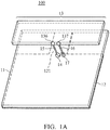
- FIG. 1A is a pictorial drawing illustrating a mobile communication device 100 according to an embodiment of the invention.
- the mobile communication device 100 comprises a system circuit board 11 and an antenna 13.
- the system circuit board 11 comprises a system ground plane 12, which further comprises an additional ground 121 on the edge of the system ground plane 12.
- FIG. 1B is a pictorial drawing illustrating the antenna 13.
- the antenna 13 comprises: a first radiation element 131, a second radiation element 132, an antenna substrate 133, an antenna ground plane 134, and a transmission line 135.
- the antenna substrate 133 is substantially parallel to the system ground plane 12.
- the first and second radiation elements 131, 132 are disposed on the antenna substrate 133.
- the antenna ground plane 134 is disposed on the antenna substrate 133 and electrically connected to the system ground plane 12 via a shorting point 137, which may be substantially disposed between the first and second radiation elements 131, 132.
- the antenna ground plane 134 may substantially separate the first radiation element 131 from the second radiation element 132.
- the transmission line 135 is disposed on the antenna substrate 133 and electrically connected to the first and second radiation elements 131, 132 via first and second branches 135a, 135b of the transmission line 135, respectively.
- the transmission line 135 may have a feed point 136 for receiving signals, wherein the first and second branches 135a, 135b are both electrically connected to the feed point 136.
- the transmission line 135 may be a microstrip line.
- the first and second radiation elements 131, 132 and the transmission line 135 may be disposed on a first surface E1 of the antenna substrate 133, and the antenna ground plane 134 may be disposed on a second surface E2, opposite to the first surface E1, of the antenna substrate 133.
- first and second radiation elements 132, 132, the transmission line 135 and the antenna ground plane 134 may be all disposed on the same surface, such as the first or second surfaces E1, E2.
- the system ground plane 12, the antenna ground plane 134 and the transmission line 135 may be made of metal, such as copper or silver.
- the feed point 136 is electrically connected to a signal source 14 on the system circuit board 11 via a metal line 15.
- the shorting point 137 is electrically connected to the system ground plane 12 via a metal line 16, through a via-hole 17 of the system circuit board 11.
- FIG. 1C is a pictorial drawing illustrating the system circuit board 11 according to an embodiment of the invention.
- an area 31 on the additional ground 121 is the projection plane of the antenna ground plane 134.
- the additional ground 121 may overlap with the antenna ground plane 134 partially or completely.
- FIG. 1D is a pictorial drawing illustrating an antenna 23 according to an embodiment of the invention.
- the antenna 13 of the mobile communication device 100 may be replaced with the antenna 23.
- the transmission line 135 may comprise a circuit component 638.
- One of the first and second branches 135a, 135b of the transmission line 135 may comprise the circuit component 638.
- the circuit component 638 may be a resistor, an inductor, or a capacitor for impedance matching.
- the circuit component 638 is a chip inductor.
- FIG. IE is a pictorial drawing illustrating an antenna 33.
- the antenna ground plane 134 may not be disposed between the first and second radiation elements 131, 132. As shown in FIG. IE, the antenna ground plane 134 is disposed on one side of the antenna substrate 133, and the first and second radiation elements 131, 132 are both disposed on the other side of the antenna substrate 133. The location of the antenna ground plane 134 has no significant impact on performance of the mobile communication device 100.
- FIG. IF is a pictorial drawing illustrating an antenna 43 according to another embodiment of the invention. As shown in FIG.
- the antenna ground plane 134 may not be disposed between the first and second radiation elements 131, 132, and one of the first and second branches 135a, 135b of the transmission line 135 may comprise the circuit component 638.
- the antenna 13 of the mobile communication device 100 may be replaced with the antennas 23, 33 or 43, and if so, the mobile communication device 100 would still work normally.
- FIG. 2A is a side-view drawing illustrating the mobile communication device 100 according to an embodiment of the invention.
- a data transmission component 55 such as a USB connector, may be disposed between the additional ground 121 and the antenna ground plane 134 in order to reduce interference.
- the data transmission component 55 provides a data transmission interface between the mobile communication device 100 and an external device.
- FIG. 2B is a side-view drawing illustrating a mobile communication device 100 not to another embodiment of the invention. As shown in FIG. 2B , the data transmission component 55 may be disposed below the system ground plane 12 for reducing interference.
- FIG. 3 is a diagram 300 illustrating return loss of the antenna 13 according to an embodiment of the invention.
- FIG. 3 is utilized for illustrating return loss (unit: dB) over frequency (unit: MHz).
- the antenna 13 covers the first and second frequency bands 31, 32 according to the criterion set as 6dB.
- the first frequency band 31 is from about 704MHz to 960MHz
- the second frequency band 32 is from about 1710MHz to 2690MHz.
- the first frequency band 31 is from about 824MHz to 960MHz
- the second frequency band 32 is from about 1710MHz to 2170MHz.
- the antenna 23, 33 or 43 may also cover the same frequency bands as those of the antenna 13. Therefore, the antennas 13, 23, 33 or 43 of the mobile communication device 100 can be configured to cover the LTE700/GSM850/900 and GSM1800/1900/UMTS/LTE2300/2500 bands (LTE/WWAN 8 bands).
- FIG. 4A is a drawing illustrating a monopole antenna 401 according to an embodiment of the invention.
- FIG. 4B is a drawing illustrating a loop antenna 402 according to another embodiment of the invention.
- the monopole antenna 401 may bend, and the loop antenna 402 may be of other shapes, such as a rectangular shape or a triangular shape.
- Each of the first and second radiation elements 131, 132 may be the monopole antenna 401 or the loop antenna 402.
- the sizes of the elements in the mobile communication device 100 may be as follows: the system circuit board 11 is approximately 112mm by 60mm in area; the system ground plane 12 is approximately 100mm by 60mm in area and substantially a rectangular shape; the additional ground 121 is approximately 12mm by 10mm in area; the antenna ground plane 134 is approximately 12mm by 10mm in area and substantially a rectangular shape; and the metal lines 15, 16 are both approximately 5mm in length and 1mm in width. It is noted that the sizes of the elements in the above embodiment are not limited. A person of ordinary skill can adjust the sizes of the elements according to the frequency band and the dielectric coefficient of designs.
- FIG. 5A is a pictorial drawing illustrating an antenna device 500 not to an embodiment of the invention.
- the design of the antenna device 500 is consistent with the basic structure of the mobile communication device 100, as shown in FIG 1A .
- the antenna device 500 comprises a system circuit board 51 and an antenna component 53.
- the system circuit board 51 comprises a system ground plane 52, which may comprise an additional ground 521 on the edge of the system ground plane 52. It is noted that the antenna device 500 may merely include the system ground plane 52, without the system circuit board 51, and the antenna component 53.
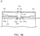
- FIG. 5B is a plan-view drawing illustrating the antenna device 500.
- the antenna component 53 comprises: a first radiation element 531, a second radiation element 532, an antenna substrate 533, an antenna ground plane 534, and a transmission line 535.
- the antenna substrate 533 is substantially parallel to the system ground plane 52.
- the first and second radiation elements 531, 532 are disposed on the antenna substrate 533 and electrically coupled to the system ground plane 52 via shorting vias S1, S2, respectively.
- the first radiation element 531 is electrically coupled to the system ground plane 52 through the antenna ground plane 534, wherein the shorting via S1 is electrically connected between the first radiation element 531 and the antenna ground plane 534.
- the second radiation element 532 is electrically coupled to the system ground plane 52 through the antenna ground plane 534, wherein the shorting via S2 is electrically connected between the second radiation element 532 and the antenna ground plane 534.
- the antenna ground plane 534 is disposed on the antenna substrate 533 and electrically connected to the system ground plane 52 via a shorting point 137, which may be substantially disposed between the first and second radiation elements 531, 532.
- the additional ground 521 may overlap with the antenna ground plane 534 partially or completely.
- the antenna ground plane 534 may substantially separate the first radiation element 531 from the second radiation element 532. It is noted that the antenna ground plane 534 may not be disposed between the first and second radiation elements 531, 532, as shown in FIG.
- the antenna ground plane 534 may be removed from the antenna component 53, and if so, the antenna device 500 would still work normally. Without the antenna ground plane 534, the first and second radiation elements 531, 532 may be directly and electrically connected to the system ground plane 52.
- the transmission line 535 is disposed on the antenna substrate 533 and comprises first and second branches 535a, 535b.
- the first branch 535a is close to the first radiation element 531 for mutual coupling and comprises a chip inductor 639, which has an inductance equal to about 15nH.
- the second branch 535b is close to the second radiation element 532 for mutual coupling.
- the transmission line 535 may have a feed point 136 for receiving signals, wherein the first and second branches 535a, 535b are both electrically connected to the feed point 136.
- the transmission line 535 may be a microstrip line.
- the system ground plane 52, the first and second radiation elements 531, 532, the antenna ground plane 534 and the transmission line 535 may be made of metal, such as copper or silver.
- the feed point 136 is electrically connected to a signal source 54 on the system circuit board 51 via a metal line.
- the shorting point 137 is electrically connected to the system ground plane 52 via another metal line.
- the Universal Serial Bus (USB) connector 555 may be disposed below the system ground plane 52, as shown in FIGS 2B , 5A . In another embodiment, the USB connector 555 may be disposed between the additional ground 521 and the antenna ground plane 534 in order to reduce interference, as shown in FIG. 2A .
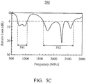
- FIG. 5C is a diagram 590 illustrating return loss of the antenna device 500.
- FIG. 5C is utilized for illustrating return loss (unit: dB) over frequency (unit: MHz).
- the antenna device 500 covers the first and second frequency bands 591, 592 according to the criterion set as 6dB.
- the first frequency band 591 is from about 704MHz to 960MHz
- the second frequency band 592 is from about 1710MHz to 2690MHz.
- the first frequency band 591 is from about 824MHz to 960MHz
- the second frequency band 592 is from about 1710MHz to 2170MHz.
- the first branch 535a and the first radiation element 531 are excited, and the second branch 535b and the second radiation element 532 are also excited, to form the first frequency band 591 together.
- the second branch 535b and the second radiation element 532 are excited to form the second frequency band 592.
- the sizes of the elements in the antenna device 500 are as follows.
- the system circuit board 51 has a dielectric constant equal to 4.3 (FR4 substrate) and of 0.8mm thickness.
- the antenna substrate 533 has a dielectric constant equal to 4.3 (FR4 substrate) and of 1mm thickness.
- the antenna ground plane 534 is approximately 60 mm 2 , e.g., 5mm by 12mm, in area.
- the additional ground 521 is approximately 108 mm 2 , e.g., 9mm by 12mm, in area.
- the first branch 535a is approximately 10mm in length, and the second branch 535b is approximately 26.5 mm in length.
- the total length of the first radiation element 531 is approximately 60.5 mm, and the total length of the second radiation element 532 is approximately 62mm. It is noted that the sizes of the elements in the above embodiment are not limited. A person of ordinary skill can adjust the sizes of the elements according to the frequency band and the dielectric constant.
- FIG. 6A is a pictorial drawing illustrating an antenna device 600 not to another embodiment of the invention.
- the design of the antenna device 600 is consistent with the basic structure of the mobile communication device 100, as shown in FIG 1A .
- the antenna device 600 comprises a system circuit board 61 and an antenna component 63.
- the system circuit board 61 comprises a system ground plane 62, which may comprise an additional ground 621 on the edge of the system ground plane 62. It is noted that the antenna device 600 may merely include the system ground plane 62, without the system circuit board 61, and the antenna component 63.
- FIG. 6B is a plan-view drawing illustrating the antenna device 600.
- the antenna component 63 comprises: a first radiation element 631, a second radiation element 632, an antenna substrate 633, an antenna ground plane 634, and a transmission line 635.
- the antenna substrate 633 is substantially parallel to the system ground plane 62.
- the first and second radiation elements 631, 632 are disposed on the antenna substrate 633 and electrically coupled to the system ground plane 62 via shorting vias S3, S4, respectively.
- the first radiation element 631 is electrically coupled to the system ground plane 62 through the antenna ground plane 634, wherein the shorting via S3 is electrically connected between the first radiation element 631 and the antenna ground plane 634.
- the second radiation element 632 is electrically connected to the system ground plane 62, wherein the shorting via S4 is electrically connected to the system ground plane 62 via a metal line.
- the antenna ground plane 634 is disposed on the antenna substrate 633 and electrically connected to the system ground plane 62 via a shorting point 137, which may be substantially disposed between the first and second radiation elements 631, 632.
- the additional ground 621 may overlap with the antenna ground plane 634 partially or completely.
- the antenna ground plane 634 may substantially separate the first radiation element 631 from the second radiation element 632. It is noted that the antenna ground plane 634 may not be disposed between the first and second radiation elements 631, 632, as shown in FIG. 1E or FIG. 1F .
- the antenna ground plane 634 may be removed from the antenna component 63, and if so, the antenna device 600 would still work normally. Without the antenna ground plane 634, the first radiation element 531 may be directly and electrically connected to the system ground plane 62.
- the transmission line 635 is disposed on the antenna substrate 633 and comprises first and second branches 635a, 635b.
- the first branch 635a is close to the first radiation element 631 for mutual coupling and comprises a chip inductor 639, which has an inductance equal to 15nH.
- the second branch 635b is not required to be close to the second radiation element 632.
- the transmission line 635 may have a feed point 136 for receiving signals, wherein the first and second branches 635a, 635b are both electrically connected to the feed point 136.
- the transmission line 635 may be a microstrip line.
- the system ground plane 62, the first and second radiation elements 631, 632, the antenna ground plane 634 and the transmission line 635 may be made of metal, such as copper or silver.
- the feed point 136 is electrically connected to a signal source 64 on the system circuit board 61 via a metal line.
- the shorting point 137 is electrically connected to the system ground plane 62 via another metal line.
- the USB connector 655 may be disposed below the system ground plane 62, as shown in FIGS 2B , 6A . In another embodiment, the USB connector 655 may be disposed between the additional ground 621 and the antenna ground plane 634 in order to reduce interference, as shown in FIG. 2A .
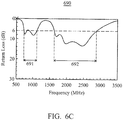
- FIG. 6C is a diagram 690 illustrating return loss of the antenna device 600.
- FIG. 6C is utilized for illustrating return loss (unit: dB) over frequency (unit: MHz).
- the antenna device 600 covers the first and second frequency bands 691, 692 according to the criterion set as 6dB.
- the first frequency band 691 is from about 704MHz to 960MHz
- the second frequency band 692 is from about 1710MHz to 2690MHz.
- the first frequency band 691 is from about 824MHz to 960MHz
- the second frequency band 692 is from about 1710MHz to 2170MHz.
- the first branch 635a and the first radiation element 631 are excited to form the first frequency band 691.
- the second branch 635b and the second radiation element 632 are excited to form the second frequency band 692.
- the sizes of the elements in the antenna device 600 are as follows.
- the system circuit board 61 has a dielectric constant equal to 4.3 (FR4 substrate) and of 0.8mm thickness.
- the antenna substrate 633 has a dielectric constant equal to 4.3 (FR4 substrate) and of 1mm thickness.
- the antenna ground plane 634 is approximately 60 mm 2 , e.g., 5mm by 12mm, in area.
- the additional ground 621 is approximately 120 mm 2 , e.g., 10mm by 12mm, in area.
- the first branch 635a is approximately 17mm in length, and the second branch 635b is approximately 18mm in length.
- the total length of the first radiation element 631 is approximately 65 mm, and the total length of the second radiation element 632 is approximately 22mm. It is noted that the sizes of the elements in the above embodiment are not limited. A person of ordinary skill can adjust the sizes of the elements according to the frequency band and the dielectric constant.
- the invention provides mobile communication devices and antenna devices that can cover 8 frequency bands of LTE/WWAN of 4G communication systems.
- the mobile communication devices and antenna devices are further configured to accommodate a data transmission component, such as a USB connector. Because of the shield of the system ground plane (including the additional ground) or the antenna ground plane, the data transmission component has little impact on the mobile communication devices or the antenna devices, resulting in little signal interference. Therefore, the mobile communication devices and the antenna devices of the invention can have well HAC and SAR values.
- the antenna of the mobile communication device covers a first frequency band from 824MHz to 960MHz substantially and a second frequency band from 1710MHz to 2170MHz substantially.
- the antenna of the mobile communication device covers a first frequency band from 704MHz to 960MHz substantially and a second frequency band from 1710MHz to 2690MHz substantially.
- the first frequency band of the antenna device is from 824MHz to 960MHz substantially and the second frequency band of the antenna device is from 1710MHz to 2170MHz substantially.
- the first frequency band of the antenna device is from 704MHz to 960MHz substantially and the second frequency band of the antenna device is from 1710MHz to 2690MHz substantially.
Landscapes
- Engineering & Computer Science (AREA)
- Computer Networks & Wireless Communication (AREA)
- Details Of Aerials (AREA)
- Support Of Aerials (AREA)
Claims (6)
- Un dispositif de communication mobile, comprenant:une carte de circuit système (11), comprenant un plan de masse de système (12); etune antenne (13), comprenant:un substrat d'antenne (133), sensiblement parallèle au plan de masse du système (12);un premier élément radiant (131), disposé sur le substrat d'antenne;un deuxième élément radiant (132), disposé sur le substrat d'antenne;un plan de masse d'antenne (134), disposé sur le substrat d'antenne, et couplé au plan de masse du système; etune ligne de transmission (135), disposée sur le substrat d'antenne, couplée aux premier et second éléments radiants, et ayant un point d'alimentation (136) ;le plan de masse du système (12) comprenant une masse supplémentaire (121) qui chevauche partiellement ou complètement le plan de masse de l'antenne (134) ;dans lequel le substrat d'antenne (133) est substantiellement parallèle et espacé de la carte de circuit système (11),caractérisé en ce quela ligne de transmission a une première branche (135a) connectée au premier élément radiant (131), et une seconde branche (135b) connectée au second élément radiant (132), dans lequel la première branche et la seconde branches sont toutes les deux connectées au point d'alimentation (136),dans lequel la première branche (135a) comporte une inductance de circuit (638) ;dans lequel un composant de transmission de données (55) est disposé entre la terre additionnelle et le plan de terre d'antenne, et le composant de transmission de données fournit une interface de transmission de données entre le dispositif de communication mobile et un dispositif externe.
- Le dispositif de communication mobile tel que revendiqué dans la revendication 1 dans lequel le composant de transmission de données est un connecteur Bus Série Universel (USB).
- Le dispositif de communication mobile tel que revendiqué dans l'une quelconque des revendications précédentes, dans lequel le plan de masse d'antenne sépare sensiblement le premier élément radiant (131) du second élément radiant (132).
- Le dispositif de communication mobile tel que revendiqué dans l'une quelconque des revendications précédentes dans lequel la ligne de transmission est une ligne microruban.
- Le dispositif de communication mobile tel que revendiqué dans l'une quelconque des revendications précédentes, dans lequel le premier élément radiant et/ou le second élément radiant est une antenne en boucle ou une antenne monopôle.
- Le dispositif de communication mobile tel que revendiqué dans l'une quelconque des revendications précédentes, dans lequel le point d'alimentation est couplé à une source de signal sur la carte de circuit du système.
Applications Claiming Priority (1)
| Application Number | Priority Date | Filing Date | Title |
|---|---|---|---|
| US13/182,277 US9077077B2 (en) | 2011-07-13 | 2011-07-13 | Mobile communication device and antenna device |
Publications (2)
| Publication Number | Publication Date |
|---|---|
| EP2546922A1 EP2546922A1 (fr) | 2013-01-16 |
| EP2546922B1 true EP2546922B1 (fr) | 2018-09-12 |
Family
ID=44983442
Family Applications (1)
| Application Number | Title | Priority Date | Filing Date |
|---|---|---|---|
| EP11183951.0A Active EP2546922B1 (fr) | 2011-07-13 | 2011-10-05 | Dispositif de communication mobile et dispositif d'antenne |
Country Status (4)
| Country | Link |
|---|---|
| US (1) | US9077077B2 (fr) |
| EP (1) | EP2546922B1 (fr) |
| CN (1) | CN102881997B (fr) |
| TW (1) | TWI481112B (fr) |
Families Citing this family (27)
| Publication number | Priority date | Publication date | Assignee | Title |
|---|---|---|---|---|
| US8922448B2 (en) * | 2012-09-26 | 2014-12-30 | Mediatek Singapore Pte. Ltd. | Communication device and antennas with high isolation characteristics |
| US9590303B2 (en) | 2013-01-29 | 2017-03-07 | Asustek Computer Inc. | Antenna |
| US9257750B2 (en) | 2013-05-15 | 2016-02-09 | Apple Inc. | Electronic device with multiband antenna |
| CN104218315B (zh) * | 2013-06-04 | 2018-07-27 | 深圳富泰宏精密工业有限公司 | 天线结构及应用该天线结构的无线通信装置 |
| US9515384B2 (en) | 2013-09-03 | 2016-12-06 | Mediatek Inc. | Apparatus and method for setting antenna resonant mode of multi-port antenna structure |
| CN103579746B (zh) * | 2013-09-30 | 2016-06-08 | 苏州佳世达电通有限公司 | 天线装置及应用其的通讯装置 |
| CN103715497B (zh) * | 2013-12-13 | 2016-08-17 | 惠州硕贝德无线科技股份有限公司 | 一种小型化lte/wwan天线 |
| CN104716416A (zh) * | 2013-12-13 | 2015-06-17 | 展讯通信(上海)有限公司 | 一种天线装置 |
| KR102208966B1 (ko) * | 2014-10-23 | 2021-01-28 | 삼성전자주식회사 | 근거리 통신용 칩 안테나 및 그 제조방법 |
| USD754108S1 (en) * | 2014-10-29 | 2016-04-19 | Airgain, Inc. | Antenna |
| USD798846S1 (en) * | 2014-11-17 | 2017-10-03 | Airgain Incorporated | Antenna assembly |
| USD804457S1 (en) * | 2014-12-31 | 2017-12-05 | Airgain Incorporated | Antenna assembly |
| USD804458S1 (en) * | 2014-12-31 | 2017-12-05 | Airgain Incorporated | Antenna |
| US9780452B2 (en) * | 2015-01-05 | 2017-10-03 | Sony Corporation | Communication terminal |
| TWI550390B (zh) | 2015-07-09 | 2016-09-21 | 廣達電腦股份有限公司 | 可變形行動裝置 |
| USD813851S1 (en) * | 2015-07-30 | 2018-03-27 | Airgain Incorporated | Antenna |
| KR102490416B1 (ko) | 2016-01-21 | 2023-01-19 | 삼성전자주식회사 | 안테나 장치 및 그를 구비하는 전자 장치 |
| EP3353852B1 (fr) * | 2016-02-19 | 2021-12-29 | Hewlett-Packard Development Company, L.P. | Parties d'antenne |
| TWI633705B (zh) * | 2016-06-13 | 2018-08-21 | 宏碁股份有限公司 | 行動裝置 |
| USD803197S1 (en) * | 2016-10-11 | 2017-11-21 | Airgain Incorporated | Set of antennas |
| CN106684558B (zh) * | 2016-11-02 | 2023-12-29 | 上海捷士太通讯技术有限公司 | 一种自带匹配电路的天线 |
| USD807333S1 (en) * | 2016-11-06 | 2018-01-09 | Airgain Incorporated | Set of antennas |
| US10944151B2 (en) * | 2017-02-24 | 2021-03-09 | Chiun Mai Communication Systems, Inc. | Antenna structure and wireless communication device using same |
| TWI668913B (zh) * | 2018-03-21 | 2019-08-11 | 啟碁科技股份有限公司 | 天線結構 |
| CN210757707U (zh) * | 2019-06-21 | 2020-06-16 | 深圳岱仕科技有限公司 | 机械外骨骼及外骨骼设备 |
| US11862838B2 (en) * | 2020-04-17 | 2024-01-02 | Apple Inc. | Electronic devices having wideband antennas |
| US11417951B2 (en) | 2020-09-01 | 2022-08-16 | Apple Inc. | Electronic devices having antennas that radiate through three-dimensionally curved cover layers |
Citations (1)
| Publication number | Priority date | Publication date | Assignee | Title |
|---|---|---|---|---|
| US20100164835A1 (en) * | 2008-12-30 | 2010-07-01 | Hon Hai Precision Ind. Co., Ltd. | Electrical connector assembly with antenna function |
Family Cites Families (23)
| Publication number | Priority date | Publication date | Assignee | Title |
|---|---|---|---|---|
| JP3319268B2 (ja) | 1996-02-13 | 2002-08-26 | 株式会社村田製作所 | 表面実装型アンテナおよびこれを用いた通信機 |
| EP1126522A1 (fr) * | 2000-02-18 | 2001-08-22 | Alcatel | Circuit intégré empaqueté avec antenne radiofréquence |
| US6466170B2 (en) | 2001-03-28 | 2002-10-15 | Motorola, Inc. | Internal multi-band antennas for mobile communications |
| US6552686B2 (en) | 2001-09-14 | 2003-04-22 | Nokia Corporation | Internal multi-band antenna with improved radiation efficiency |
| US6842141B2 (en) * | 2002-02-08 | 2005-01-11 | Virginia Tech Inellectual Properties Inc. | Fourpoint antenna |
| US6867736B2 (en) * | 2002-11-08 | 2005-03-15 | Motorola, Inc. | Multi-band antennas |
| JP2005150937A (ja) * | 2003-11-12 | 2005-06-09 | Murata Mfg Co Ltd | アンテナ構造およびそれを備えた通信機 |
| JP4063833B2 (ja) | 2004-06-14 | 2008-03-19 | Necアクセステクニカ株式会社 | アンテナ装置及び携帯無線端末 |
| US20070035452A1 (en) * | 2005-08-09 | 2007-02-15 | Hsin-Lung Lin | Patch antenna having a universal serial bus (USB) connection port |
| TWI258891B (en) | 2005-09-22 | 2006-07-21 | Ind Tech Res Inst | Mobile phone antenna |
| US7656353B2 (en) | 2005-11-29 | 2010-02-02 | Research In Motion Limited | Mobile wireless communications device comprising a satellite positioning system antenna with active and passive elements and related methods |
| US7312756B2 (en) * | 2006-01-09 | 2007-12-25 | Wistron Neweb Corp. | Antenna |
| US7659853B2 (en) | 2006-09-25 | 2010-02-09 | Htc Corporation | Miniaturized multi-band antenna |
| KR100809913B1 (ko) | 2006-09-25 | 2008-03-06 | 삼성전자주식회사 | 휴대용 단말기의 내장형 안테나 장치 |
| US7688267B2 (en) | 2006-11-06 | 2010-03-30 | Apple Inc. | Broadband antenna with coupled feed for handheld electronic devices |
| US7825863B2 (en) * | 2006-11-16 | 2010-11-02 | Galtronics Ltd. | Compact antenna |
| US20080180326A1 (en) * | 2007-01-30 | 2008-07-31 | Alpha Networks Inc. | Pendulum-shaped microstrip antenna structure |
| JP4389275B2 (ja) | 2007-08-24 | 2009-12-24 | 株式会社村田製作所 | アンテナ装置及び無線通信機 |
| CN101499562A (zh) * | 2008-02-03 | 2009-08-05 | 和硕联合科技股份有限公司 | 双馈入平板天线 |
| US8035566B2 (en) | 2009-05-06 | 2011-10-11 | Cheng Uei Precision Industry Co., Ltd. | Multi-band antenna |
| CN101640306B (zh) * | 2009-09-07 | 2013-03-06 | 清华大学 | 一种用于移动终端的天线结构 |
| TWI419405B (zh) * | 2009-10-08 | 2013-12-11 | Acer Inc | 行動通訊裝置及其天線 |
| TWI423521B (zh) * | 2009-10-26 | 2014-01-11 | Acer Inc | 多頻行動通訊裝置及其天線 |
-
2011
- 2011-07-13 US US13/182,277 patent/US9077077B2/en active Active
- 2011-09-28 TW TW100134933A patent/TWI481112B/zh active
- 2011-10-05 EP EP11183951.0A patent/EP2546922B1/fr active Active
- 2011-11-30 CN CN201110391474.XA patent/CN102881997B/zh active Active
Patent Citations (1)
| Publication number | Priority date | Publication date | Assignee | Title |
|---|---|---|---|---|
| US20100164835A1 (en) * | 2008-12-30 | 2010-07-01 | Hon Hai Precision Ind. Co., Ltd. | Electrical connector assembly with antenna function |
Also Published As
| Publication number | Publication date |
|---|---|
| US9077077B2 (en) | 2015-07-07 |
| TWI481112B (zh) | 2015-04-11 |
| TW201304273A (zh) | 2013-01-16 |
| EP2546922A1 (fr) | 2013-01-16 |
| CN102881997A (zh) | 2013-01-16 |
| CN102881997B (zh) | 2015-03-25 |
| US20130016013A1 (en) | 2013-01-17 |
Similar Documents
| Publication | Publication Date | Title |
|---|---|---|
| EP2546922B1 (fr) | Dispositif de communication mobile et dispositif d'antenne | |
| TWI658645B (zh) | 天線結構及具有該天線結構之無線通訊裝置 | |
| EP2083472B1 (fr) | Isolation d'antenne pour dispositifs électroniques portables | |
| US6943733B2 (en) | Multi-band planar inverted-F antennas including floating parasitic elements and wireless terminals incorporating the same | |
| EP2356719B1 (fr) | Ensemble antenne repliée extraplate pour dispositifs de communication portables | |
| TWI644479B (zh) | 多天線裝置 | |
| US20040145527A1 (en) | Planar antenna structure and radio device | |
| EP1755191B1 (fr) | Dispositif d'antenne pour terminal de communication cellulaire | |
| KR20180030902A (ko) | 웨어러블 무선 장치의 결합 다중 대역 안테나 | |
| US20150244063A1 (en) | Apparatus for wireless communication | |
| US6563466B2 (en) | Multi-frequency band inverted-F antennas with coupled branches and wireless communicators incorporating same | |
| CA2377921A1 (fr) | Antenne a deux voies integrable | |
| TWI646731B (zh) | 行動電子裝置 | |
| US20110128190A1 (en) | Wireless communication terminal with a split multi-band antenna having a single rf feed node | |
| EP2677596B1 (fr) | Dispositif de communication et système d'antenne correspondante | |
| US10622704B2 (en) | Embedded antenna | |
| EP1798808B1 (fr) | Terminal mobile à plusieurs antennes | |
| US8947314B2 (en) | Mobile communication device and built-in antenna integrated with a ground portion thereof | |
| TWI784626B (zh) | 支援寬頻操作之行動裝置 | |
| US20020123312A1 (en) | Antenna systems including internal planar inverted-F Antenna coupled with external radiating element and wireless communicators incorporating same | |
| CN101385191B (zh) | 一种天线布置 | |
| CN113078444A (zh) | 天线结构及具有该天线结构的无线通信装置 | |
| CN120749397A (zh) | 一种天线组件及电子设备 | |
| EP2493012B1 (fr) | Antenne de taille compacte fonctionnant dans des bandes de fréquence LTE | |
| KR100830568B1 (ko) | 셀룰러 통신 단말기용 안테나 장치 |
Legal Events
| Date | Code | Title | Description |
|---|---|---|---|
| PUAI | Public reference made under article 153(3) epc to a published international application that has entered the european phase |
Free format text: ORIGINAL CODE: 0009012 |
|
| AK | Designated contracting states |
Kind code of ref document: A1 Designated state(s): AL AT BE BG CH CY CZ DE DK EE ES FI FR GB GR HR HU IE IS IT LI LT LU LV MC MK MT NL NO PL PT RO RS SE SI SK SM TR |
|
| AX | Request for extension of the european patent |
Extension state: BA ME |
|
| 17P | Request for examination filed |
Effective date: 20120525 |
|
| 17Q | First examination report despatched |
Effective date: 20150812 |
|
| STAA | Information on the status of an ep patent application or granted ep patent |
Free format text: STATUS: EXAMINATION IS IN PROGRESS |
|
| GRAP | Despatch of communication of intention to grant a patent |
Free format text: ORIGINAL CODE: EPIDOSNIGR1 |
|
| STAA | Information on the status of an ep patent application or granted ep patent |
Free format text: STATUS: GRANT OF PATENT IS INTENDED |
|
| INTG | Intention to grant announced |
Effective date: 20180529 |
|
| GRAS | Grant fee paid |
Free format text: ORIGINAL CODE: EPIDOSNIGR3 |
|
| GRAA | (expected) grant |
Free format text: ORIGINAL CODE: 0009210 |
|
| STAA | Information on the status of an ep patent application or granted ep patent |
Free format text: STATUS: THE PATENT HAS BEEN GRANTED |
|
| AK | Designated contracting states |
Kind code of ref document: B1 Designated state(s): AL AT BE BG CH CY CZ DE DK EE ES FI FR GB GR HR HU IE IS IT LI LT LU LV MC MK MT NL NO PL PT RO RS SE SI SK SM TR |
|
| REG | Reference to a national code |
Ref country code: GB Ref legal event code: FG4D |
|
| REG | Reference to a national code |
Ref country code: CH Ref legal event code: EP |
|
| REG | Reference to a national code |
Ref country code: IE Ref legal event code: FG4D |
|
| REG | Reference to a national code |
Ref country code: DE Ref legal event code: R096 Ref document number: 602011051937 Country of ref document: DE |
|
| REG | Reference to a national code |
Ref country code: AT Ref legal event code: REF Ref document number: 1041670 Country of ref document: AT Kind code of ref document: T Effective date: 20181015 |
|
| REG | Reference to a national code |
Ref country code: NL Ref legal event code: MP Effective date: 20180912 |
|
| REG | Reference to a national code |
Ref country code: LT Ref legal event code: MG4D |
|
| PG25 | Lapsed in a contracting state [announced via postgrant information from national office to epo] |
Ref country code: FI Free format text: LAPSE BECAUSE OF FAILURE TO SUBMIT A TRANSLATION OF THE DESCRIPTION OR TO PAY THE FEE WITHIN THE PRESCRIBED TIME-LIMIT Effective date: 20180912 Ref country code: LT Free format text: LAPSE BECAUSE OF FAILURE TO SUBMIT A TRANSLATION OF THE DESCRIPTION OR TO PAY THE FEE WITHIN THE PRESCRIBED TIME-LIMIT Effective date: 20180912 Ref country code: BG Free format text: LAPSE BECAUSE OF FAILURE TO SUBMIT A TRANSLATION OF THE DESCRIPTION OR TO PAY THE FEE WITHIN THE PRESCRIBED TIME-LIMIT Effective date: 20181212 Ref country code: GR Free format text: LAPSE BECAUSE OF FAILURE TO SUBMIT A TRANSLATION OF THE DESCRIPTION OR TO PAY THE FEE WITHIN THE PRESCRIBED TIME-LIMIT Effective date: 20181213 Ref country code: NO Free format text: LAPSE BECAUSE OF FAILURE TO SUBMIT A TRANSLATION OF THE DESCRIPTION OR TO PAY THE FEE WITHIN THE PRESCRIBED TIME-LIMIT Effective date: 20181212 Ref country code: RS Free format text: LAPSE BECAUSE OF FAILURE TO SUBMIT A TRANSLATION OF THE DESCRIPTION OR TO PAY THE FEE WITHIN THE PRESCRIBED TIME-LIMIT Effective date: 20180912 Ref country code: SE Free format text: LAPSE BECAUSE OF FAILURE TO SUBMIT A TRANSLATION OF THE DESCRIPTION OR TO PAY THE FEE WITHIN THE PRESCRIBED TIME-LIMIT Effective date: 20180912 |
|
| PG25 | Lapsed in a contracting state [announced via postgrant information from national office to epo] |
Ref country code: LV Free format text: LAPSE BECAUSE OF FAILURE TO SUBMIT A TRANSLATION OF THE DESCRIPTION OR TO PAY THE FEE WITHIN THE PRESCRIBED TIME-LIMIT Effective date: 20180912 Ref country code: AL Free format text: LAPSE BECAUSE OF FAILURE TO SUBMIT A TRANSLATION OF THE DESCRIPTION OR TO PAY THE FEE WITHIN THE PRESCRIBED TIME-LIMIT Effective date: 20180912 Ref country code: HR Free format text: LAPSE BECAUSE OF FAILURE TO SUBMIT A TRANSLATION OF THE DESCRIPTION OR TO PAY THE FEE WITHIN THE PRESCRIBED TIME-LIMIT Effective date: 20180912 |
|
| REG | Reference to a national code |
Ref country code: AT Ref legal event code: MK05 Ref document number: 1041670 Country of ref document: AT Kind code of ref document: T Effective date: 20180912 |
|
| PG25 | Lapsed in a contracting state [announced via postgrant information from national office to epo] |
Ref country code: ES Free format text: LAPSE BECAUSE OF FAILURE TO SUBMIT A TRANSLATION OF THE DESCRIPTION OR TO PAY THE FEE WITHIN THE PRESCRIBED TIME-LIMIT Effective date: 20180912 Ref country code: IS Free format text: LAPSE BECAUSE OF FAILURE TO SUBMIT A TRANSLATION OF THE DESCRIPTION OR TO PAY THE FEE WITHIN THE PRESCRIBED TIME-LIMIT Effective date: 20190112 Ref country code: AT Free format text: LAPSE BECAUSE OF FAILURE TO SUBMIT A TRANSLATION OF THE DESCRIPTION OR TO PAY THE FEE WITHIN THE PRESCRIBED TIME-LIMIT Effective date: 20180912 Ref country code: EE Free format text: LAPSE BECAUSE OF FAILURE TO SUBMIT A TRANSLATION OF THE DESCRIPTION OR TO PAY THE FEE WITHIN THE PRESCRIBED TIME-LIMIT Effective date: 20180912 Ref country code: PL Free format text: LAPSE BECAUSE OF FAILURE TO SUBMIT A TRANSLATION OF THE DESCRIPTION OR TO PAY THE FEE WITHIN THE PRESCRIBED TIME-LIMIT Effective date: 20180912 Ref country code: IT Free format text: LAPSE BECAUSE OF FAILURE TO SUBMIT A TRANSLATION OF THE DESCRIPTION OR TO PAY THE FEE WITHIN THE PRESCRIBED TIME-LIMIT Effective date: 20180912 Ref country code: NL Free format text: LAPSE BECAUSE OF FAILURE TO SUBMIT A TRANSLATION OF THE DESCRIPTION OR TO PAY THE FEE WITHIN THE PRESCRIBED TIME-LIMIT Effective date: 20180912 Ref country code: RO Free format text: LAPSE BECAUSE OF FAILURE TO SUBMIT A TRANSLATION OF THE DESCRIPTION OR TO PAY THE FEE WITHIN THE PRESCRIBED TIME-LIMIT Effective date: 20180912 Ref country code: CZ Free format text: LAPSE BECAUSE OF FAILURE TO SUBMIT A TRANSLATION OF THE DESCRIPTION OR TO PAY THE FEE WITHIN THE PRESCRIBED TIME-LIMIT Effective date: 20180912 |
|
| PG25 | Lapsed in a contracting state [announced via postgrant information from national office to epo] |
Ref country code: PT Free format text: LAPSE BECAUSE OF FAILURE TO SUBMIT A TRANSLATION OF THE DESCRIPTION OR TO PAY THE FEE WITHIN THE PRESCRIBED TIME-LIMIT Effective date: 20190112 Ref country code: SM Free format text: LAPSE BECAUSE OF FAILURE TO SUBMIT A TRANSLATION OF THE DESCRIPTION OR TO PAY THE FEE WITHIN THE PRESCRIBED TIME-LIMIT Effective date: 20180912 Ref country code: SK Free format text: LAPSE BECAUSE OF FAILURE TO SUBMIT A TRANSLATION OF THE DESCRIPTION OR TO PAY THE FEE WITHIN THE PRESCRIBED TIME-LIMIT Effective date: 20180912 |
|
| REG | Reference to a national code |
Ref country code: CH Ref legal event code: PL |
|
| REG | Reference to a national code |
Ref country code: DE Ref legal event code: R097 Ref document number: 602011051937 Country of ref document: DE |
|
| REG | Reference to a national code |
Ref country code: BE Ref legal event code: MM Effective date: 20181031 |
|
| PG25 | Lapsed in a contracting state [announced via postgrant information from national office to epo] |
Ref country code: LU Free format text: LAPSE BECAUSE OF NON-PAYMENT OF DUE FEES Effective date: 20181005 |
|
| PLBE | No opposition filed within time limit |
Free format text: ORIGINAL CODE: 0009261 |
|
| STAA | Information on the status of an ep patent application or granted ep patent |
Free format text: STATUS: NO OPPOSITION FILED WITHIN TIME LIMIT |
|
| REG | Reference to a national code |
Ref country code: IE Ref legal event code: MM4A |
|
| PG25 | Lapsed in a contracting state [announced via postgrant information from national office to epo] |
Ref country code: MC Free format text: LAPSE BECAUSE OF FAILURE TO SUBMIT A TRANSLATION OF THE DESCRIPTION OR TO PAY THE FEE WITHIN THE PRESCRIBED TIME-LIMIT Effective date: 20180912 Ref country code: DK Free format text: LAPSE BECAUSE OF FAILURE TO SUBMIT A TRANSLATION OF THE DESCRIPTION OR TO PAY THE FEE WITHIN THE PRESCRIBED TIME-LIMIT Effective date: 20180912 |
|
| 26N | No opposition filed |
Effective date: 20190613 |
|
| PG25 | Lapsed in a contracting state [announced via postgrant information from national office to epo] |
Ref country code: LI Free format text: LAPSE BECAUSE OF NON-PAYMENT OF DUE FEES Effective date: 20181031 Ref country code: CH Free format text: LAPSE BECAUSE OF NON-PAYMENT OF DUE FEES Effective date: 20181031 Ref country code: BE Free format text: LAPSE BECAUSE OF NON-PAYMENT OF DUE FEES Effective date: 20181031 Ref country code: SI Free format text: LAPSE BECAUSE OF FAILURE TO SUBMIT A TRANSLATION OF THE DESCRIPTION OR TO PAY THE FEE WITHIN THE PRESCRIBED TIME-LIMIT Effective date: 20180912 |
|
| PG25 | Lapsed in a contracting state [announced via postgrant information from national office to epo] |
Ref country code: IE Free format text: LAPSE BECAUSE OF NON-PAYMENT OF DUE FEES Effective date: 20181005 Ref country code: FR Free format text: LAPSE BECAUSE OF NON-PAYMENT OF DUE FEES Effective date: 20181112 |
|
| PG25 | Lapsed in a contracting state [announced via postgrant information from national office to epo] |
Ref country code: MT Free format text: LAPSE BECAUSE OF NON-PAYMENT OF DUE FEES Effective date: 20181005 |
|
| PG25 | Lapsed in a contracting state [announced via postgrant information from national office to epo] |
Ref country code: TR Free format text: LAPSE BECAUSE OF FAILURE TO SUBMIT A TRANSLATION OF THE DESCRIPTION OR TO PAY THE FEE WITHIN THE PRESCRIBED TIME-LIMIT Effective date: 20180912 |
|
| PG25 | Lapsed in a contracting state [announced via postgrant information from national office to epo] |
Ref country code: MK Free format text: LAPSE BECAUSE OF NON-PAYMENT OF DUE FEES Effective date: 20180912 Ref country code: HU Free format text: LAPSE BECAUSE OF FAILURE TO SUBMIT A TRANSLATION OF THE DESCRIPTION OR TO PAY THE FEE WITHIN THE PRESCRIBED TIME-LIMIT; INVALID AB INITIO Effective date: 20111005 Ref country code: CY Free format text: LAPSE BECAUSE OF FAILURE TO SUBMIT A TRANSLATION OF THE DESCRIPTION OR TO PAY THE FEE WITHIN THE PRESCRIBED TIME-LIMIT Effective date: 20180912 |
|
| PGFP | Annual fee paid to national office [announced via postgrant information from national office to epo] |
Ref country code: GB Payment date: 20250814 Year of fee payment: 15 |
|
| PGFP | Annual fee paid to national office [announced via postgrant information from national office to epo] |
Ref country code: DE Payment date: 20250813 Year of fee payment: 15 |