EP2546986A2 - Geschachtelte Verbunddiode - Google Patents
Geschachtelte Verbunddiode Download PDFInfo
- Publication number
- EP2546986A2 EP2546986A2 EP12175466A EP12175466A EP2546986A2 EP 2546986 A2 EP2546986 A2 EP 2546986A2 EP 12175466 A EP12175466 A EP 12175466A EP 12175466 A EP12175466 A EP 12175466A EP 2546986 A2 EP2546986 A2 EP 2546986A2
- Authority
- EP
- European Patent Office
- Prior art keywords
- diode
- composite
- transistor
- nested
- primary
- Prior art date
- Legal status (The legal status is an assumption and is not a legal conclusion. Google has not performed a legal analysis and makes no representation as to the accuracy of the status listed.)
- Withdrawn
Links
Images


Classifications
-
- H—ELECTRICITY
- H03—ELECTRONIC CIRCUITRY
- H03K—PULSE TECHNIQUE
- H03K17/00—Electronic switching or gating, i.e. not by contact-making and –breaking
- H03K17/30—Modifications for providing a predetermined threshold before switching
- H03K17/302—Modifications for providing a predetermined threshold before switching in field-effect transistor switches
-
- H—ELECTRICITY
- H03—ELECTRONIC CIRCUITRY
- H03K—PULSE TECHNIQUE
- H03K17/00—Electronic switching or gating, i.e. not by contact-making and –breaking
- H03K17/51—Electronic switching or gating, i.e. not by contact-making and –breaking characterised by the components used
- H03K17/56—Electronic switching or gating, i.e. not by contact-making and –breaking characterised by the components used by the use, as active elements, of semiconductor devices
- H03K17/567—Circuits characterised by the use of more than one type of semiconductor device, e.g. BIMOS, composite devices such as IGBT
-
- H—ELECTRICITY
- H03—ELECTRONIC CIRCUITRY
- H03K—PULSE TECHNIQUE
- H03K17/00—Electronic switching or gating, i.e. not by contact-making and –breaking
- H03K17/51—Electronic switching or gating, i.e. not by contact-making and –breaking characterised by the components used
- H03K17/74—Electronic switching or gating, i.e. not by contact-making and –breaking characterised by the components used by the use, as active elements, of diodes
-
- H—ELECTRICITY
- H10—SEMICONDUCTOR DEVICES; ELECTRIC SOLID-STATE DEVICES NOT OTHERWISE PROVIDED FOR
- H10D—INORGANIC ELECTRIC SEMICONDUCTOR DEVICES
- H10D84/00—Integrated devices formed in or on semiconductor substrates that comprise only semiconducting layers, e.g. on Si wafers or on GaAs-on-Si wafers
- H10D84/01—Manufacture or treatment
-
- H—ELECTRICITY
- H10—SEMICONDUCTOR DEVICES; ELECTRIC SOLID-STATE DEVICES NOT OTHERWISE PROVIDED FOR
- H10D—INORGANIC ELECTRIC SEMICONDUCTOR DEVICES
- H10D84/00—Integrated devices formed in or on semiconductor substrates that comprise only semiconducting layers, e.g. on Si wafers or on GaAs-on-Si wafers
- H10D84/80—Integrated devices formed in or on semiconductor substrates that comprise only semiconducting layers, e.g. on Si wafers or on GaAs-on-Si wafers characterised by the integration of at least one component covered by groups H10D12/00 or H10D30/00, e.g. integration of IGFETs
- H10D84/811—Combinations of field-effect devices and one or more diodes, capacitors or resistors
Definitions
- group III-V refers to a compound semiconductor that includes a group V element and at least one group III element.
- III-Nitride or III-N refers to a compound semiconductor that includes nitrogen (N) and at least one group III element including aluminum (Al), gallium (Ga), indium (In), and boron (B), and including but not limited to any of its alloys, such as aluminum gallium nitride (Al x Ga (1-x) N), indium gallium nitride (In y Ga (1-y) N), aluminum indium gallium nitride (Al x In y Ga (1-x-y) N), gallium arsenide phosphide nitride (GaAs a P b N (1-a-b) ), and aluminum indium gallium arsenide phosphide nitride (Al x In y Ga (1-x-y) As a P b N (1
- III-Nitride also refers generally to any polarity including but not limited to Ga-polar, N-polar, semi-polar or non-polar crystal orientations.
- a III-Nitride material may also include either the Wurtzitic, Zincblende or mixed polytypes, and may include single-crystal, monocrystalline, polycrystalline, or amorphous structures.
- group IV refers to a semiconductor that includes at least one group four element including silicon (Si), germanium (Ge), and carbon (C), and also includes compound semiconductors such as SiGe and SiC, for example.
- Group IV may also refer to a semiconductor material which consists of layers of group IV elements or doping of group IV elements to produce strained silicon or other strained group IV material.
- group IV based composite substrates may include silicon on insulstor (SOI), separation by implantation of oxygen (SIMOX) process substrates, and silicon on sapphire (SOS), for example.
- SOI silicon on insulstor
- SIMOX separation by implantation of oxygen
- SOS silicon on sapphire
- a group IV device may include devices formed using standard CMOS processing, but may also include NMOS and PMOS device processing.
- the terms “LV device,” “low voltage semiconductor device,” “low voltage diode,” and the like refer to a low voltage device with a typical breakdown voltage rating less than an “intermediate device,” as described below.
- the LV device can include any suitable semiconductor material that forms a diode. Suitable semiconductor materials include group IV semiconductor materials such as Si, strained silicon, SiGe, SiC, and group III-V materials including III-As, III-P, III-Nitride or any of their alloys.
- intermediate device refers to a device with a typical breakdown voltage greater than the LV device and less than a "primary device.”
- primary device refers to a device with a typical breakdown voltage greater than both the intermediate device and the LV device.
- group III-V field-effect transistors FETs
- HEMTs high mobility electron transistors
- III-Nitride FETs and III-Nitride HEMTs are often desirable for their high efficiency and high-voltage operation.
- group III-V transistors with other semiconductor devices, such as group IV diodes, to create high performance composite diodes.
- a depletion mode (normally ON) III-Nitride or other group III-V transistor can be cascoded with a low-voltage (LV) group IV diode, for example a silicon diode, to produce a relatively high voltage composite diode.
- LV low-voltage
- the performance of the composite diode can be limited by the on-state and voltage breakdown characteristics of the LV group IV diode used.
- the breakdown voltage for a given on-state resistance of the LV group IV diode may be insufficient to support the required pinch-off voltage required to maintain the group III-V transistor in a satisfactorily OFF condition.
- the present disclosure is directed to a nested composite diode, substantially as shown in and/or described in connection with at least one of the figures, and as set forth more completely in the claims.
- Group III-V semiconductors include III-Nitride materials formed of gallium nitride (GaN) and/or its alloys, such as aluminum gallium nitride (AlGaN), indium gallium nitride (InGaN), and aluminum indium gallium nitride (AlInGaN). These materials are semiconductor compounds that have a relatively wide, direct bandgap and strong piezoelectric polarizations, and can support high breakdown fields, high saturation velocities, and the creation of two-dimensional electron gases (2DEGs). As a result, III-Nitride materials such as GaN are used in many microelectronic applications such as depletion mode (e.g., normally ON) power field-effect transistors (FETs) and high electron mobility transistors (HEMTs).
- depletion mode e.g., normally ON
- FETs field-effect transistors
- HEMTs high electron mobility transistors
- a normally ON III-Nitride or other group III-V transistor can be cascoded with a low voltage (LV) diode to produce a relatively high voltage composite diode.
- LV low voltage
- the performance of the composite diode can be limited by the on-state and voltage breakdown characteristics of the LV diode used.
- the breakdown voltage for a given on-state resistance of the LV group IV diode may be insufficient to support the required pinch-off voltage required to maintain the group III-V primary transistor in a satisfactorily OFF condition.
- an intermediate III-V transistor may be used in a nested cascode configuration.
- the present application is directed to a nested composite diode capable of providing enhanced voltage breakdown resistance while providing advantages, such as fast switching speed, typically associated with an LV device.
- the nested composite diode includes a primary transistor coupled to a composite diode.
- the composite diode may including an LV diode cascoded with an intermediate transistor (for example a depletion mode or normally ON III-N transistor) having a breakdown voltage greater than that that of the LV diode and less than that of the primary transistor.
- the composite diode including the LV diode can be cascoded with the primary transistor.
- the cascoded combination of the composite diode with the primary transistor which may be a normally ON III-Nitride or other group III-V device, for example, can be implemented to produce a nested composite diode having an increased speed and breakdown voltage.
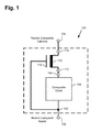
- Figure 1 shows one exemplary implementation of a nested composite diode including a primary transistor and a composite diode.
- nested composite diode 100 includes primary transistor 110 and composite diode 140 coupled to primary transistor 110.
- nested composite diode 100 has nested composite anode 102 and nested composite cathode 104.
- source 112, drain 114, and gate 116 of primary transistor 110, and composite anode 142 and composite cathode 144 of composite diode 140 are also shown in Figure 1 .
- Figure 2 shows a more detailed exemplary implementation of a composite diode suitable for use in a nested composite diode.
- composite diode 240 includes intermediate transistor 222 and LV diode 224 cascoded with intermediate transistor 222. Also shown in Figure 2 are composite anode 242 and composite cathode 244 of composite diode 240.
- Composite diode 240 having composite anode 242 and composite cathode 244 corresponds to composite diode 140 having composite anode 142 and composite cathode 144, in Figure 1 .
- LV diode 224 may be implemented as an LV group IV diode, such as a silicon diode having a breakdown voltage of approximately 10V or less, such as 3V, for example.
- Intermediate transistor 222 may be formed of III-N, and may be implemented as a HEMT or heterostructure FET (HFET), for example. According to one implementation, intermediate transistor 222 has a breakdown voltage greater than that of LV diode 224 and less than that of primary transistor 110, in Figure 1 . More specifically, the breakdown voltage of intermediate transistor 222 is typically greater than the largest pinch-off voltage required to turn primary transistor 110 OFF.
- HFET heterostructure FET
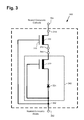
- FIG 3 shows an exemplary implementation of a nested composite diode including a primary transistor, and a composite diode corresponding generally to the implementation shown in Figure 2 .
- Nested composite diode 300 includes primary transistor 310 coupled to composite diode 340.
- composite diode 340 includes LV diode 324 cascoded with intermediate transistor 322.
- Also shown in Figure 3 are nested composite anode 302 and nested composite cathode 304 of nested composite diode 300, as well as source 312, drain 314, and gate 316 of primary transistor 310, and composite anode 342 and composite cathode 344 of composite diode 340.
- Nested composite diode 300 having nested composite anode 302 and nested composite cathode 304 corresponds to nested composite diode 100 having nested composite anode 102 and nested composite cathode 104, in Figure 1 , and may share any of the characteristics previously attributed to those corresponding features, above.
- composite diode 340 having composite anode 342 and composite cathode 344 corresponds to composite diode 240 having composite anode 242 and composite cathode 244, in Figure 2 , and may share any of the characteristics previously attributed to those corresponding features.
- Primary transistor 310 and composite diode 340 are coupled using a cascode configuration to produce nested composite diode 300, which according to the implementation shown in Figure 3 results in a composite two terminal device.
- nested composite diode 300 can function in effect as a diode having nested composite anode 302 provided by composite diode 340, and nested composite cathode 304 provided by primary transistor 310.
- composite cathode 344 of composite diode 340 is coupled to source 312 of primary transistor 310
- composite anode 342 of composite diode 340 provides nested composite anode 302 for nested composite diode 300.
- drain 314 of primary transistor 310 provides nested composite cathode 304 for nested composite diode 300
- gate 316 of primary transistor 310 is coupled to composite anode 342 of composite diode 340.
- the implementation shown in Figure 3 advantageously provides nested composite diode 300 having increased switching speed when compared to conventional high voltage diodes with comparable standoff capability. In some implementations, it may be advantageous to nest another high voltage or primary transistor with the nested composite diode shown in Figure 3 .
- An exemplary implementation of such a multi-nested composite diode is shown in Figure 4 .
- Multi-nested composite diode 401 includes higher voltage (HV+) primary transistor 411 coupled to nested composite diode 400.
- Nested composite diode 400 includes primary transistor 410 coupled to composite diode 440, and corresponds to nested composite diode 300 including primary transistor 310 coupled to composite diode 340, in Figure 3 .
- HV+ primary transistor refers to a primary transistor having a breakdown voltage equal to or greater than the breakdown voltage of primary transistor 410.
- HV+ primary transistor 411 and nested composite diode 400 are coupled using a cascode configuration to produce multi-nested composite diode 401. That is to say, nested composite cathode 404 of nested composite diode 400 is coupled to source 413 of HV+ primary transistor 411, and nested composite anode 402 of nested composite diode 400 provides multi-nested composite anode 403 for multi-nested composite diode 401.
- drain 415 of HV+ primary transistor 411 provides multi-nested composite cathode 405 for multi-nested composite diode 401, while gate 417 of HV+ primary transistor 411 is coupled to nested composite anode 402 of nested composite diode 400.
- the implementation shown in Figure 4 advantageously provides fast switching speed analogous to the implementation in Figure 3 , while producing a higher breakdown voltage.
- one possible solution for reducing package parasitics for nested composite diode 300 is through monolithic integration of primary transistor 310 and/or composite diode 340.
- two or more of primary transistor 310, intermediate transistor 322, and LV diode 324 may be monolithically integrated on a common composite semiconductor substrate designed to support both group IV and group III-V device fabrication.
- the present application discloses a nested composite diode having increased breakdown voltage.
- the implementations disclosed herein provide a nested composite diode having increased speed when compared to conventional high voltage devices.
- the addition of an intermediate switch allows the use of a low voltage diode which would not otherwise be capable of adequately maintaining the primary switch in an OFF state within a cascode configuration.
Landscapes
- Junction Field-Effect Transistors (AREA)
- Semiconductor Integrated Circuits (AREA)
- Metal-Oxide And Bipolar Metal-Oxide Semiconductor Integrated Circuits (AREA)
- Amplifiers (AREA)
Applications Claiming Priority (2)
| Application Number | Priority Date | Filing Date | Title |
|---|---|---|---|
| US201161506529P | 2011-07-11 | 2011-07-11 | |
| US13/542,453 US20130015501A1 (en) | 2011-07-11 | 2012-07-05 | Nested Composite Diode |
Publications (2)
| Publication Number | Publication Date |
|---|---|
| EP2546986A2 true EP2546986A2 (de) | 2013-01-16 |
| EP2546986A3 EP2546986A3 (de) | 2013-02-20 |
Family
ID=46799996
Family Applications (1)
| Application Number | Title | Priority Date | Filing Date |
|---|---|---|---|
| EP12175466A Withdrawn EP2546986A3 (de) | 2011-07-11 | 2012-07-06 | Geschachtelte Verbunddiode |
Country Status (3)
| Country | Link |
|---|---|
| US (1) | US20130015501A1 (de) |
| EP (1) | EP2546986A3 (de) |
| JP (1) | JP6008621B2 (de) |
Cited By (1)
| Publication number | Priority date | Publication date | Assignee | Title |
|---|---|---|---|---|
| US12408383B2 (en) | 2018-10-18 | 2025-09-02 | Semiconductor Energy Laboratory Co., Ltd. | Semiconductor device, semiconductor wafer, and electronic device |
Families Citing this family (8)
| Publication number | Priority date | Publication date | Assignee | Title |
|---|---|---|---|---|
| US9219058B2 (en) * | 2010-03-01 | 2015-12-22 | Infineon Technologies Americas Corp. | Efficient high voltage switching circuits and monolithic integration of same |
| US8981380B2 (en) * | 2010-03-01 | 2015-03-17 | International Rectifier Corporation | Monolithic integration of silicon and group III-V devices |
| US8988133B2 (en) | 2011-07-11 | 2015-03-24 | International Rectifier Corporation | Nested composite switch |
| US20150014784A1 (en) * | 2013-07-12 | 2015-01-15 | Delta Electronics, Inc. | Cascode switch device |
| US9741711B2 (en) * | 2014-10-28 | 2017-08-22 | Semiconductor Components Industries, Llc | Cascode semiconductor device structure and method therefor |
| CN105049821B (zh) * | 2015-08-04 | 2019-09-20 | 海信集团有限公司 | 一种色轮的自动调整方法及装置 |
| CN111404529B (zh) * | 2020-04-03 | 2023-04-25 | 电子科技大学 | 一种耗尽型GaN功率器件的分段直接栅驱动电路 |
| TWI857701B (zh) * | 2023-07-14 | 2024-10-01 | 即思創意股份有限公司 | 串疊二極體電路 |
Citations (1)
| Publication number | Priority date | Publication date | Assignee | Title |
|---|---|---|---|---|
| DE102004006537A1 (de) * | 2003-02-13 | 2004-08-26 | Denso Corp., Kariya | Durch ein Siliziumkarbidsubstrat gebildete Halbleitervorrichtung und Verfahren zur Herstellung derselben |
Family Cites Families (25)
| Publication number | Priority date | Publication date | Assignee | Title |
|---|---|---|---|---|
| JPS59223027A (ja) * | 1983-06-02 | 1984-12-14 | Oki Electric Ind Co Ltd | 半導体論理回路 |
| US5008565A (en) * | 1990-01-23 | 1991-04-16 | Triquint Semiconductor, Inc. | High-impedance FET circuit |
| US5422563A (en) * | 1993-07-22 | 1995-06-06 | Massachusetts Institute Of Technology | Bootstrapped current and voltage reference circuits utilizing an N-type negative resistance device |
| US6483369B1 (en) * | 2001-10-02 | 2002-11-19 | Technical Witts Inc. | Composite mosfet cascode switches for power converters |
| JP3847620B2 (ja) * | 2001-12-26 | 2006-11-22 | 日本テキサス・インスツルメンツ株式会社 | 駆動回路 |
| US6865093B2 (en) * | 2003-05-27 | 2005-03-08 | Power Integrations, Inc. | Electronic circuit control element with tap element |
| JP2005136948A (ja) * | 2003-10-08 | 2005-05-26 | Renesas Technology Corp | アンテナスイッチ回路 |
| US7276883B2 (en) * | 2004-08-12 | 2007-10-02 | International Rectifier Corporation | Self-driven synchronous rectified boost converter with inrush current protection using bidirectional normally on device |
| US7180762B2 (en) * | 2004-08-23 | 2007-02-20 | International Rectifier Corporation | Cascoded rectifier |
| JP4645313B2 (ja) * | 2005-06-14 | 2011-03-09 | 富士電機システムズ株式会社 | 半導体装置 |
| JP5358882B2 (ja) * | 2007-02-09 | 2013-12-04 | サンケン電気株式会社 | 整流素子を含む複合半導体装置 |
| JP2009182107A (ja) * | 2008-01-30 | 2009-08-13 | Furukawa Electric Co Ltd:The | 半導体装置 |
| US8957642B2 (en) * | 2008-05-06 | 2015-02-17 | International Rectifier Corporation | Enhancement mode III-nitride switch with increased efficiency and operating frequency |
| US9502973B2 (en) * | 2009-04-08 | 2016-11-22 | Infineon Technologies Americas Corp. | Buck converter with III-nitride switch for substantially increased input-to-output voltage ratio |
| US7915645B2 (en) * | 2009-05-28 | 2011-03-29 | International Rectifier Corporation | Monolithic vertically integrated composite group III-V and group IV semiconductor device and method for fabricating same |
| US8269259B2 (en) * | 2009-12-07 | 2012-09-18 | International Rectifier Corporation | Gated AlGaN/GaN heterojunction Schottky device |
| US8390395B2 (en) * | 2010-05-03 | 2013-03-05 | Raytheon Company | High power RF switch with active device size tapering |
| US8455948B2 (en) * | 2011-01-07 | 2013-06-04 | Infineon Technologies Austria Ag | Transistor arrangement with a first transistor and with a plurality of second transistors |
| US8963338B2 (en) * | 2011-03-02 | 2015-02-24 | International Rectifier Corporation | III-nitride transistor stacked with diode in a package |
| US9076853B2 (en) * | 2011-03-18 | 2015-07-07 | International Rectifie Corporation | High voltage rectifier and switching circuits |
| US20130175542A1 (en) * | 2011-04-11 | 2013-07-11 | International Rectifier Corporation | Group III-V and Group IV Composite Diode |
| US8853706B2 (en) * | 2011-05-04 | 2014-10-07 | International Rectifier Corporation | High voltage cascoded III-nitride rectifier package with stamped leadframe |
| US8853707B2 (en) * | 2011-05-04 | 2014-10-07 | International Rectifier Corporation | High voltage cascoded III-nitride rectifier package with etched leadframe |
| JP2014027253A (ja) * | 2012-06-22 | 2014-02-06 | Toshiba Corp | 整流回路 |
| JP2014158352A (ja) * | 2013-02-15 | 2014-08-28 | Toshiba Lighting & Technology Corp | 整流回路 |
-
2012
- 2012-07-05 US US13/542,453 patent/US20130015501A1/en not_active Abandoned
- 2012-07-06 JP JP2012152914A patent/JP6008621B2/ja not_active Expired - Fee Related
- 2012-07-06 EP EP12175466A patent/EP2546986A3/de not_active Withdrawn
Patent Citations (1)
| Publication number | Priority date | Publication date | Assignee | Title |
|---|---|---|---|---|
| DE102004006537A1 (de) * | 2003-02-13 | 2004-08-26 | Denso Corp., Kariya | Durch ein Siliziumkarbidsubstrat gebildete Halbleitervorrichtung und Verfahren zur Herstellung derselben |
Cited By (1)
| Publication number | Priority date | Publication date | Assignee | Title |
|---|---|---|---|---|
| US12408383B2 (en) | 2018-10-18 | 2025-09-02 | Semiconductor Energy Laboratory Co., Ltd. | Semiconductor device, semiconductor wafer, and electronic device |
Also Published As
| Publication number | Publication date |
|---|---|
| JP6008621B2 (ja) | 2016-10-19 |
| JP2013021329A (ja) | 2013-01-31 |
| EP2546986A3 (de) | 2013-02-20 |
| US20130015501A1 (en) | 2013-01-17 |
Similar Documents
| Publication | Publication Date | Title |
|---|---|---|
| EP2546986A2 (de) | Geschachtelte Verbunddiode | |
| US9041067B2 (en) | Integrated half-bridge circuit with low side and high side composite switches | |
| US9461034B2 (en) | Composite group III-V and group IV transistor having a switched substrate | |
| US9859882B2 (en) | High voltage composite semiconductor device with protection for a low voltage device | |
| US9310819B2 (en) | Power converter including integrated driver providing overcurrent protection | |
| US9406674B2 (en) | Integrated III-nitride D-mode HFET with cascoded pair half bridge | |
| US8988133B2 (en) | Nested composite switch | |
| US9349715B2 (en) | Depletion mode group III-V transistor with high voltage group IV enable switch | |
| US9087812B2 (en) | Composite semiconductor device with integrated diode | |
| US8766375B2 (en) | Composite semiconductor device with active oscillation prevention | |
| US20150162832A1 (en) | Group III-V Voltage Converter with Monolithically Integrated Level Shifter, High Side Driver, and High Side Power Switch | |
| US9768087B2 (en) | Compact high-voltage semiconductor package | |
| US20140070627A1 (en) | Integrated Group III-V Power Stage | |
| EP2546883A2 (de) | Verbundstoffhalbleitervorrichtung mit einem SOI-Substrat mit einer integrierten Diode | |
| US20120241820A1 (en) | III-Nitride Transistor with Passive Oscillation Prevention | |
| US20150162321A1 (en) | Composite Power Device with ESD Protection Clamp | |
| EP2503692B1 (de) | Zusammengesetzte Halbleitervorrichtung mit hoher Schwellenspannung | |
| US9438112B2 (en) | Power converter including integrated driver for depletion mode group III-V transistor | |
| US9236376B2 (en) | Power semiconductor device with oscillation prevention |
Legal Events
| Date | Code | Title | Description |
|---|---|---|---|
| PUAI | Public reference made under article 153(3) epc to a published international application that has entered the european phase |
Free format text: ORIGINAL CODE: 0009012 |
|
| AK | Designated contracting states |
Kind code of ref document: A2 Designated state(s): AL AT BE BG CH CY CZ DE DK EE ES FI FR GB GR HR HU IE IS IT LI LT LU LV MC MK MT NL NO PL PT RO RS SE SI SK SM TR |
|
| AX | Request for extension of the european patent |
Extension state: BA ME |
|
| PUAL | Search report despatched |
Free format text: ORIGINAL CODE: 0009013 |
|
| AK | Designated contracting states |
Kind code of ref document: A3 Designated state(s): AL AT BE BG CH CY CZ DE DK EE ES FI FR GB GR HR HU IE IS IT LI LT LU LV MC MK MT NL NO PL PT RO RS SE SI SK SM TR |
|
| AX | Request for extension of the european patent |
Extension state: BA ME |
|
| RIC1 | Information provided on ipc code assigned before grant |
Ipc: H01L 27/06 20060101ALI20130115BHEP Ipc: H03K 17/567 20060101ALI20130115BHEP Ipc: H03K 17/30 20060101AFI20130115BHEP Ipc: H03K 17/74 20060101ALI20130115BHEP Ipc: H01L 29/00 20060101ALI20130115BHEP |
|
| 17P | Request for examination filed |
Effective date: 20130820 |
|
| RBV | Designated contracting states (corrected) |
Designated state(s): AL AT BE BG CH CY CZ DE DK EE ES FI FR GB GR HR HU IE IS IT LI LT LU LV MC MK MT NL NO PL PT RO RS SE SI SK SM TR |
|
| 17Q | First examination report despatched |
Effective date: 20180305 |
|
| RAP1 | Party data changed (applicant data changed or rights of an application transferred) |
Owner name: INFINEON TECHNOLOGIES AMERICAS CORP. |
|
| STAA | Information on the status of an ep patent application or granted ep patent |
Free format text: STATUS: THE APPLICATION IS DEEMED TO BE WITHDRAWN |
|
| 18D | Application deemed to be withdrawn |
Effective date: 20180717 |