EP2548410B1 - Alimentation basse tension pour un système d'éclairage à del - Google Patents
Alimentation basse tension pour un système d'éclairage à del Download PDFInfo
- Publication number
- EP2548410B1 EP2548410B1 EP11709936.6A EP11709936A EP2548410B1 EP 2548410 B1 EP2548410 B1 EP 2548410B1 EP 11709936 A EP11709936 A EP 11709936A EP 2548410 B1 EP2548410 B1 EP 2548410B1
- Authority
- EP
- European Patent Office
- Prior art keywords
- module
- voltage
- supply
- led
- low
- Prior art date
- Legal status (The legal status is an assumption and is not a legal conclusion. Google has not performed a legal analysis and makes no representation as to the accuracy of the status listed.)
- Active
Links
Images


Classifications
-
- H—ELECTRICITY
- H05—ELECTRIC TECHNIQUES NOT OTHERWISE PROVIDED FOR
- H05B—ELECTRIC HEATING; ELECTRIC LIGHT SOURCES NOT OTHERWISE PROVIDED FOR; CIRCUIT ARRANGEMENTS FOR ELECTRIC LIGHT SOURCES, IN GENERAL
- H05B45/00—Circuit arrangements for operating light-emitting diodes [LED]
- H05B45/30—Driver circuits
- H05B45/37—Converter circuits
- H05B45/3725—Switched mode power supply [SMPS]
-
- H—ELECTRICITY
- H05—ELECTRIC TECHNIQUES NOT OTHERWISE PROVIDED FOR
- H05B—ELECTRIC HEATING; ELECTRIC LIGHT SOURCES NOT OTHERWISE PROVIDED FOR; CIRCUIT ARRANGEMENTS FOR ELECTRIC LIGHT SOURCES, IN GENERAL
- H05B45/00—Circuit arrangements for operating light-emitting diodes [LED]
- H05B45/30—Driver circuits
- H05B45/37—Converter circuits
- H05B45/3725—Switched mode power supply [SMPS]
- H05B45/382—Switched mode power supply [SMPS] with galvanic isolation between input and output
-
- H—ELECTRICITY
- H05—ELECTRIC TECHNIQUES NOT OTHERWISE PROVIDED FOR
- H05B—ELECTRIC HEATING; ELECTRIC LIGHT SOURCES NOT OTHERWISE PROVIDED FOR; CIRCUIT ARRANGEMENTS FOR ELECTRIC LIGHT SOURCES, IN GENERAL
- H05B45/00—Circuit arrangements for operating light-emitting diodes [LED]
- H05B45/30—Driver circuits
- H05B45/37—Converter circuits
- H05B45/3725—Switched mode power supply [SMPS]
- H05B45/39—Circuits containing inverter bridges
-
- Y—GENERAL TAGGING OF NEW TECHNOLOGICAL DEVELOPMENTS; GENERAL TAGGING OF CROSS-SECTIONAL TECHNOLOGIES SPANNING OVER SEVERAL SECTIONS OF THE IPC; TECHNICAL SUBJECTS COVERED BY FORMER USPC CROSS-REFERENCE ART COLLECTIONS [XRACs] AND DIGESTS
- Y02—TECHNOLOGIES OR APPLICATIONS FOR MITIGATION OR ADAPTATION AGAINST CLIMATE CHANGE
- Y02B—CLIMATE CHANGE MITIGATION TECHNOLOGIES RELATED TO BUILDINGS, e.g. HOUSING, HOUSE APPLIANCES OR RELATED END-USER APPLICATIONS
- Y02B20/00—Energy efficient lighting technologies, e.g. halogen lamps or gas discharge lamps
- Y02B20/30—Semiconductor lamps, e.g. solid state lamps [SSL] light emitting diodes [LED] or organic LED [OLED]
Definitions
- the present invention relates generally to the operation of LEDs, including inorganic LEDs as well as organic LEDs (OLEDs).
- an actively clocked PFC circuit Power Factor Correction Circuit, power factor correction circuit
- a PFC circuit Power Factor Correction Circuit, power factor correction circuit
- LEDs are to be considered, for example, that usually a galvanic isolation between the LED track and the supply voltage of the PFCs, typically an AC line voltage, is required.
- the low-voltage power supply in the second module can be supplied to a control unit and / or be looped further for the supply of an active coolant assigned to the second module.
- the low-voltage power supply for the control unit can be stabilized by a coolant control, preferably a DC / DC converter, in the second module.
- the DC / DC converter in the first module may comprise a transformer, from which the DC supply voltage for the further sub-module and the low-voltage power supply can be obtained.
- the low-voltage power supplies for the first module and the second module can be obtained by galvanically isolated secondary windings of the transformer.
- the low-voltage power supply in the second module can be supplied to a control unit and / or forwarded for the supply of an active active coolant assigned to the second module, and serves as a communication interface.
- the low-voltage power supply for the control unit in the second module can be stabilized by a coolant control, preferably a DC / DC converter.
- the second submodule in the first module may include a transformer from which the DC supply voltage for the further submodule and the low voltage power supply can be obtained. Starting from the transformer, it is also possible to obtain a low-voltage power supply for the first module, in particular a control unit thereof.
- the low-voltage supplies for the first module or the second module can be generated by galvanically separated secondary windings of the transformer.
- the modular circuit concept according to the invention on a first module 1, which is preferably supplied with the input voltage 9, in particular AC line voltage.
- This input voltage 9 is supplied to a first submodule A, which typically carries out a rectification of the AC voltage supplied as input voltage 9, in which case the rectified AC voltage is fed to an actively clocked PFC (Power Factor Correction) circuit of the submodule A, if present.
- the output voltage of the first submodule A is a DC voltage, hereinafter referred to as ' bus voltage V bus ', which is supplied to a second submodule B of the first module 1.
- the second sub-module B has essentially the function of a galvanic isolation (insulation) and can, for example, have as a galvanic separating element a transformer.
- the second sub-module B serves to provide a stabilized DC voltage, the DC supply voltage 5.
- the submodule G is a control unit of the module 1, which may be implemented in particular as an integrated circuit, such as ASIC or microprocessor or hybrid thereof. As schematically in FIG. 1 shown, controls this control unit G active switching elements of the second sub-module B, for example in the form of a half-bridge (for example, a half-bridge driver and two switches in series, see below Fig. 2 ), which generates an AC voltage supplied to the transformer 19 of the second sub-module B.
- the control unit G may have programming inputs, whereby a Programming or calibration programming of the control unit G is possible. For this, the terminals of the control unit G can be led out to the board of the second sub-module B, to allow programming of this sub-module B and thus the control unit G even after delivery of the sub-module B.
- the second submodule B of the first module 1 denotes a galvanic decoupling via which the control unit G of the module 1 communicates with the submodule D as an interface circuit.
- This interface circuit D can have a data interface 11, which can be designed in particular for connecting an external analog or digital bus 10, for example in accordance with the DALI industry standard. Alternatively or additionally, however, it is also possible to transmit unidirectional or bidirectional signals at this data interface 11 or interface circuit D in accordance with other standards. Furthermore, alternatively or additionally signals can be received at this data interface 11 or interface circuit D which are generated starting from a manually actuated pushbutton or switch supplied by the data interface 11 or interface circuit D itself or externally (for example also via the input voltage 9).
- the essential functions of the first module 1 are thus the provision (at the output of the second sub-module B) of a DC voltage (by rectifying the output voltage of the transformer 19 of the second sub-module B with the rectifier 22) starting from a supplied input voltage 9 and the external Communication via the data interface 11 or interface circuit D.
- a second module 2 is provided as a circuit module.
- This second module 2 has essentially the function of the so-called 'lamp management', which means that this second module 2 on the one hand supplies the connected lamps (here the LED track 8 with one or more LEDs) with constant current and on the other hand feedback variables (schematically with 13 designated) from the area of the LED track 8 receives.
- the DC supply voltage 5 at the output of the second submodule B of the first module 1 is thus fed to a further submodule C as a controllable constant current source.
- This further submodule C thus supplies the LED path with constant current via an output 7.
- the second module 2 can contain several converter stages (several further submodules C as constant current sources), wherein these converter stages (further submodules C as constant current sources) can each control separate (independent) LED paths 8.
- the further submodule C can be embodied both as a clocked constant current source (that is to say as a buck converter, for example, also referred to as a buck converter or as a flyback converter) or as a linear regulator (realized with transistors or integrated circuits).
- a clocked constant current source that is to say as a buck converter, for example, also referred to as a buck converter or as a flyback converter
- a linear regulator realized with transistors or integrated circuits.
- the second module 2 has its own control unit E, which in turn can be designed as a microcontroller, ASIC or hybrid thereof.
- This control unit E of the second module 2 thus contains feedback variables 13 from the region of the LED path 8.
- the control unit E activates the one or more further submodules C in the second module 2.
- the current is controlled by the LED track 8, it can be detected and monitored for correct operation of the LEDs and error detection but also other feedback variables such as the LED voltage or temperature.
- the further submodule C is designed as a clocked constant current source, this submodule C having at least one actively clocked switch SW1 as part of the clocked constant current source.
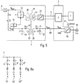
- An example of a drive by means of a clocked constant current source is shown schematically in FIG. 6b shown.
- FIG. 6b An example of a drive by means of a clocked constant current source is shown schematically in FIG. 6b shown.
- no detections of feedback variables such as, for example, the LED current, the LED voltage or the current through the switch SW1 are shown.
- the LEDs of the LED paths 8, 8 ', 8 "(which are arranged, for example, on an LED module F) are each fed by a step-down converter as a clocked constant current source via the outputs 7, 7', 7".
- the actively clocked switch of the clocked constant current source is controlled directly or indirectly (for example via a driver module) by the control unit E.
- the use of a clocked constant current source in contrast to a Linear controller flexible operation of different LED modules F.
- the clocked constant current source can adjust both the voltage and the current through the LED module F and adjust.
- the clocked constant current source is an actively clocked DC-DC converter, which receives the DC supply voltage 5 and the LED module F accordingly with the desired LED current and / or LED voltage feeds, preferably by a control by the control unit E. due to the feedback of this control unit E supplied.
- the clocked constant current source further offers the advantage that the operating mode of the submodule C can be adapted to the respective current operating mode.
- the type of timing of the clocked constant current source can be adjusted, for example, the switch SW1 can be controlled with a frequency-modulated, pulse width modulated or a combination of Frequenzmodulatorm and pulse width modulated signal.
- the current operating mode may differ, for example, for operation at high brightness of the LED track 8 and at low brightness.
- a plurality of clocked constant current sources for feeding the LED sections 8, 8 ', 8 "on the outputs 7, 7', 7" are present.
- the switches SW1, SW1 ', SW1 "of the individual clocked constant current sources can be controlled independently of one another by the control unit E.
- the individually required LED currents and LED currents for each LED paths 8, 8', 8" are made possible.
- Voltages can be supplied via the outputs 7, 7 ', 7 " also possible that in each case a separate control unit E, E ', E "for each of the clocked constant current sources with the switches SW1, SW1', SW1" is present.
- control unit E may detect various feedback quantities (such as LED voltage, LED current, or temperature) and, preferably upon detection of a fault, switch the pulsed constant current source to an error operating mode. This can be done, for example, by a change to a burst mode or a low on-time operation of the switch SW1.
- control unit E via a communication interface 6, which is designed in addition to the DC supply voltage 5, with the control unit G of the first module 1 are unidirectional or bidirectional in data communication.
- the communication interface 6 can also be used to transmit the low-voltage supply (there is then both a data communication and an energy transfer).
- the communication interface 6 can also be integrated into the DC supply voltage 5, for example, the polarity of the DC supply voltage 5 can be switched or a carrier signal to the DC supply voltage 5 are modulated.
- control unit E can also, for example in the case of error detection by means of bidirectional data communication an error message and preferably also convey information about the type of error to the control unit G of the first module 1.
- the second module here as a lamp management module, preferably housed in a common housing 12 with the actual LED module F.
- the LED module F may have its own memory 4, for example in the form of an eprom.
- the reference numeral 3 denotes schematically that the control unit E of the second module 2 can access this memory 4 of the LED module F.
- the PFC circuit is optional only.
- submodules A, B and C can also be integrated circuit-wise, so that, as long as these functions are basically present, they do not have to be reflected in a corresponding structure of the circuit topology.
- the advantage of the modular design according to Fig. 1 It is, for example, that the first module 1 and the second module 2 can be produced by different manufacturers.
- a plurality of second modules 2 in the sense of a master / slave operation can be connected to a first module 1.
- a two-stage system is created with a modular design, with several second modules 2 to a first Module 1 can be connected and also an operation of different LED modules F and / or a different operation of the same LED modules F depending on the taking place via the communication interface 6 data communication is possible.
- the modular design also allows the respective sub-modules and in particular the second module 2 to be interchangeable while retaining the remaining components.
- the communication between the first module 1 and the second module 2 via the communication interface 6 is accordingly preferably standardized.
- incoming commands or queries are supplied as shown only the first module 1.
- This can thus be referred to as external data communication, in contrast to the internal data communication via the communication interface 6 between the first module 1 and the second module 2.
- the communication via the internal communication interface 6 is thus also standardized, since it is independent of different bus protocols or control signals which can be applied to the first module 1.
- the communication via the internal communication interface 6 combined with the modular design of the system provides the advantage that the operating data for the optimal feeding of the second module 2 can be transmitted from the second module 2.
- the second module 2 (preferably starting from the control unit E) can transmit the required operating data via the internal communication interface 6 to the first module 1.
- Examples of the feedback quantities 13 from the LED track 8 are the directly or indirectly measured LED current and / or the voltage across the LED track 8.
- operating data for the LEDs of the LED track 8 can be stored, for example, at the manufacturer. These data in this memory 4 can thus be, for example, characteristic values, the permissible maximum values for current and / or voltage, temperature dependence of electrical or optical (spectra) parameters of the LEDs, etc. Also these operating data for the LEDs (for example data from the memory 4) can be transmitted to the first module 1 via the internal communication interface 6.
- a first module 1 in the sense of a master can supply a plurality of second modules 2. This means that a single first module 1 not only supplies a plurality of second modules 2 with a DC supply voltage 5, but also communicates with these bidirectionally in the sense of an internal communication interface 6.
- control unit G in the first module 1 can control the second submodule B, which is preferably clocked.
- the same control unit G or preferably also a further control unit (not shown) can also control the operation of the PFC of the first sub-module A, ie for example controlling the switch of the PFC of the sub-module A and for signals from the area of the PFC, such as the input voltage, the current through an inductance of the PFC, the current through the switch of the PFC, the output voltage of the PFC , as shown schematically by arrows in Fig. 1 is shown.
- the PFC may be, for example, a boost converter (boost converter), flyback converter (buck-boost converter, an isolated flyback converter) or SEPIC converter.
- boost converter boost converter
- flyback converter buck-boost converter
- isolated flyback converter SEPIC converter
- the output voltage (bus voltage) V bus of the PFC of the first sub-module A is in a range of several hundred volts DC. Due to the transformer 19 in the second sub-module B, therefore, this DC voltage can be lowered, for example to a voltage in the range of 20 to 60 volts, preferably 40 to 50 volts DC.
- the DC supply voltage 5 is after the output of the first module 1 in a lower level than the ruling internally in the first module 1 voltages, which for the requirements, for example, to the isolation of the DC supply voltage 5 of the second module 2 and the second Module 2 even lower claims.
- a second output voltage for example a DC low-voltage supply for the second module 2 can be generated in the first module 1 and provided to the second module 2.
- the second module 2 (or in the presence of a plurality of second modules 2 at least individual of these) can be switched off, while the first module 1 is still responsive to the communication interface 6 or possibly send 6 messages via the communication interface.
- the first module 1 can perform an emergency light detection (switching from AC to DC supply or rectified AC supply).
- the control unit G for example as a microcontroller, of the first module 1 in this idle state can only be supplied with power via the external bus 10 if the idle state of the external bus 10 (for example in the case of DALI) is not equal to 0 volts.
- an energy transmitted via the external bus 10 can be used to supply the control circuit G (in particular as start-up energy for the control circuit G or a low-voltage supply circuit).
- the actual power supply of the first module 1 can be turned off in this idle state.
- only a wake-up signal is sent via the external bus 10, which provides a starting energy as a power for short-term supply for the control circuit G or a low-voltage supply circuit.
- the first module 1 can be completely put into a resting state without energy consumption.
- the wake-up signal may also be a data transmission or a momentary connection of a voltage.
- first module 1 central module
- selectively selected ones of these several second modules 2 can be switched off become. This also leads to a saving of electrical losses.
- the emergency case it can be provided that only one or a subset of the plurality of second modules 2 supplied by the first module 1 is operated to achieve the lower basic brightness for the emergency lighting operation.
- a passive or preferably active, in particular controlled by the control unit E coolant 40 is connected, for example.
- the second module 2 (lamp management module) may also have an additional interface (not shown).
- This additional interface can be designed, for example, wired or wireless.
- data can be read out from the second module 2 via this interface, in particular for maintenance purposes, such as the replacement of a second module 2.
- the additional interface is arranged on the second module 2 spatially separated from the communication interface 6.
- the first module 1 has a second sub-module B, which has the function of an insulating converter.
- This second sub-module B is supplied starting, for example, from the PFC of the first sub-module A with a DC voltage ( bus voltage) V bus .
- This second sub-module B has a clocked insulating DC / DC converter as explained in detail below. This will now be with reference to FIG. 2 be explained.
- FIG. 2 is shown that the output voltage of the module A (eg PFCs), namely the bus voltage V bus is fed to an inverter 14, which may be formed, for example, as a half-bridge inverter with two switches S1, S2.
- the control signals for the timing of the switches S1, S2 can be generated by the control unit G of the first module 1.
- a resonant circuit 15 here designed as a series resonant circuit, namely an LLC resonant circuit, adjoins the center point 29 of the inverter 14.
- this resonant circuit 15 has a first inductor 16, a coupling capacitor 17, a transformer 19.
- the resonant circuit 15 is followed by a transformer 19 with a primary winding 20 and a secondary winding 21.
- Die Inductor 16 may be integrated into the transformer 19, as will be explained later.
- the transformer 19 is shown as an equivalent circuit diagram.
- the primary winding 20 has in reality an inductance 18 as an integrated leakage inductance and, in addition, a main inductance Lm which carries the magnetizing current.
- the transformer 19 is followed by a rectifier 22, at the output of which the lowered DC supply voltage 5 for the lamp management module 2 is provided.
- the transformer 19 thus provides the necessary galvanic decoupling (insulation with respect to the first module 1 supplied input voltage 9).
- the rectifier 22 can be designed as known per se with two or four diodes, but it can meanwhile be provided a so-called 'synchronous rectifier' (synchronous rectifier) having two MOSFETs. This synchronous rectifier performs as known per se with the two MOSFETs full bridge rectification.
- the rectifier 22 can thus be designed both as an active rectifier (with actively connected elements such as MOSFET) or as a passive rectifier (with passively connected elements such as diodes).
- a storage capacitor 23 follows the rectifier. Additional filter elements such as one or more inductors and / or additional capacitors for smoothing and stabilizing may also be present at the output the output voltage (DC supply voltage 5) may be present.
- the inductance 16 does not have to be present as a separate component. Rather, the scattering of the primary winding 20 of a real transformer can take over this function.
- the first inductance 16 is to be formed by the scattering of the primary winding 20 of the transformer 19, care is taken to ensure that there is no perfect coupling between the primary winding 20 and the secondary winding 21 of the transformer 19.
- the necessary scattering effect can be achieved in a targeted manner, which can functionally achieve the first inductance 16. While this scattering effect should not be sufficient, an inductance 16 actually present as a separate component will also be provided.
- the combination of the inverter 14 with the resonant circuit 15 and the following rectifier 22 thus forms an insulating by the transformer 19 DC / DC converter as a power transmitting converter.
- this DC / DC converter is powered by a stabilized DC voltage, the bus voltage V bus , and from this a DC supply voltage 5 is generated at the output of the DC / DC converter, which also represents a stabilized DC voltage, which compared to the bus voltage V Bus through the transformer 19 is isolated and preferably has a different potential.
- An advantage of the use of a resonant circuit in such a DC / DC converter transmitting energy lies in the exploitation of a resonant peak, in order to enable a low-loss switching of the switches S1, S2 of the inverter 14 at nominal load or high load on the secondary side. This is usually done in the vicinity of the resonance frequency of the resonant circuit or in the vicinity of a harmonic resonance of the output circuit.
- the output voltage (to the storage capacitor 23) of the transmitting converter is thus a function of the frequency of the control of the switches S1, S2 of the inverter 14, embodied here by way of example as a half-bridge inverter.
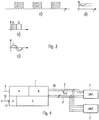
- the driving frequency of the switches S1, S2 of the inverter 14 is increased away from the resonance frequency. Meanwhile, as the driving frequency changes, the phase angle between the voltage and the AC current at the center point 29 of the inverter 14 also changes.
- the phase angle between current and voltage at midpoint 29 is very low.
- the phase angle is very big (see Figure 3c ) and may for example be up to 50 °. In this state, therefore, currents continue to flow through the inverter 14, which lead to electrical losses without any appreciable power flowing into the LED track 8.
- a combined control can be provided.
- the combined control is that for the size to be controlled 'output voltage of the energy transferring isolated converter' two control variables are used, namely in addition to the timing of the at least one switch S1, S2 of the inverter 14, the change of the bus voltage V bus of the inverter 14. Die Modification of the bus voltage V Bus can be achieved, for example, by appropriate control of the PFCs of the first submodule A.
- the bus voltage V Bus can be adjusted by appropriate control of the PFCs of the first sub-module A.
- the PFC of the first submodule A can change the operating mode either independently or through a corresponding activation, in particular by the control unit G.
- the PFC of the first sub-module A may operate in either a so-called limit operation between random and non-latching current mode (Borderline Mode) or continuous conduction mode during low-load operation, and low load or stall operation -By mode operating in discontinuous conduction mode.
- the PFC of the first submodule A changes during operation of a low load or in stand-by mode in so-called burst mode (ie a pulse-pause operating mode or pulse mode).
- burst mode ie a pulse-pause operating mode or pulse mode.
- the supply voltage bus voltage V bus
- V bus supply voltage
- the switch or switches of the PFC a longer break before the next "Burst" (pulse) is applied as a drive signal for the switches of the PFC.
- the pause between the pulse trains is much longer, that is, for example, at least twice the addition of the switch-on periods of the switches of the PFC.
- the dead time (see FIG. 3b ) between the switch-on periods of the switches S1, S2 of the inverter 14 to extend.
- the second control variable is then used to further reduce the power consumption, namely the extension of the dead time between the switch-on periods of the switches S1, S2.
- Another possibility is to change the ratio of switch-on time duration to switch-off time duration of the switches S1, S2 of the inverter 14 while the frequency remains the same (ie the switch-on ratio).
- the duty ratio is reduced as the load decreases. It is thus possible, for example, to increase the frequency increase of the power supply to a maximum permissible drive frequency of the switches S1, S2 of the inverter 14. At this maximum permissible frequency (corresponding to the maximum permissible phase angle), the second control variable is then used to further reduce the power consumption, namely the change in the switch-on duration of the switches S1, S2 (at the same frequency).
- burst mode ie a pulse-pause operating mode or also pulse mode called
- the supply voltage bus voltage V bus
- V bus the supply voltage
- the drive frequency is given a maximum permissible value
- a longer break is inserted before the next "burst" (pulse) is applied as the drive signal for the switches S1, S2.
- the pause between the pulse trains is much longer, that is, for example, at least twice the addition of the switch-on periods of the switches S1, S2.
- the next pulse train is applied, so that this rise and fall of the voltage (ripple) on the storage capacitor 23 will repeat cyclically. So there is a hysteretic regulation.
- the burst packets ie the period in which clocked for a short time
- the bursts may also be generated at a variable repetition rate and / or duration of the packets.
- the submodule C is designed as a clocked constant current source, then the ripple occurring in the burst operating mode can be the DC supply voltage 5 are compensated by a corresponding control of the clocked constant current source. This can be done for example by means of a control loop for a compensation of the LED current or an operation of the clocked constant current source as a function of the amplitude of the DC supply voltage 5.
- the adaptive adjustment of the operating mode (control variable) of the DC-DC converter is dependent on the load on the secondary side, ie the load supplied by the voltage on the storage capacitor 23.
- a load reproducing the signal to the drive circuit (IC in the control circuit G in Fig. 1 ), or an externally supplied dimming signal can be used.
- the power consumption of the load can be measured on the secondary side (with respect to the transformer 19), but also on the primary side of the transformer 19.
- the voltage drop across a measuring resistor 24 in series with the switches S1, S2 or at least in series with one of the switches S1, S2 of the inverter 14 may be used.
- the actual power consumption then essentially constitutes a product of the supply voltage ( bus voltage V bus ) (measured or at least kept constant by the PFC) with this current measured by the inverter 14 via the voltage drop across the measuring resistor 24.
- a primary-side detection was given for a signal representing the power consumption of the load.
- secondary-side feedback signals such as the current be used by the and / or the voltage across the LED track 8, etc. as feedback signal, which feedback signal reflects the power consumption of the load.
- a preferred sequence of adaptive combined control is to perform the reduction for the load by continuously increasing the drive frequency of the switches S1, S2 of the inverter 14 until a fixed maximum frequency is reached. When this maximum frequency is reached, but the power supplied to the load is to be further reduced, the drive circuit will then adaptively select one of the other modes listed above. If, for example, when the permissible maximum frequency is reached, the bus voltage V Bus is lowered, then the permissible maximum frequency of the control of the switches S1, S2 can be maintained, or even if this can be overcompensated by lowering the bus voltage Vbus or the other selected control variable, the drive frequency even be lowered back to a lower setpoint range.
- the sub-module B can also be formed by an inverter with a switch, for example as a Class-E converter or quasi-resonant flyback converter, wherein in each case a rectification and smoothing takes place at the output.
- a second module 2 with a further converter stage can be connected to the storage capacitor 23, wherein the second module 2 (lamp management module) can have a control unit E, eg as an integrated circuit.
- the further submodule C can be embodied both as a clocked constant current source (that is to say for example as a step-down converter, ie Buck converter) or as a linear regulator (realized with transistors or integrated circuits). But it can also be directly connected to the output of the second sub-module B LEDs.
- External dimming commands can, as in Fig. 1 represented, the control unit G of the first module 1, but also the control unit E of the second module 2 are supplied.
- the control unit E of the second module 2 can transmit the dimming information to the control unit G of the first module 1, so that no measurement signal must be present for the power consumption, but rather from one the control unit G for the DC-DC converter in the second module B present dimming information can be used.
- the adaptive adjustment of the second submodule B can, however, also take place on the basis of a dimming command supplied externally or else due to feedback by the second module 2.
- the control of the switches S1, S2 of the inverter 14 can be done via the control unit G via a driver stage.
- a driver stage Preferably, at least the driver stage for the high-potential switch of the inverter is designed for driving at a high voltage potential.
- this driver stage is a level offset stage, a driver stage with a transformer or a driver stage with an air coil. This driver stage can also be integrated in the control unit G.
- the control unit G may further comprise means for avoiding errors in the operation of the inverter. For example, over-current shut-offs or current limits for the current may be present through at least one switch. It is also possible to set the dead time for the drive of the inverter (ie the time between the opening of the one switch (eg S1) and the closing of the second switch (S2)). Preferably, this dead time is adaptively adjustable, for example, depending on the midpoint voltage at the inverter 14 or the current or the voltage across a switch of the inverter 14th
- the control unit G can also monitor the bus voltage V Bus , in particular also the ripple of the bus voltage V Bus (ie the fluctuations within a certain time). Depending on the evaluation of the ripple of the bus voltage V Bus , the control unit G can influence the control of the inverter 14. In particular, it can adapt the frequency of the inverter 14 to the evaluation of the ripple of the bus voltage V Bus in order to reduce the ripple at the output of the inverter 14. Preferably, the frequency of the inverter is increased with increasing bus voltage bus, and lowered with decreasing bus voltage V bus . In this way it can be achieved that this ripple on the bus voltage V bus is less continued to the output of the inverter 14.
- the communication interface 6 (internal bus) between the first module 1 and one or more second modules 2, 2 'will be explained as lamp management modules.
- the first module 1 Due to the fact that via the internal bus several second modules 2, 2 'not only with power (transmission path 5), but also unidirectionally or bidirectionally by means of data communication (via the communication interface 6), the first module 1 as a central unit or master.
- the second modules 2, 2 ' may be referred to as slaves.
- a preferably standardized communication is provided, which is provided in addition to the DC supply voltage 5.
- standardized is meant that the protocol of the communication interface 6 is independent of the external communication protocol via the data interface 11 of the first module 1.
- the communication via the communication interface 6 is bi-directional and can be done, for example, according to a SPI protocol (Serial Peripheral Interface).
- SPI protocol Serial Peripheral Interface
- the data communication via the communication interface 6 is preferably electrically isolated, for example using optocouplers or transformers.
- the transformer can be clocked at high frequency and thus transmit data via packets of high-frequency clocks.
- the potential-separated design of the communication interface 6 also increases the robustness of the illumination system, for example, the separation and replacement of a second module 2 is facilitated.
- a fundamental function of the communication interface 6 may be the transmission of dimming commands from the first module 1 to the second modules 2, which have been received via the external bus 10, for example.
- new control information or commands for the second modules 2 can also be derived from the dimming commands received via the external bus 10.
- One application for bidirectional data communication via the internal bus is that data stored in one of the second modules 2, 2 'is sent to the computer via the internal bus (communication interface 6) Control unit G of the first module 1 can be transmitted.
- This is advantageous in that the data storage in the second modules 2, 2 'is closer to the LED track 8, so that there is a higher heating, which leads to a possibly irreproducible loss of data storage in the field of lamp management modules ( second modules 2, 2 ') can follow.
- these data can then be the first module 1 in the sense of a backup again stored.
- Examples of this data transmitted via the communication interface 6 are operating data for the LED route 8, such as temperatures, operating times, electrical parameters, etc.
- the standardized approach for the internal bus also has the advantage that lamp management modules (second modules 2, 2 ') can be exchanged in a simple manner.
- the supply in a lamp management module to be exchanged (second modules 2, 2 ') stored data can already be described above after transmission via the communication interface 6 in the first module 1 are stored. If then the lamp management module is replaced, the stored in the first module 1 operating data can be transferred back to the newly installed lamp management module so that it is then configured identically to the replaced lamp management module.
- Such operating data are color coordinates, color coordinates or other parameters influencing the spectrum of the LED route 8.
- the first module 1 receives dimming commands via the external bus 10 and the data interface 11 or the interface circuit D, which indicate a load change of the LED route 8, such information or a signal representing the operating state change can be transmitted via the bus or the communication interface 6 are transmitted to the second modules 2, 2 ', so that the control unit E provided in the second modules 2, 2' can also adapt control parameters, for example for the constant current source (further submodule C) in accordance with the expected load change.
- This in FIG. 4 shown master / slave system also has advantages in terms of reducing electrical losses, since a kind of standby mode can be provided in which one, several, or even all of the second module 2, 2 'connected to a first module 1 are turned off, while at least the control unit G of the first module 1 can continue to monitor the externally connected bus 10 via the data interface 11 or the interface circuit D.
- FIG. 4 illustrated master / slave system preferably only via the connected to the data interface 11 and the interface circuit D of the first module 1 bus 10 responsive.
- an addressed communication can take place towards the second modules 2, 2 '.
- a broadcast mode may also be provided, i. an undressed data transmission from the first module 1 to all connected second modules 2, 2 '.
- a command transmitted by the first module 1 via the internal bus (communication interface 6) is received and evaluated by all second modules 2, 2 '.
- a corresponding control command is transmitted via the communication interface 6 and the second modules 2, 2 'are adapted according to their operation. For example, to achieve a lower basic brightness and thus a lower energy consumption for emergency lighting operation, only one or a subset of the plurality of second modules 2 supplied by the first module 1 can be operated.
- the communication interface 6 can also be used to transmit the low-voltage supply (then there is both a data communication and an energy transfer, for example via the secondary-side DC low-voltage supply V CCs ).
- a so-called active low data transmission can be used, wherein at rest, a level of a few volts, for example 12V, is applied.
- a coupling for example via transformers could thus also in a galvanic separation of Communication interface 6 still be transmitted energy.
- a low-voltage supply for example, by a second module 2 (lamp management module) active coolant 40, such as a fan, a pump, a Peltier element, etc. can be supplied.
- active coolant 40 is thus not supplied directly from the first module 1, but preferably individually via each connected lamp management module 2 with electrical power.
- FIG. 5 is again shown how the bus voltage V bus , for example, generated by the PFC module of the first module 1, an inverter is supplied.
- the inverter has only one switch S1 in contrast to the inverter 14 as a half-bridge inverter of Fig. 2 on.
- the primary winding 20 of the transformer 19 is shown following the inverter with the switch S1.
- a rectifier 22 is supplied, in which the output voltage of the rectifier 22 directly or indirectly the LED track 8 is supplied.
- the primary and secondary windings 20, 21 represent the already explained above path to the electrical power supply (DC supply voltage 5) of the LED track of the LED module F.
- inverter In the inverter according to Fig. 5 It can be a converter with one or more switches, such as a half-bridge inverter (see example Fig.2 ) or isolated flyback converters. Preferably, this works resonantly or quasi-resonantly.
- a further low-voltage transmission path This has a further secondary winding 30, which is therefore also magnetically coupled to the primary winding 20.
- a rectifier circuit having a diode 31 and a capacitor 32
- a secondary-side DC low-voltage power supply V CCS is generated by appropriately selecting the winding ratios of the windings 20, 30. Also shown in the figure, this secondary-side DC low-voltage power supply V CCS is also supplied to the second module 2.
- yet another (and thus third) secondary winding 33 is magnetically coupled to the primary winding 20 of the transformer 19.
- This secondary winding 33 feeds a rectifier with a diode 42 and a capacitor 43, serves to generate a primary-side low-voltage power supply V CCP .
- this low-voltage power supply V CCP is used in the first module 1 (ie on the network side, ie before electrical isolation), for example, as a low-voltage power supply for the internal integrated control unit G of the first module. 1
- the power transfer across the DC power supply 5 supply to the LED module F may be 48 volts DC
- the voltage levels of the low voltage power supplies V CCS and V CCP are significantly lower, for example in the range of 2 to 12 volts DC.
- the lighting system can also be operated such that the second sub-module B deactivates the supply of the DC supply voltage 5 and only the low-voltage supply (for example, the secondary-side DC low-voltage supply V CCs ) is maintained. This can be done, for example, in an error mode or idle mode. In this way, for example, existing sensors such as the sensor 41 can continue to be evaluated and, for example, the communication interface 6 can remain activated. Preferably, furthermore, the control unit E continues to operate at least in a reduced operating mode (for example, with reduced functionality).
- a reduced operating mode for example, with reduced functionality
- the sensor 41 which is functionally associated with the second module 2, may be a brightness sensor, for example a photodiode with optional evaluation logic, or a color sensor.
- the sensor 41 which is functionally associated with the second module 2, can of course also be a temperature sensor whose output signal can be used, for example, to determine the temperature of the LED junction of the LEDs of the LED module F.
- this sensor 41 can also be used as a temperature sensor for regulating the operation of the active cooling, for example of the coolant 40 (preferably as a fan).
- a temperature determination of the temperature of the LED junction by evaluating the characteristic and measuring electrical parameters of the LED route of the LED module F done.
- FIG. 2 and FIG. 5 can recognize an inverter with a switch S1 or more switches S1, S2 are present.
- Inverter 14 shown as a half-bridge inverter are called the flyback converter, a SEPIC or a forward converter. In any case, there is an isolated converter.
- a starting resistor R1 which supplies the control unit G with energy until the primary-side low-voltage supply V CCP is generated as expected, since the generation of the primary-side and also the secondary-side low-voltage supplies V CCP and V CCS requires a clocking of the second sub-module B (DC / DC converter). If the actual low-voltage power supply then started from the isolated converter (second sub-module B), the ohmic starting resistor R1 can be switched off again with the switch S3, so as to avoid electrical losses via the starting resistor R1 in the regular operation of the circuit.
- the low-voltage power supplies V CCS , V CCP are obtained by means of a full-bridge rectifier. But it can also be used only a single diode for rectification.
- the low-voltage power supply V CCS can be supplied to a control unit E in the second module 2 and / or can be looped further for the supply of an active coolant 40 assigned to the second module 2.
- the secondary DC low voltage power supply V CCS for the second module 2 can be used for voltage stabilization as in FIG. 5 shown again a coolant control 50, for example, a DC / DC converter or a linear regulator are supplied, in which case the stabilized output voltage of this DC / DC converter or linear regulator 50 feeds the control unit E of the second module 2.
- the coolant control device 50 may depend on a dimming command (dimming information) supplied via the communication interface 6, on a specification by the control unit E or also on the temperature determined directly (via a temperature sensor) or indirectly (for example a temperature determination of the temperature of the LED junction) on the LED module F control the control of the active coolant 40 or regulate.
- active coolant 40 can be supplied by such a low-voltage supply via a coolant control 50, which is arranged in each case on the second module 2.
- active coolant 40 is thus not supplied directly from the first module 1, but preferably individually via each connected lamp management module 2 with electrical power.
- This offers the advantage that in an operation of several second modules 2, 2 '... via a first module 1 for each second module an independent control of active coolant 40 is possible. This can be particularly advantageous if the brightness of the individual LED modules F is different or due to the spatial arrangement of the individual LED modules F a different degrees of heating of the LED modules F takes place.
- the low-voltage supply can also serve as a communication interface 6, ie data can also be transmitted in addition to the transmitted energy.
- the LED module F may be provided in a memory 4 associated with it, for example with an EPROM, FLASH or OTP.
- the control unit E for example, an integrated circuit or a microcontroller of the second module 2 access the memory 4 of the LED module F, thus, for example, selectively read out the memory contents.
- the data read out from this memory 4 can then also be sent, for example, from the control unit E of the second module 2 to the first module 1 via the communication interface 6 (internal bus).
- the data in the memory 4 may be, for example, the runtime, manufacturing data, error logging, maximum value, minimum values (eg for current and voltage) and / or the temperature.
- control unit E of the second module 2 read this data and store it in a memory associated with it in the sense of a backup.
- the control unit E of the second module 2 can refresh the memory 4 of the LED module F periodically or depending on the operating state or event.
- the LED module F itself has no memory.
- the corresponding data, for example the permissible forward current for the LEDs of the LED track 8 can in this case be written in the memory 51 assigned to the control unit E of the second module 2. This can be done during the production of the second module 2, for example.
- the LED module F is provided with an identification tag which represents, for example, the operating data or at least represents an identification for the LED module F.
- the identification tag is then read out by the control unit E of the second module 2 and stored, for example, in a memory assigned to the control unit E of the second module 2. This thus only once read data content of the identification tag can then be used for the further operation of the LED module F.
- the identification tag can only be a pure identification.
- the lamp management module (second module 2) would determine the identification data and then determine operating data independent of the LED module F, for example also a database content accessible via the external bus 10.
- the approach has the advantage that thus the cost of the additional memory 4, for example, an Eprom of the LED module F can be saved.
- the possibility of reading out the memory 4 of the LED module F by the control unit E gives the advantage that a very different LED modules F can be combined with a lamp management module (second module 2), wherein the required operating data can be read out of the LED module F and the lamp management module (second module 2) thus flexibly the connected LED module F can adjust.
- the LED module F as shown schematically in FIG. 6a . 6b already shown, two, three or even more independently controllable channels 53, 53 ', 53 "in.
- Each channel 53, 53', 53" may have an LED track 8, 8 ', 8 "with one or more LEDs.
- the aim is that the different LED channels 53, 53 ', 53 "of the LED module F in the color space span a space within which the desired controllable color coordinates lie.
- an embodiment of the two or more LED channels 53, 53 ', 53 "of the LED module F is preferred such that the encompassed space comprises at least large areas of the Planck's white light curve.
- each color locus can be controlled within the triangle formed thereby.
- the example above spans a triangle in color space that covers at least large areas of Planck's white light curve.
- the total light output should now remain constant even when departing from different color loci, in particular on the Planck's white light curve.
- the drive intensities can then be calibrated for all other color loci to be approached, i. the intensities are scaled down 'artificially' for each color location deviating from the minimum light output, so that in the end, in the spanned color space, light is generated constantly with the minimum achievable light output.
- the calibration factor can be calculated based on the known efficiencies of the LEDs used.
- the total light output when departing different color locations in particular in the manner of a scan of Planck's white light curve with simultaneous measurement
- Such a measurement thus determines, on the one hand, the minimum total light output within the color loci to be removed and the dependence of the total light output on the color locus.
- the calibration factor for reducing the intensities of the individual LED paths in terms of PWM dimming can be performed.
- the calibration is generated by a reduction in the duty cycle of a PWM drive.
- this can also be done by adjusting the amplitude (in the sense of amplitude dimming).
- the calibration can be done on an adjustment of the amplitude.
- the said intensity scan can be carried out repeatedly, since the different LEDs have different aging phenomena with respect to their efficiency (intensity per current) must be compensated and can lead to different efficiencies.
- a dye-converted LED will have a higher degree of aging than monochromatic LEDs.
- said intensity scan can also be used for monitoring the aging when the operating data of the LED are known (for example stored in the memory 4 of the LED module F).
- aging parameters can already be determined by the manufacturer and, for example, stored in the memory 4, which is assigned to the LED module F.
Landscapes
- Circuit Arrangement For Electric Light Sources In General (AREA)
Claims (12)
- Système d'éclairage à LED comprenant :- un premier module (1) avec un deuxième sous-module (B), de préférence un convertisseur DC/DC qui est conçu pour être alimentée avec une tension d'entrée (9), de préférence une tension d'alimentation AC et- un deuxième module (2), de préférence un module de gestion de lampe, qui est conçu pour alimenter un sous-module supplémentaire (C) alimenté à partir du deuxième sous-module (B), de préférence une source de courant constant, qui est conçu pour alimenter au moins un module à LED (F),le premier module (1) étant conçu pour mettre à disposition, parallèlement à l'alimentation du sous-module supplémentaire (C), au moins une alimentation à basse tension (Vccs) pour le deuxième module (2),
caractérisé en ce que
l'alimentation à basse tension (Vccs) est en outre conçue pour servir également d'interface de communication (6) entre le premier module (1) et le deuxième module (2). - Système d'éclairage à LED selon la revendication 1, le système d'éclairage à LED étant conçu de façon à ce que l'alimentation à basse tension (Vccs) est introduite dans le module supplémentaire (2) d'une unité de commande (E) et/ou rebouclée pour l'alimentation d'un fluide de refroidissement actif (40) correspondant au deuxième module (2).
- Système d'éclairage à LED selon l'une des revendications précédentes, le système d'éclairage à LED étant conçu de façon à ce que l'alimentation à basse tension (Vccs) pour l'unité de commande (E) soit stabilisée par une commande de fluide de refroidissement (50), de préférence un convertisseur DC/DC, dans le deuxième module (2).
- Système d'éclairage à LED selon l'une des revendications précédentes, le convertisseur DC/DC comprenant, dans le premier module (1), un transformateur (19) qui est conçu de façon à ce que la tension d'alimentation (5) pour le sous-module supplémentaire (C) et l'alimentation à basse tension (Vccs) soient extraites à partir de celui-ci.
- Système d'éclairage à LED selon la revendication 4, le transformateur (19) est conçu de façon à ce qu'une alimentation à basse tension (VCCP) pour le premier module (1), plus particulièrement une unité de commande (G) de celui-ci, soit également extraite à partir de celui-ci.
- Système d'éclairage à LED selon la revendication 5, le système d'éclairage à LED étant conçu de façon à ce que les alimentations à basse tension (VCCP, Vccs) pour le premier module (1) ou le deuxième module (2) soient extraites par l'intermédiaire de spires secondaires isolées galvaniquement (33, 30) du transformateur (19).
- Procédé de génération d'une alimentation à basse tension dans un système d'éclairage à LED, moyennant quoi :- un premier module (1) du système d'éclairage à LED est alimenté avec un deuxième sous-module (B), de préférence un convertisseur DC/DC, avec une tension d'entrée (9), de préférence une tension d'alimentation AC et- un deuxième module (2) du système d'éclairage à LED alimente un sous-module supplémentaire (C), alimenté à partir du deuxième sous-module (B), qui alimente au moins un module à LED (F),le premier module (1) transmet parallèlement à l'alimentation du sous-module supplémentaire (C) au moins une alimentation à basse tension (Vccs) au deuxième module (2),
caractérisé en ce que
l'alimentation à basse tension (Vccs) sert également d'interface de communication (6) entre le premier module (1) et le deuxième module (2). - Procédé selon la revendication 7,
l'alimentation à basse tension (Vccs) étant introduite dans le deuxième module (2) d'une unité de commande (E) et/ou est rebouclée pour l'alimentation d'un fluide de refroidissement actif (40) correspondant au deuxième module (2). - Procédé selon l'une des revendications précédentes 7 ou 8,
l'alimentation à basse tension (VCCS) pour l'unité de commande (E) dans le deuxième module (2) est stabilisée par une commande de fluide de refroidissement (50), de préférence un convertisseur DC/DC. - Procédé selon l'une des revendications précédentes 7 à 9,
la tension d'alimentation DC (5) pour le sous-module supplémentaire (C) et l'alimentation à basse tension (Vccs) étant extraites à partir d'un transformateur (19) dans le deuxième sous-module (B) du premier module (1). - Procédé selon l'une des revendications 7 à 10,
une alimentation à basse tension (VCCP) pour le premier module (1), plus particulièrement une unité de commande (G) de celui-ci, une alimentation à basse tension (VCCP) étant également extraite à partir du transformateur (19). - Procédé selon la revendication 11,
les alimentations à basse tension (VCCP, Vccs) pour le premier module (1) ou le deuxième module (2) étant extraites par des spires secondaires isolées galvaniquement (33, 30) du transformateur (19).
Applications Claiming Priority (3)
| Application Number | Priority Date | Filing Date | Title |
|---|---|---|---|
| DE102010003057 | 2010-03-19 | ||
| DE102010031247A DE102010031247A1 (de) | 2010-03-19 | 2010-07-12 | Niedervolt-Spannungsversorgung für ein LED-Beleuchtungssystem |
| PCT/EP2011/054235 WO2011113958A1 (fr) | 2010-03-19 | 2011-03-21 | Alimentation basse tension pour un système d'éclairage à del |
Publications (2)
| Publication Number | Publication Date |
|---|---|
| EP2548410A1 EP2548410A1 (fr) | 2013-01-23 |
| EP2548410B1 true EP2548410B1 (fr) | 2017-06-14 |
Family
ID=44585470
Family Applications (1)
| Application Number | Title | Priority Date | Filing Date |
|---|---|---|---|
| EP11709936.6A Active EP2548410B1 (fr) | 2010-03-19 | 2011-03-21 | Alimentation basse tension pour un système d'éclairage à del |
Country Status (3)
| Country | Link |
|---|---|
| EP (1) | EP2548410B1 (fr) |
| DE (2) | DE102010031247A1 (fr) |
| WO (1) | WO2011113958A1 (fr) |
Families Citing this family (14)
| Publication number | Priority date | Publication date | Assignee | Title |
|---|---|---|---|---|
| US8890414B2 (en) | 2011-04-01 | 2014-11-18 | Cree, Inc. | Lighting module |
| DE102012014308A1 (de) * | 2012-04-13 | 2013-10-17 | Tridonic Gmbh & Co. Kg | Betriebsgerät für ein Leuchtmittel und Verfahren zum Betreiben eines Betriebsgeräts |
| DE102012103229B4 (de) * | 2012-04-13 | 2019-04-18 | Hadler Gmbh | Beleuchtungsvorrichtung mit einem Betriebs- und Steuergerät und wenigstens einem damit elektronisch verbundenen LED Leuchtmittel mit wenigstens einer LED |
| DE102012007746A1 (de) * | 2012-04-18 | 2013-10-24 | Minebea Co., Ltd. | Ansteuerschaltung für LED-Hintergrundbeleuchtung |
| AT13829U1 (de) * | 2012-08-31 | 2014-09-15 | Tridonic Gmbh & Co Kg | Betriebsgerät zur Ansteuerung einer LED-Strecke mit sekundärseitiger Steuereinheit |
| DE102012109274A1 (de) * | 2012-09-28 | 2014-04-03 | Osram Opto Semiconductors Gmbh | Optoelektronisches Bauelement, Verfahren zum Herstellen eines optoelektronischen Bauelementes, Verfahren zum Betreiben eines optoelektronischen Bauelementes |
| AT14080U1 (de) * | 2013-08-12 | 2015-04-15 | Tridonic Gmbh & Co Kg | Ansteuerschaltung für ein Betriebsgerät für Leuchtmittel |
| US9241380B2 (en) | 2014-03-04 | 2016-01-19 | Osram Sylvania Inc. | Hybrid dimming control techniques for lighting drivers |
| DE102014104447B4 (de) * | 2014-03-28 | 2025-12-04 | Inventronics Gmbh | Elektronisches Vorschaltgerät für LED-Leuchtmittel |
| DE102015207308B4 (de) * | 2015-04-22 | 2025-11-13 | Tridonic Gmbh & Co Kg | Schnittstellenschaltung mit Niedervoltversorgung für eine Steuereinheit |
| DE102015208006A1 (de) * | 2015-04-30 | 2016-11-03 | Zumtobel Lighting Gmbh | Leuchte und Verfahren zum Betreiben der Leuchte |
| DE102018110334A1 (de) * | 2018-04-30 | 2019-10-31 | Tridonic Gmbh & Co Kg | Betriebsgerät für Leuchtmittel mit einem Resonanzwandler und einer Helligkeitssteuerung |
| DE102018133151B4 (de) * | 2018-12-20 | 2021-01-21 | Vossloh-Schwabe Deutschland Gmbh | Betriebsschaltung mit zwei Wandlerschaltungen und zwei separaten Steuereinrichtungen |
| DE102019201589A1 (de) * | 2019-02-07 | 2020-08-13 | Osram Gmbh | Schaltungsanordnung zum versorgen eines kommunikationsbusses mit leistung sowie entsprechendes betriebsgerät |
Family Cites Families (12)
| Publication number | Priority date | Publication date | Assignee | Title |
|---|---|---|---|---|
| FI104034B (fi) * | 1998-03-30 | 1999-10-29 | Teknoware Oy | Menetelmä ja laite tehon syöttämiseksi valodiodeille |
| WO2001058218A1 (fr) * | 2000-02-03 | 2001-08-09 | Koninklijke Philips Electronics N.V. | Ensemble d'alimentation destine a un module d'eclairage de del |
| DE102004002018A1 (de) * | 2004-01-14 | 2005-08-04 | Tridonicatco Gmbh & Co. Kg | DC-versorgte Betriebsmittel-Module für Leuchtmittel |
| US7646029B2 (en) * | 2004-07-08 | 2010-01-12 | Philips Solid-State Lighting Solutions, Inc. | LED package methods and systems |
| US7923943B2 (en) * | 2006-01-10 | 2011-04-12 | Microsemi Corp.—Analog Mixed Signal Group Ltd. | Secondary side post regulation for LED backlighting |
| US20080018261A1 (en) * | 2006-05-01 | 2008-01-24 | Kastner Mark A | LED power supply with options for dimming |
| WO2007147242A1 (fr) * | 2006-06-19 | 2007-12-27 | Theoreme Innovation Inc. | Lampe à del |
| DE202007008155U1 (de) * | 2007-03-28 | 2007-12-13 | Glp German Light Products Gmbh | Leuchte zum Betreiben einer Leuchte |
| JP4970232B2 (ja) * | 2007-12-12 | 2012-07-04 | 株式会社小糸製作所 | 車両用灯具 |
| JP5435912B2 (ja) * | 2008-08-29 | 2014-03-05 | シャープ株式会社 | 電源装置及び照明装置 |
| DE102008044956B4 (de) * | 2008-08-29 | 2012-03-29 | Osram Ag | Beleuchtungsvorrichtung zum Einbau in eine Platte |
| DE202008012421U1 (de) * | 2008-09-18 | 2010-02-11 | Zumtobel Lighting Gmbh & Co. Kg | LED-Betriebsgerät |
-
2010
- 2010-07-12 DE DE102010031247A patent/DE102010031247A1/de not_active Withdrawn
-
2011
- 2011-03-21 DE DE112011100967T patent/DE112011100967A5/de not_active Withdrawn
- 2011-03-21 EP EP11709936.6A patent/EP2548410B1/fr active Active
- 2011-03-21 WO PCT/EP2011/054235 patent/WO2011113958A1/fr not_active Ceased
Non-Patent Citations (1)
| Title |
|---|
| None * |
Also Published As
| Publication number | Publication date |
|---|---|
| EP2548410A1 (fr) | 2013-01-23 |
| DE102010031247A1 (de) | 2011-09-22 |
| WO2011113958A1 (fr) | 2011-09-22 |
| DE112011100967A5 (de) | 2013-01-24 |
Similar Documents
| Publication | Publication Date | Title |
|---|---|---|
| EP2556726B1 (fr) | Système d'éclairage à del modulaire, à fonction d'éclairage d'urgence | |
| EP2548408B1 (fr) | Système d'éclairage à led avec un mémoire pour stocker des donnés opérationelles | |
| EP2548411B1 (fr) | Système d'éclairage à del modulaire | |
| EP2556725B1 (fr) | Système d'éclairage del modulaire à fonction de lumière de secours | |
| EP2548410B1 (fr) | Alimentation basse tension pour un système d'éclairage à del | |
| EP2548295B1 (fr) | Circuit de commande de del comprenant un convertisseur cc/cc isolant | |
| WO2011113948A1 (fr) | Système d'éclairage à del modulaire équipé d'un bus interne | |
| DE102012007478B4 (de) | Wandler für ein Leuchtmittel, LED-Konverter und Verfahren zum Betreiben eines Wandlers | |
| EP2548409B1 (fr) | Commande d'une chaîne de diodes électroluminescentes par une surce de courant constante commutée | |
| DE112009002526B4 (de) | Leuchtmittel-Betriebsgerät mit Potentialtrennung, LED-Lampe, Leuchte und integrierte Steuereinheit | |
| EP2795998B1 (fr) | Circuit de commande de led avec convertisseur resonant | |
| EP2548412B1 (fr) | Système d'éclairage à del | |
| EP3105995A1 (fr) | Circuit d'attaque de led | |
| DE112014002525T5 (de) | Steuerschaltung und Verfahren zum Erzeugen einer Spannung für eine Licht emittierende Dioden-Beleuchtungsvorrichtung | |
| EP2939501B1 (fr) | Fonctionnement de dispositifs lumineux au moyen d'un convertisseur résonant | |
| EP2783551B1 (fr) | Détection de connexion d'unités del | |
| DE102014104447A1 (de) | Elektronisches Vorschaltgerät für LED-Leuchtmittel | |
| DE102013222892B4 (de) | LED-Konverter und Verfahren zum Steuern einer Wandlerschaltung eines LED-Konverters |
Legal Events
| Date | Code | Title | Description |
|---|---|---|---|
| PUAI | Public reference made under article 153(3) epc to a published international application that has entered the european phase |
Free format text: ORIGINAL CODE: 0009012 |
|
| 17P | Request for examination filed |
Effective date: 20120910 |
|
| AK | Designated contracting states |
Kind code of ref document: A1 Designated state(s): AL AT BE BG CH CY CZ DE DK EE ES FI FR GB GR HR HU IE IS IT LI LT LU LV MC MK MT NL NO PL PT RO RS SE SI SK SM TR |
|
| DAX | Request for extension of the european patent (deleted) | ||
| STAA | Information on the status of an ep patent application or granted ep patent |
Free format text: STATUS: EXAMINATION IS IN PROGRESS |
|
| 17Q | First examination report despatched |
Effective date: 20161213 |
|
| GRAP | Despatch of communication of intention to grant a patent |
Free format text: ORIGINAL CODE: EPIDOSNIGR1 |
|
| STAA | Information on the status of an ep patent application or granted ep patent |
Free format text: STATUS: GRANT OF PATENT IS INTENDED |
|
| INTG | Intention to grant announced |
Effective date: 20170327 |
|
| GRAS | Grant fee paid |
Free format text: ORIGINAL CODE: EPIDOSNIGR3 |
|
| GRAA | (expected) grant |
Free format text: ORIGINAL CODE: 0009210 |
|
| STAA | Information on the status of an ep patent application or granted ep patent |
Free format text: STATUS: THE PATENT HAS BEEN GRANTED |
|
| AK | Designated contracting states |
Kind code of ref document: B1 Designated state(s): AL AT BE BG CH CY CZ DE DK EE ES FI FR GB GR HR HU IE IS IT LI LT LU LV MC MK MT NL NO PL PT RO RS SE SI SK SM TR |
|
| REG | Reference to a national code |
Ref country code: GB Ref legal event code: FG4D Free format text: NOT ENGLISH |
|
| REG | Reference to a national code |
Ref country code: CH Ref legal event code: EP Ref country code: AT Ref legal event code: REF Ref document number: 902068 Country of ref document: AT Kind code of ref document: T Effective date: 20170615 |
|
| REG | Reference to a national code |
Ref country code: IE Ref legal event code: FG4D Free format text: LANGUAGE OF EP DOCUMENT: GERMAN |
|
| REG | Reference to a national code |
Ref country code: DE Ref legal event code: R096 Ref document number: 502011012434 Country of ref document: DE |
|
| REG | Reference to a national code |
Ref country code: NL Ref legal event code: MP Effective date: 20170614 |
|
| REG | Reference to a national code |
Ref country code: LT Ref legal event code: MG4D |
|
| PG25 | Lapsed in a contracting state [announced via postgrant information from national office to epo] |
Ref country code: HR Free format text: LAPSE BECAUSE OF FAILURE TO SUBMIT A TRANSLATION OF THE DESCRIPTION OR TO PAY THE FEE WITHIN THE PRESCRIBED TIME-LIMIT Effective date: 20170614 Ref country code: ES Free format text: LAPSE BECAUSE OF FAILURE TO SUBMIT A TRANSLATION OF THE DESCRIPTION OR TO PAY THE FEE WITHIN THE PRESCRIBED TIME-LIMIT Effective date: 20170614 Ref country code: LT Free format text: LAPSE BECAUSE OF FAILURE TO SUBMIT A TRANSLATION OF THE DESCRIPTION OR TO PAY THE FEE WITHIN THE PRESCRIBED TIME-LIMIT Effective date: 20170614 Ref country code: GR Free format text: LAPSE BECAUSE OF FAILURE TO SUBMIT A TRANSLATION OF THE DESCRIPTION OR TO PAY THE FEE WITHIN THE PRESCRIBED TIME-LIMIT Effective date: 20170915 Ref country code: FI Free format text: LAPSE BECAUSE OF FAILURE TO SUBMIT A TRANSLATION OF THE DESCRIPTION OR TO PAY THE FEE WITHIN THE PRESCRIBED TIME-LIMIT Effective date: 20170614 Ref country code: NO Free format text: LAPSE BECAUSE OF FAILURE TO SUBMIT A TRANSLATION OF THE DESCRIPTION OR TO PAY THE FEE WITHIN THE PRESCRIBED TIME-LIMIT Effective date: 20170914 |
|
| PG25 | Lapsed in a contracting state [announced via postgrant information from national office to epo] |
Ref country code: NL Free format text: LAPSE BECAUSE OF FAILURE TO SUBMIT A TRANSLATION OF THE DESCRIPTION OR TO PAY THE FEE WITHIN THE PRESCRIBED TIME-LIMIT Effective date: 20170614 Ref country code: SE Free format text: LAPSE BECAUSE OF FAILURE TO SUBMIT A TRANSLATION OF THE DESCRIPTION OR TO PAY THE FEE WITHIN THE PRESCRIBED TIME-LIMIT Effective date: 20170614 Ref country code: LV Free format text: LAPSE BECAUSE OF FAILURE TO SUBMIT A TRANSLATION OF THE DESCRIPTION OR TO PAY THE FEE WITHIN THE PRESCRIBED TIME-LIMIT Effective date: 20170614 Ref country code: RS Free format text: LAPSE BECAUSE OF FAILURE TO SUBMIT A TRANSLATION OF THE DESCRIPTION OR TO PAY THE FEE WITHIN THE PRESCRIBED TIME-LIMIT Effective date: 20170614 Ref country code: BG Free format text: LAPSE BECAUSE OF FAILURE TO SUBMIT A TRANSLATION OF THE DESCRIPTION OR TO PAY THE FEE WITHIN THE PRESCRIBED TIME-LIMIT Effective date: 20170914 |
|
| PG25 | Lapsed in a contracting state [announced via postgrant information from national office to epo] |
Ref country code: RO Free format text: LAPSE BECAUSE OF FAILURE TO SUBMIT A TRANSLATION OF THE DESCRIPTION OR TO PAY THE FEE WITHIN THE PRESCRIBED TIME-LIMIT Effective date: 20170614 Ref country code: SK Free format text: LAPSE BECAUSE OF FAILURE TO SUBMIT A TRANSLATION OF THE DESCRIPTION OR TO PAY THE FEE WITHIN THE PRESCRIBED TIME-LIMIT Effective date: 20170614 Ref country code: CZ Free format text: LAPSE BECAUSE OF FAILURE TO SUBMIT A TRANSLATION OF THE DESCRIPTION OR TO PAY THE FEE WITHIN THE PRESCRIBED TIME-LIMIT Effective date: 20170614 Ref country code: EE Free format text: LAPSE BECAUSE OF FAILURE TO SUBMIT A TRANSLATION OF THE DESCRIPTION OR TO PAY THE FEE WITHIN THE PRESCRIBED TIME-LIMIT Effective date: 20170614 |
|
| PG25 | Lapsed in a contracting state [announced via postgrant information from national office to epo] |
Ref country code: PL Free format text: LAPSE BECAUSE OF FAILURE TO SUBMIT A TRANSLATION OF THE DESCRIPTION OR TO PAY THE FEE WITHIN THE PRESCRIBED TIME-LIMIT Effective date: 20170614 Ref country code: IT Free format text: LAPSE BECAUSE OF FAILURE TO SUBMIT A TRANSLATION OF THE DESCRIPTION OR TO PAY THE FEE WITHIN THE PRESCRIBED TIME-LIMIT Effective date: 20170614 Ref country code: IS Free format text: LAPSE BECAUSE OF FAILURE TO SUBMIT A TRANSLATION OF THE DESCRIPTION OR TO PAY THE FEE WITHIN THE PRESCRIBED TIME-LIMIT Effective date: 20171014 Ref country code: SM Free format text: LAPSE BECAUSE OF FAILURE TO SUBMIT A TRANSLATION OF THE DESCRIPTION OR TO PAY THE FEE WITHIN THE PRESCRIBED TIME-LIMIT Effective date: 20170614 |
|
| REG | Reference to a national code |
Ref country code: DE Ref legal event code: R097 Ref document number: 502011012434 Country of ref document: DE |
|
| REG | Reference to a national code |
Ref country code: FR Ref legal event code: PLFP Year of fee payment: 8 |
|
| PLBE | No opposition filed within time limit |
Free format text: ORIGINAL CODE: 0009261 |
|
| STAA | Information on the status of an ep patent application or granted ep patent |
Free format text: STATUS: NO OPPOSITION FILED WITHIN TIME LIMIT |
|
| PG25 | Lapsed in a contracting state [announced via postgrant information from national office to epo] |
Ref country code: DK Free format text: LAPSE BECAUSE OF FAILURE TO SUBMIT A TRANSLATION OF THE DESCRIPTION OR TO PAY THE FEE WITHIN THE PRESCRIBED TIME-LIMIT Effective date: 20170614 |
|
| 26N | No opposition filed |
Effective date: 20180315 |
|
| PG25 | Lapsed in a contracting state [announced via postgrant information from national office to epo] |
Ref country code: SI Free format text: LAPSE BECAUSE OF FAILURE TO SUBMIT A TRANSLATION OF THE DESCRIPTION OR TO PAY THE FEE WITHIN THE PRESCRIBED TIME-LIMIT Effective date: 20170614 |
|
| PG25 | Lapsed in a contracting state [announced via postgrant information from national office to epo] |
Ref country code: MT Free format text: LAPSE BECAUSE OF FAILURE TO SUBMIT A TRANSLATION OF THE DESCRIPTION OR TO PAY THE FEE WITHIN THE PRESCRIBED TIME-LIMIT Effective date: 20170614 |
|
| REG | Reference to a national code |
Ref country code: CH Ref legal event code: PL |
|
| PG25 | Lapsed in a contracting state [announced via postgrant information from national office to epo] |
Ref country code: MC Free format text: LAPSE BECAUSE OF FAILURE TO SUBMIT A TRANSLATION OF THE DESCRIPTION OR TO PAY THE FEE WITHIN THE PRESCRIBED TIME-LIMIT Effective date: 20170614 |
|
| REG | Reference to a national code |
Ref country code: BE Ref legal event code: MM Effective date: 20180331 |
|
| REG | Reference to a national code |
Ref country code: IE Ref legal event code: MM4A |
|
| PG25 | Lapsed in a contracting state [announced via postgrant information from national office to epo] |
Ref country code: LU Free format text: LAPSE BECAUSE OF NON-PAYMENT OF DUE FEES Effective date: 20180321 |
|
| PG25 | Lapsed in a contracting state [announced via postgrant information from national office to epo] |
Ref country code: IE Free format text: LAPSE BECAUSE OF NON-PAYMENT OF DUE FEES Effective date: 20180321 |
|
| PG25 | Lapsed in a contracting state [announced via postgrant information from national office to epo] |
Ref country code: BE Free format text: LAPSE BECAUSE OF NON-PAYMENT OF DUE FEES Effective date: 20180331 Ref country code: LI Free format text: LAPSE BECAUSE OF NON-PAYMENT OF DUE FEES Effective date: 20180331 Ref country code: CH Free format text: LAPSE BECAUSE OF NON-PAYMENT OF DUE FEES Effective date: 20180331 |
|
| PGFP | Annual fee paid to national office [announced via postgrant information from national office to epo] |
Ref country code: AT Payment date: 20190328 Year of fee payment: 9 |
|
| REG | Reference to a national code |
Ref country code: DE Ref legal event code: R079 Ref document number: 502011012434 Country of ref document: DE Free format text: PREVIOUS MAIN CLASS: H05B0033080000 Ipc: H05B0045000000 |
|
| REG | Reference to a national code |
Ref country code: DE Ref legal event code: R084 Ref document number: 502011012434 Country of ref document: DE |
|
| PG25 | Lapsed in a contracting state [announced via postgrant information from national office to epo] |
Ref country code: TR Free format text: LAPSE BECAUSE OF FAILURE TO SUBMIT A TRANSLATION OF THE DESCRIPTION OR TO PAY THE FEE WITHIN THE PRESCRIBED TIME-LIMIT Effective date: 20170614 |
|
| PG25 | Lapsed in a contracting state [announced via postgrant information from national office to epo] |
Ref country code: HU Free format text: LAPSE BECAUSE OF FAILURE TO SUBMIT A TRANSLATION OF THE DESCRIPTION OR TO PAY THE FEE WITHIN THE PRESCRIBED TIME-LIMIT; INVALID AB INITIO Effective date: 20110321 Ref country code: PT Free format text: LAPSE BECAUSE OF FAILURE TO SUBMIT A TRANSLATION OF THE DESCRIPTION OR TO PAY THE FEE WITHIN THE PRESCRIBED TIME-LIMIT Effective date: 20170614 |
|
| PG25 | Lapsed in a contracting state [announced via postgrant information from national office to epo] |
Ref country code: MK Free format text: LAPSE BECAUSE OF NON-PAYMENT OF DUE FEES Effective date: 20170614 Ref country code: CY Free format text: LAPSE BECAUSE OF FAILURE TO SUBMIT A TRANSLATION OF THE DESCRIPTION OR TO PAY THE FEE WITHIN THE PRESCRIBED TIME-LIMIT Effective date: 20170614 |
|
| PG25 | Lapsed in a contracting state [announced via postgrant information from national office to epo] |
Ref country code: AL Free format text: LAPSE BECAUSE OF FAILURE TO SUBMIT A TRANSLATION OF THE DESCRIPTION OR TO PAY THE FEE WITHIN THE PRESCRIBED TIME-LIMIT Effective date: 20170614 |
|
| REG | Reference to a national code |
Ref country code: AT Ref legal event code: MM01 Ref document number: 902068 Country of ref document: AT Kind code of ref document: T Effective date: 20200321 |
|
| PG25 | Lapsed in a contracting state [announced via postgrant information from national office to epo] |
Ref country code: AT Free format text: LAPSE BECAUSE OF NON-PAYMENT OF DUE FEES Effective date: 20200321 |
|
| P01 | Opt-out of the competence of the unified patent court (upc) registered |
Effective date: 20230530 |
|
| PGFP | Annual fee paid to national office [announced via postgrant information from national office to epo] |
Ref country code: FR Payment date: 20250324 Year of fee payment: 15 |
|
| PGFP | Annual fee paid to national office [announced via postgrant information from national office to epo] |
Ref country code: GB Payment date: 20260323 Year of fee payment: 16 |
|
| PGFP | Annual fee paid to national office [announced via postgrant information from national office to epo] |
Ref country code: DE Payment date: 20260320 Year of fee payment: 16 |