EP2549248A2 - Regentropfen-Messgerät mit einer Zustandserfassungseinheit - Google Patents
Regentropfen-Messgerät mit einer Zustandserfassungseinheit Download PDFInfo
- Publication number
- EP2549248A2 EP2549248A2 EP12005076A EP12005076A EP2549248A2 EP 2549248 A2 EP2549248 A2 EP 2549248A2 EP 12005076 A EP12005076 A EP 12005076A EP 12005076 A EP12005076 A EP 12005076A EP 2549248 A2 EP2549248 A2 EP 2549248A2
- Authority
- EP
- European Patent Office
- Prior art keywords
- light
- circuit
- voltage
- pass filter
- current
- Prior art date
- Legal status (The legal status is an assumption and is not a legal conclusion. Google has not performed a legal analysis and makes no representation as to the accuracy of the status listed.)
- Granted
Links
Images


Classifications
-
- G—PHYSICS
- G01—MEASURING; TESTING
- G01J—MEASUREMENT OF INTENSITY, VELOCITY, SPECTRAL CONTENT, POLARISATION, PHASE OR PULSE CHARACTERISTICS OF INFRARED, VISIBLE OR ULTRAVIOLET LIGHT; COLORIMETRY; RADIATION PYROMETRY
- G01J1/00—Photometry, e.g. photographic exposure meter
- G01J1/42—Photometry, e.g. photographic exposure meter using electric radiation detectors
- G01J1/44—Electric circuits
- G01J1/46—Electric circuits using a capacitor
-
- B—PERFORMING OPERATIONS; TRANSPORTING
- B60—VEHICLES IN GENERAL
- B60S—SERVICING, CLEANING, REPAIRING, SUPPORTING, LIFTING, OR MANOEUVRING OF VEHICLES, NOT OTHERWISE PROVIDED FOR
- B60S1/00—Cleaning of vehicles
- B60S1/02—Cleaning windscreens, windows or optical devices
- B60S1/04—Wipers or the like, e.g. scrapers
- B60S1/06—Wipers or the like, e.g. scrapers characterised by the drive
- B60S1/08—Wipers or the like, e.g. scrapers characterised by the drive electrically driven
- B60S1/0818—Wipers or the like, e.g. scrapers characterised by the drive electrically driven including control systems responsive to external conditions, e.g. by detection of moisture, dirt or the like
- B60S1/0822—Wipers or the like, e.g. scrapers characterised by the drive electrically driven including control systems responsive to external conditions, e.g. by detection of moisture, dirt or the like characterized by the arrangement or type of detection means
- B60S1/0833—Optical rain sensor
-
- G—PHYSICS
- G01—MEASURING; TESTING
- G01J—MEASUREMENT OF INTENSITY, VELOCITY, SPECTRAL CONTENT, POLARISATION, PHASE OR PULSE CHARACTERISTICS OF INFRARED, VISIBLE OR ULTRAVIOLET LIGHT; COLORIMETRY; RADIATION PYROMETRY
- G01J1/00—Photometry, e.g. photographic exposure meter
- G01J1/10—Photometry, e.g. photographic exposure meter by comparison with reference light or electric value provisionally void
- G01J1/16—Photometry, e.g. photographic exposure meter by comparison with reference light or electric value provisionally void using electric radiation detectors
- G01J1/18—Photometry, e.g. photographic exposure meter by comparison with reference light or electric value provisionally void using electric radiation detectors using comparison with a reference electric value
Definitions
- the present invention relates to a state detecting device which receives light emitted from a light-emitting element with a light-receiving element and detects a state of a detection target existing between the light-emitting element and the light-receiving element based upon the received light signal.
- Japanese Patent Laid-Open Publication No. 2004- 340712 disclose a rain drop detecting device as a state detecting device based upon a received light signal.
- a window shield is irradiated with pulse light from a light-emitting element and a light-receiving element receives the reflected light, which is subjected to signal processing, thereby detecting a presence/absence state of rain drops on the window shield.
- an outside optical-element reducing circuit is additionally attached to a current to voltage conversion circuit, and also a band pass filter/amplifying circuit is provided after the current to voltage conversion circuit to perform frequency separation to the outside optical element, thus reducing the outside optical element. In this manner, the converted voltage is processed not to exceed the saturation voltage, and thereafter the peak holding signal is inputted to a microcomputer.
- the conventional state detecting device has the following problems.
- the outside optical-element reducing circuit extracts outside optical elements from the signal converted into the voltage, and the extracted outside optical elements are then converted into current, which is feed-backed to an input side of the current to voltage conversion circuit. Therefore the state detecting device is expensive.
- the current of direct-current components can be eliminated only to a ratio of feedback current to the input current in the current to voltage conversion circuit including the above outside optical-element reducing circuit, a gain in the current to voltage conversion circuit can not be sufficiently increased for preventing the output from being saturated, and more amplifying circuits are further required until the voltage is inputted to the peak hold circuit at the latter stage.
- the output of the band pass filter is directly connected to a non-reverse input terminal of an operational amplifier forming part of the amplifying circuit or the peak hold circuit, and a high pass filter included in the band pass filter is biased to a ground electric potential as a negative power source of the operational amplifier. Therefore, when the undershoot generated at the time a pulse signal passes through the high pass filter is equal to or less than the minimum input voltage of the operational amplifier (ground electric potential or less), since the operational amplifier does not perform a normal operation or is possibly destroyed for a period where the undershoot is generated, a very expensive analogue switch is provided to prevent input of the undershoot portion into the operational amplifier.
- the peak hold signal can not be directly inputted to the microcomputer or the like, an output buffer is in fact required before the microcomputer, which leads to an increase in cost. Therefore it is currently difficult to adopt the conventional state detecting device immediately.
- the state detection of the detection target by the light-receiving signal not only in a case of the rain drop detecting device exemplified above, but also in various types of state detecting devices, the mixing of the outside light can not be avoided. Therefore for many detecting devices, there exist problems of achieving an increase in high accuracy in detection, as well as a reduction in cost.
- the present invention is made in view of the above described problems, and the present invention has an object of providing a state detecting device which can effectively reduce outside optical elements to detect a state of a detection target with high accuracy, and can be realized more inexpensively.
- a state detecting device comprises a light-emitting element, and a light-receiving element for receiving pulse light emitted from the light-emitting element, wherein a state of a detection target existing between the light-emitting element and the light-receiving element is detected based upon a light-receiving signal in which outside optical elements are superimposed on pulse optical elements outputted from the light-receiving element, the state detecting device comprising:
- the light-receiving signal is offset such that the undershoot of the light-receiving signal is equal to or more than the minimum input voltage which can be inputted to the peak hold circuit, and the offset of the light-receiving signal is absorbed after passing through the peak hold circuit. Therefore a blocking circuit using an expensive analogue switch for blocking the input of the undershoot or the like becomes unnecessary.
- the voltage buffer is also unnecessary by providing the non-reverse amplifying circuit after the peak hold circuit, and a peak value of the amplified light-receiving signal can be inputted to the state determining means. Therefore the state of the detection target can be detected inexpensively, and with high accuracy along with a reduction of the outside optical element by the high pass filter circuit.
- FIG. 1 is a block diagram showing the configuration of a state detecting device according to an embodiment in the present invention.
- FIG. 2 is a conceptual diagram showing an arrangement configuration of a sensor unit.
- the sensor unit 10 is formed as a unit of a casing having a front wall 3 and a rear wall 4 opposing with each other and is mounted to an inner surface of a window shield W for a vehicle.
- a prism 5 is provided in a window formed in the front wall 3, and a light -emitting element 11 and a light-receiving element 12 are installed in the rear wall 4.
- the light-emitting element 11 and the light-receiving element 12 are arranged such that each optical axis is directed toward a predetermined section (detection surface) S of the window shield W, and light emitted from the light-emitting element 11 is reflected through the prism 5 on an outer side boundary surface of the predetermined section S in the window shield W, which is received in the light-receiving element 12.
- the prism 5 is provided with lens portions 6a and 6b on an optical path from the light-emitting element 11 to the light-receiving element 12.
- the sensor unit 10 is mounted by tightly attaching the prism 5 on the inner surface of the window shield W by a transparent adhesive agent transparent in the light-emitting wavelength of the light-emitting element 11 and having a refractive index equivalent to a refractive index of the prism5 or the window shield W.
- the light-emitting element 11 is formed of a light-emitting diode (LED) and is connected to a light-emitting element drive unit 15, which is connected to a control unit 70 composed of a microcomputer.
- the light-emitting element drive unit 15 receives a signal from the control unit 70 to drive the light-emitting element 11 to output pulse light.
- the light-receiving element 12 is formed of a photo diode (PD) and is connected to a current high pass (high region passing) filter circuit 20.
- a current to voltage conversion circuit 30, a voltage high pass filter circuit 40, a peak hold circuit 50 and a non-reverse amplifying circuit 60 are connected to the current high pass filter circuit 20 in that order.
- An output side of the non-reverse amplifying circuit 60 is connected to the control unit 70.
- the light-received current outputted from the light-receiving element 12, as described above, includes pulse optical elements and outside optical elements.
- the outside optical element is in a low frequency region including direct current and is mostly occupied particularly by direct-current components.
- the current high pass filter circuit 20 removes the outside optical element by cutting off components having a predetermined cutting frequency or less from the light-received current of the light-receiving element 12.
- the current having passed through the high pass filter circuit 20 includes the pulse optical element (pulse light current) and the undershoot generated by its passing.
- the current having passed through the current high pass filter circuit 20 is converted into a voltage by the current to voltage conversion circuit 30, but the output voltage is offset by a voltage offset unit 31 additionally attached to the current to voltage conversion circuit 30 to perform the current to voltage conversion such that the converted output is not saturated by including the pulse optical element and the undershoot.
- the voltage high pass filter circuit 40 further removes alternate-current components of the outside light remaining in the output voltage of the current to voltage conversion circuit 30. Since the undershoot is also generated at the time the voltage passes through the voltage high pass filter circuit 40, in the voltage high pass filter circuit 40 the output voltage is offset by an additionally attached voltage offset unit 41 for filtering such that the output voltage is equal to or more than the minimum input voltage (the maximum input voltage or less) in the peak hold circuit 50.
- the peak hold circuit 50 holds a peak value of the offset light-receiving signal.
- the voltage to be inputted from the voltage high pass filter circuit 40 to the peak hold circuit 50 is a voltage obtained by adding the offset voltage through the voltage offset unit 31 and the voltage offset unit 41 to the pulse optical element and the undershoot, but a peak hold release signal from the control unit 70 to the peak hold circuit 50 is controlled to change from ON (release of peak hold) to OFF (hold of peak hold) at timing of a pulse light-emitting start in synchronization with timing of the pulse light-emitting of the light-emitting element 11.
- the peal hold release signal is controlled to change from OFF (hold of the peak hold) to ON (release of the peak hold), and the voltage which is not affected by the undershoot is peak-held in the peak hold circuit 50.
- the non-reverse amplifying circuit 60 receives input of the output (peak value of the light-receiving signal) in the peak hold circuit 50.
- An offset calibrating unit 61 provided in the non-reverse amplifying circuit 60 once more offsets the inputted signal in such a manner as to absorb an amount corresponding to the offset voltage by the previous voltage offset unit 41, and thereafter the non-reverse amplifying circuit 60 amplifies only a peak value of the pulse optical element to a predetermined amplitude level.
- the control unit 70 performs control of each unit inside the rain drop detecting device 1 and inputs the amplified peak value therein, generating rain drop information based upon the incorporated peak value.
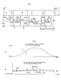
- FIG. 3 is a diagram showing a special circuit configuration in the light-receiving signal processing system in the aforementioned rain drop detecting device 1, and FIG. 4A to FIG. 6 each show a change of a signal state in the major part.
- the photo diode PD 11 as the light-receiving element 12 has an anode connected to a ground GND and a cathode connected to one end of a resistance R21 the other end of which is connected to a power source voltage VCC of, for example, 5V in the current high pass filter circuit 20, thus being subjected to reverse bias.
- VCC power source voltage
- the current high pass filter circuit 20 is provided with the aforementioned resistance R21 and a condenser C21 one end of which is connected to a connecting point between the other end of the resistance R21 and the cathode of the photo diode PD11.
- the current high pass filter circuit 20 is configured such that the other end of the condenser C21 is connected to a reverse input terminal of an operational amplifier OPAMP31, which will be described later, of the latter current to voltage conversion circuit 30 , thus operating as an active current high pass filter.
- a resistance value Ra of the resistance R21 is selected with an allowance such that an electric potential difference due to direct-current current by outside light or the like flowing in the resistance does not exceed the power source voltage VCC.
- Direct-current components of the light-received current in the photo diode PD11 flow in the resistance R21, and alternate-current components thereof flow in the condenser C21.
- a flow direction of each component follows a flow in the photo diode PD11.
- the direct-current and alternate-current components respectively flow from the resistance R21 to the photo diode PD11 (cathode thereof) and from the latter current to voltage conversion circuit 30 via the condenser C21 to the photo diode PD11 (cathode thereof).
- the current to voltage conversion circuit 30 is provided with an operational amplifier OPAMP31, and an reverse input terminal (-)thereof is connected to the condenser C21 in the current high pass filter circuit 20 as described above.
- a resistance R33 is connected between an output terminal and the reverse input terminal of the operational amplifier OPAMP31, and the current outputted from the output terminal flows out through the resistance R33 to the current high pass filter circuit 20.
- An electric potential difference (amplitude) ⁇ Vp by the current flowing in the resistance R33 includes pulse optical elements ⁇ Vp - sig and undershoots ⁇ Vp - under.
- the voltage offset unit 31 is configured of a resistance R31 connected to a non-reverse input terminal (+) of the operational amplifier OPAMP31 and the power source voltage VCC, and likewise a resistance R32 connected between the non-reverse input terminal and the ground GND.
- a voltage obtained by adding the aforementioned electric potential difference ⁇ Vp to an offset voltage Vos1 by voltage dividing between the resistance R31 and the resistance R32 becomes an output voltage of the current to voltage conversion circuit 30.
- the offset voltage Vos1 is set such that a ratio between the resistance R31 and the resistance R32 is equivalent to a ratio between the pulse optical element ⁇ Vp - sig and the undershoot ⁇ Vp - under in the electric potential difference ⁇ Vp. For example, when the pulse optical element ⁇ Vp - sig and the undershoot ⁇ Vp - under are equal in amounts, the offset voltage Vos1 is set to 2.5V when the power source voltage VCC is 5V.
- a current to voltage conversion rate of the current to voltage conversion circuit 30 is set to select a resistance value of the resistance R33 such that the output voltage is not saturated in the pulse optical element ⁇ Vp - sig and the undershoot ⁇ Vp - under.
- the electric potential difference ⁇ Vp is widened to 2.5V when the power source voltage VCC is 5V.
- a condenser may be connected in parallel to the resistance R33 to form a low pass filter. In this case, a cutting-off frequency of the low pass filter is set higher than a cutting-off frequency of the prior current high pass filter circuit 20.
- the output voltage in the current to voltage conversion circuit 30 is outputted to the voltage high pass filter circuit 40.
- the voltage high pass filter circuit 40 is formed of a condenser C41, a resistance R41 provided between the condenser C41 and the power source voltage VCC, and a resistance R42 provided between the condenser C41 and the ground GND.
- the voltage high pass filter circuit 40 further removes the outside optical element from the output voltage (light-receiving signal) of the current to voltage conversion circuit 30.
- a primary high pass voltage filter is configured by the combined resistance value Ra and the capacity value Ca.
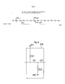
- the light-received current flowing in the photo diode PD11 is, as shown in FIG. 4A , formed in such a manner that pulse optical elements Fp by the light-emitting element 11 are superimposed on outside optical elements Fg, and an amplitude level of the outside optical element Fg is remarkably larger as compared to that of the pulse optical element Fp, and the output voltage which passes through the current high pass filter circuit 20 and is then converted in the current to voltage conversion circuit 30 is, as shown in Fig. 4B , formed such that the undershoot ⁇ Vp - under is included, but the pulse optical element ⁇ Vp - sig increases to largely attenuate a change of outside optical elements (low frequency alternate-current components ⁇ Vg - ac).
- the light-receiving signal after the current to voltage conversion is offset by the offset voltage Vos1 by a voltage dividing ratio between the resistances R31 and R32, which is inputted to the non-reverse input terminal of the operational amplifier OPAMP31.
- the offset unit 41 additionally attached to the voltage high pass filter circuit 40 is configured by in series connecting the resistance R41 connected to the power source voltage VCC to the resistance R42 connected to the ground GND, that is, the resistances R41 and R42 are used in common to the voltage high pass filter circuit 40.
- An output voltage (light-receiving signal) offset to a side of a high voltage from the GND electric potential is obtained in a connecting point between the resistances R41 and R42 as shown in Fig. 5A .
- An offset voltage Vos2 of the output voltage is set with an allowance by adjusting the voltage dividing ratio between the resistances R41 and R42 in such a manner that a lower end (minimum value) of the undershoot ⁇ Vp - under is equal to or more than the minimum input voltage (for example, 0V)of the operational amplifier OPAMP51 in the peak hold circuit 50.
- the peak hold circuit 50 is provided with the operational amplifier OPAMP51, and the output voltage of the voltage high pass filter circuit 40 is inputted as a light-receiving signal to a non-reverse input terminal of the operational amplifier OPAMP51.
- a diode D51 and a condenser C51 are in series provided in that order between an output terminal of the operational amplifier OPAMP51 and the ground GND, and a connecting point between the diode D51 and the condenser C51 is connected to a reverse input terminal of the operational amplifier OPAMP51.
- a resistance R51 and a switch element S51 are in series provided between the connecting point between the diode D51 and the condenser C51, and the ground GND.
- the switch element S51 turns on at the time of receiving a peak hold release signal from a peak hold release signal control terminal p1 in the control unit 70, for discharging the condenser C51.
- the switch element S51 turns off at the time of receiving OFF of the peak hold release signal, and the condenser C51 is charged with the input voltage of the peak hold circuit 50.
- the voltage to be inputted from the voltage high pass filter circuit 40 to the peak hold circuit 50 is a voltage obtained by adding the offset voltage Vos2 by the voltage offset unit 41 to the pulse optical element ⁇ Vp - sig and the undershoot ⁇ Vp - under, but a peak hold release signal from the control unit 70 changes from ON (release of peak hold) to OFF (hold of peal hold) at timing of a pulse light-emitting start in synchronization with timing of the pulse light-emitting of the light-emitting element 11 controlled by the control unit 70,and changes from OFF (hold of peak hold) to ON (release of peak hold) after a predetermined time for which at least the undershoot ⁇ Vp - under is attenuated elapses.
- the control unit 70 is provided with other control terminals such as a terminal of sending a control signal to the light-emitting element drive unit 15, which are omitted in illustration.
- the non-reverse amplifying circuit 60 is provided with an operational amplifier OPAMP61, wherein a non-reverse input terminal thereof is connected to a connecting point between the diode D51 and the condenser C51, and the output of the peak hold circuit 50 is inputted to the operational amplifier OPAMP61.
- Resistances R61 and R62 are in series provided between the power source voltage VCC and the ground GND, and a connecting point between both the resistances is connected to a reverse input terminal of the operational amplifier OPAMP61, as well as a resistance R63 is connected between the reverse input terminal and the output terminal.
- the condenser C51 in the peak hold circuit 50 is connected to the non-reverse input terminal of the operational amplifier OPAMP61, and an input impedance of the non-reverse input terminal is high. Therefore the peak of the voltage can be held without flowing out the current from the condenser C51 to the non-reverse amplifying circuit 60, therefore without loads to the peak hold circuit 50.
- an offset calibrating unit 61 can be realized by adjusting a voltage dividing ratio between the resistances R61 and R62 and can absorb the offset voltage Vos2 by the resistances R41 and R42 in the prior offset unit 41, outputting an amplifying peak value ⁇ Vsig as an amplitude value from the GND electric potential from the output terminal of the operational amplifier OPAMP61 as shown in Fig. 6 .
- an amplitude level can be also made to a desired level in such a manner as to be attenuated within an output voltage range of the operational amplifier OPAMP61 without distortion.
- the output terminal of the operational amplifier OPAMP61 is connected to an A/D input terminal p2 of the control unit 70.
- the control unit 70 peak values of the light-receiving signal are sampled by predetermined intervals, which are subjected to A/D conversion to generate rain drop information.
- a rainfall situation is determined based upon the rain drop information to send a wiper control signal for controlling ON/OFF of a wiper or a wiper speed from a wiper control signal output terminal p3 to a wiper control device (not shown) or the like.
- At least one of the current high pass filter circuit 20 and the voltage high pass filter circuit 40 corresponds to a high pass filter circuit in the invention defined in claim 1
- the voltage high pass filter circuit 40 corresponds to a high pass filter circuit in the invention defined in claim 3 and a latter high pass filter circuit in the invention defined in claim 5
- the current high pass filter circuit 20 corresponds to a high pass filter circuit in the invention defined in claim 4 and a former high pass filter circuit in the invention defined in claim 5.
- the control unit 70 corresponds to state determining means.
- the voltage offset unit 40 corresponds to offset means in the invention defined in claim 2, and particularly the resistance R41 corresponds to a first resistance, and the resistance R42 corresponds to a second resistance.
- the non-reverse input terminal of the operational amplifier OPAMP51 corresponds to a light-receiving signal input terminal of the peak hold circuit.
- the voltage offset unit 31 corresponds to offset means in the invention defined in claim 4, and particularly the resistance R31 corresponds to a first resistance, and the resistance R32 corresponds to a second resistance.
- the non-reverse input terminal of the operational amplifier OPAMP31 corresponds to a reference signal input terminal of the current to voltage conversion circuit.
- the resistance R61 corresponds to a third resistance in the invention defined in claim 6, and the resistance R62 corresponds to a fourth resistance.
- the rain drop detecting device 1 including the light-emitting element 11 for emitting pulse light toward a detection surface S on a surface of the window shield W for a vehicle, and the photo diode PD11 as the light-receiving element 12 for receiving light reflected on the detection surface, detecting rain drops based upon output of the photo diode PD11, comprises the current to voltage conversion circuit 30 for converting the light-receiving signal, in which the outside optical element is superimposed on the pulse optical element outputted from the photo diode PD11, from current to voltage, the current high pass filter circuit 20 and the voltage high pass filter circuit 40 for extracting the pulse optical element from the light-receiving signal, the peak hold circuit 50 for peak-holding the light-receiving signal having passed through the current to voltage conversion circuit 30 and each of the high pass filter circuits 20 and 40 to output the peak value ⁇ Vp/h - sig, the non-reverse amplifying circuit 60 for amplifying the output of the
- the current to voltage conversion rate in the current to voltage conversion circuit 30 can be increased without saturation by the outside light, and the amplifying circuit having a high amplifying rate required prior to the peak hold circuit 50 becomes unnecessary. Therefore there exists no adverse effect of the circuit noises which can be generated in the amplifying circuit having the high amplifying rate.
- the voltage high pass filter circuit 40 is also provided after the current to voltage conversion circuit 30, so that a reduction of the outside optical element can be furthermore ensured.
- the voltage offset unit 41 in the voltage high pass filter circuit 40 and the offset calibrating unit 61 in the non-reverse amplifying circuit 60 are provided, and even if the light-receiving signal (pulse optical elements ⁇ Vp - sig) inputted to the peak hold circuit 50 is offset in voltage, the offset voltage can be absorbed. Therefore the following components which are conventionally required prior to the input to the peak hold circuit 50 become unnecessary.
- the high pass filter biased to the ground voltage as a negative power source of the peak hold circuit the blocking circuit such as the analogue switch for preventing the undershoot generated at the time the pulse signal passes through the high pass filter from being equal to or less than the minimum input voltage (equal to or less than the ground electric potential) of the peak hold circuit, and the buffer circuit or the amplifying circuit in a case where the high pass filter and the blocking circuit are not connected directly to the peak hold circuit become unnecessary.
- the non-reverse amplifying circuit 60 after the peak hold circuit 50, the voltage buffer which is conventionally required after the peak hold circuit 50 becomes unnecessary.
- the offset calibrating unit 61 in the non-reverse amplifying circuit 60 can once more offset the inputted voltage in a direction of absorbing the offset by the voltage offset unit 41 in the voltage high pass filter circuit 40 to amplify the output of the peak hold circuit 50, a peak signal value can be outputted as an amplifying amplitude value from the ground.
- the voltage offset unit 41 in the voltage high pass filter circuit 40 is configured such that the resistance R41 connected to the power source voltage and the resistance R42 connected to the ground are in series arranged and the connecting point to the resistance R41 is connected to the non-reverse input terminal of the operational amplifier OPAMP51 in the peak hold circuit 50. Therefore the configuration of the voltage offset unit 41 is simpler as compared to the configuration of blocking input of the undershoot to the peak hold circuit 50 using an expensive analogue switch, and can be commonly used also as filter constant formation of the voltage high pass filter circuit 40. Accordingly even as compared to the conventional filter biased to the ground electric potential, the voltage offset unit 41 can be inexpensively configured by adding a single resistance.
- the voltage high pass filter circuit 40 is provided after the current to voltage conversion circuit 30 in addition to the current high pass filter circuit 20, but when the low frequency alternate-current components ⁇ Vg - ac appearing in FIG. 4B disappear, and as shown in FIG. 7 , the outside optical elements are sufficiently removed, the voltage high pass filter circuit 40 and the offset unit 41 may be omitted.
- the offset voltage Vos1 by the offset unit 31 instead of the offset unit 41, particularly the lower end (minimum value) of the undershoot in the output voltage in the current to voltage conversion circuit 30 may be set to a value equal to or more than the minimum input voltage of the operational amplifier OPAMP51 in the peak hold circuit 50.
- the current high pass filter circuit 20 in the present embodiment is shown as the primary high pass filter, but, as shown in Fig.8 , when there is provided a current high pass filter circuit 20A in which a condenser C22 is provided after the condenser C21 (in a side of the current to voltage conversion circuit 30) and a resistance R22 is provided between a connecting point between the condenser C21 and the condenser C22, and the ground GND, a secondary high pass filter can be configured with ease and at low costs, and performance for attenuating outside optical elements as noises improves corresponding to the order increase.
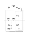
- the voltage high pass filter circuit 40 in the present embodiment is also shown as the primary high pass filter, but, as shown in Fig.9 , when there is provided a voltage high pass filter circuit 40A in which a condenser C42 is provided between the connecting point between the resistance R41 and the resistance R42, and the condenser C41, and a resistance R43 is provided between a connecting point between the condenser C41 and a condenser C42, and the ground GND, a secondary high pass filter can be likewise configured with ease and at low costs, and performance for attenuating outside optical elements as noises further improves corresponding to the order increase.
- the voltage high pass filter circuit 40 (40A) is configured of a first- or more-order of the high pass filter, a band pass filter having a low pass filter of a cutting-off frequency larger than that of the high pass filter may be used.
- the present invention is not limited thereto, but can be applied to various types of state detecting devices for detecting a state of the detection target based upon a light-receiving signal under circumstances where outside light exists.
Landscapes
- Engineering & Computer Science (AREA)
- Physics & Mathematics (AREA)
- General Physics & Mathematics (AREA)
- Spectroscopy & Molecular Physics (AREA)
- Power Engineering (AREA)
- Automation & Control Theory (AREA)
- Mechanical Engineering (AREA)
- Amplifiers (AREA)
- Investigating Or Analysing Materials By Optical Means (AREA)
Applications Claiming Priority (1)
| Application Number | Priority Date | Filing Date | Title |
|---|---|---|---|
| JP2011157366A JP5832802B2 (ja) | 2011-07-19 | 2011-07-19 | 状態検出装置 |
Publications (3)
| Publication Number | Publication Date |
|---|---|
| EP2549248A2 true EP2549248A2 (de) | 2013-01-23 |
| EP2549248A3 EP2549248A3 (de) | 2013-07-31 |
| EP2549248B1 EP2549248B1 (de) | 2019-04-17 |
Family
ID=46982318
Family Applications (1)
| Application Number | Title | Priority Date | Filing Date |
|---|---|---|---|
| EP12005076.0A Not-in-force EP2549248B1 (de) | 2011-07-19 | 2012-07-09 | Regentropfen-Messgerät mit einer Zustandserfassungseinheit |
Country Status (3)
| Country | Link |
|---|---|
| EP (1) | EP2549248B1 (de) |
| JP (1) | JP5832802B2 (de) |
| HU (1) | HUE045454T2 (de) |
Cited By (4)
| Publication number | Priority date | Publication date | Assignee | Title |
|---|---|---|---|---|
| FR3007856A1 (fr) * | 2013-06-27 | 2015-01-02 | Continental Automotive France | Dispositif de traitement d'un signal provenant d'une thermopile et procede associe |
| EP3128346A3 (de) * | 2015-08-05 | 2017-02-15 | Ricoh Company Ltd. | Detektor von gepulstem licht, objektdetektor, sensor; bewegliche vorrichtung und verfahren zur detektion von gepulstem licht |
| CN106716150A (zh) * | 2014-07-25 | 2017-05-24 | 美国亚德诺半导体公司 | 模式切换的电路结构 |
| US10056868B2 (en) | 2013-04-25 | 2018-08-21 | Analog Devices, Inc. | Four-stage circuit architecture for detecting pulsed signals |
Citations (1)
| Publication number | Priority date | Publication date | Assignee | Title |
|---|---|---|---|---|
| JP2004340712A (ja) | 2003-05-15 | 2004-12-02 | Nippon Sheet Glass Co Ltd | レインセンサ用の信号検出回路および信号検出方法 |
Family Cites Families (2)
| Publication number | Priority date | Publication date | Assignee | Title |
|---|---|---|---|---|
| JP4055327B2 (ja) * | 2000-03-31 | 2008-03-05 | 日本ビクター株式会社 | パケット信号受信回路 |
| KR20060015608A (ko) * | 2003-05-15 | 2006-02-17 | 나이루스 가부시키가이샤 | 레인 센서용 신호 검출회로 및 신호 검출방법 |
-
2011
- 2011-07-19 JP JP2011157366A patent/JP5832802B2/ja active Active
-
2012
- 2012-07-09 EP EP12005076.0A patent/EP2549248B1/de not_active Not-in-force
- 2012-07-09 HU HUE12005076A patent/HUE045454T2/hu unknown
Patent Citations (1)
| Publication number | Priority date | Publication date | Assignee | Title |
|---|---|---|---|---|
| JP2004340712A (ja) | 2003-05-15 | 2004-12-02 | Nippon Sheet Glass Co Ltd | レインセンサ用の信号検出回路および信号検出方法 |
Cited By (6)
| Publication number | Priority date | Publication date | Assignee | Title |
|---|---|---|---|---|
| US10056868B2 (en) | 2013-04-25 | 2018-08-21 | Analog Devices, Inc. | Four-stage circuit architecture for detecting pulsed signals |
| FR3007856A1 (fr) * | 2013-06-27 | 2015-01-02 | Continental Automotive France | Dispositif de traitement d'un signal provenant d'une thermopile et procede associe |
| CN106716150A (zh) * | 2014-07-25 | 2017-05-24 | 美国亚德诺半导体公司 | 模式切换的电路结构 |
| EP3172581A4 (de) * | 2014-07-25 | 2018-04-18 | Analog Devices, Inc. | Schaltungsarchitektur für wahlschalter |
| CN106716150B (zh) * | 2014-07-25 | 2021-01-19 | 美国亚德诺半导体公司 | 模式切换的电路结构 |
| EP3128346A3 (de) * | 2015-08-05 | 2017-02-15 | Ricoh Company Ltd. | Detektor von gepulstem licht, objektdetektor, sensor; bewegliche vorrichtung und verfahren zur detektion von gepulstem licht |
Also Published As
| Publication number | Publication date |
|---|---|
| JP5832802B2 (ja) | 2015-12-16 |
| EP2549248B1 (de) | 2019-04-17 |
| HUE045454T2 (hu) | 2019-12-30 |
| JP2013024618A (ja) | 2013-02-04 |
| EP2549248A3 (de) | 2013-07-31 |
Similar Documents
| Publication | Publication Date | Title |
|---|---|---|
| US8207488B2 (en) | Photodetector circuit | |
| JP5889152B2 (ja) | 受光回路、レーザレーダ | |
| EP2549248B1 (de) | Regentropfen-Messgerät mit einer Zustandserfassungseinheit | |
| JP4590974B2 (ja) | 光受信回路 | |
| CN103457673B (zh) | 提高apd光接收机饱和光功率的方法和装置 | |
| EP2226940B1 (de) | Lichtempfangserkennungsschaltung | |
| US20090245807A1 (en) | Optical power monitoring circuit, optical transceiver, optical module, optical receiver, amplifier circuit, and integrated circuit | |
| US5517351A (en) | Optical receiver apparatus | |
| KR100324880B1 (ko) | 피크홀드회로및이를구비하는적외선통신장치 | |
| JP3999055B2 (ja) | 信号検出処理回路 | |
| TW200939628A (en) | Photoelectric sensor | |
| JP4760312B2 (ja) | 光受信器 | |
| US7531783B2 (en) | Variable gain constant bandwidth trans-impedance amplifier for fiber optic rate sensor | |
| JP3925442B2 (ja) | レインセンサ | |
| JP2009139159A (ja) | 雨滴検出装置 | |
| JP2007303887A (ja) | 雨滴検知装置 | |
| CN222234437U (zh) | 一种泄放电路和激光雷达 | |
| US12143111B2 (en) | Fast signal response circuit with hysteresis control | |
| JP2009047587A (ja) | センサ信号増幅装置 | |
| JP5058105B2 (ja) | 光信号送受信器 | |
| JP3188106B2 (ja) | 光電式煙感知器 | |
| JP3878192B2 (ja) | 赤外線通信装置 | |
| KR970003453Y1 (ko) | 카메라의 자동 거리 측정장치 | |
| CN119172005A (zh) | 一种自动增益控制模块、信号处理芯片和光接收器 | |
| WO2004102167A1 (ja) | レインセンサ用の信号検出回路および信号検出方法 |
Legal Events
| Date | Code | Title | Description |
|---|---|---|---|
| PUAI | Public reference made under article 153(3) epc to a published international application that has entered the european phase |
Free format text: ORIGINAL CODE: 0009012 |
|
| AK | Designated contracting states |
Kind code of ref document: A2 Designated state(s): AL AT BE BG CH CY CZ DE DK EE ES FI FR GB GR HR HU IE IS IT LI LT LU LV MC MK MT NL NO PL PT RO RS SE SI SK SM TR |
|
| AX | Request for extension of the european patent |
Extension state: BA ME |
|
| PUAL | Search report despatched |
Free format text: ORIGINAL CODE: 0009013 |
|
| AK | Designated contracting states |
Kind code of ref document: A3 Designated state(s): AL AT BE BG CH CY CZ DE DK EE ES FI FR GB GR HR HU IE IS IT LI LT LU LV MC MK MT NL NO PL PT RO RS SE SI SK SM TR |
|
| AX | Request for extension of the european patent |
Extension state: BA ME |
|
| RIC1 | Information provided on ipc code assigned before grant |
Ipc: G01J 1/18 20060101AFI20130625BHEP Ipc: G01J 1/46 20060101ALI20130625BHEP Ipc: B60S 1/08 20060101ALI20130625BHEP |
|
| 17P | Request for examination filed |
Effective date: 20131018 |
|
| RBV | Designated contracting states (corrected) |
Designated state(s): AL AT BE BG CH CY CZ DE DK EE ES FI FR GB GR HR HU IE IS IT LI LT LU LV MC MK MT NL NO PL PT RO RS SE SI SK SM TR |
|
| RAP1 | Party data changed (applicant data changed or rights of an application transferred) |
Owner name: VALEO JAPAN CO., LTD. |
|
| GRAP | Despatch of communication of intention to grant a patent |
Free format text: ORIGINAL CODE: EPIDOSNIGR1 |
|
| STAA | Information on the status of an ep patent application or granted ep patent |
Free format text: STATUS: GRANT OF PATENT IS INTENDED |
|
| INTG | Intention to grant announced |
Effective date: 20180626 |
|
| RIN1 | Information on inventor provided before grant (corrected) |
Inventor name: TOUJU, MASAAKI Inventor name: OHATA, TOMOYUKI |
|
| GRAS | Grant fee paid |
Free format text: ORIGINAL CODE: EPIDOSNIGR3 |
|
| GRAA | (expected) grant |
Free format text: ORIGINAL CODE: 0009210 |
|
| STAA | Information on the status of an ep patent application or granted ep patent |
Free format text: STATUS: THE PATENT HAS BEEN GRANTED |
|
| AK | Designated contracting states |
Kind code of ref document: B1 Designated state(s): AL AT BE BG CH CY CZ DE DK EE ES FI FR GB GR HR HU IE IS IT LI LT LU LV MC MK MT NL NO PL PT RO RS SE SI SK SM TR |
|
| REG | Reference to a national code |
Ref country code: GB Ref legal event code: FG4D |
|
| REG | Reference to a national code |
Ref country code: CH Ref legal event code: EP |
|
| REG | Reference to a national code |
Ref country code: DE Ref legal event code: R096 Ref document number: 602012059002 Country of ref document: DE |
|
| REG | Reference to a national code |
Ref country code: AT Ref legal event code: REF Ref document number: 1122067 Country of ref document: AT Kind code of ref document: T Effective date: 20190515 Ref country code: IE Ref legal event code: FG4D |
|
| REG | Reference to a national code |
Ref country code: NL Ref legal event code: MP Effective date: 20190417 |
|
| REG | Reference to a national code |
Ref country code: LT Ref legal event code: MG4D |
|
| PG25 | Lapsed in a contracting state [announced via postgrant information from national office to epo] |
Ref country code: NL Free format text: LAPSE BECAUSE OF FAILURE TO SUBMIT A TRANSLATION OF THE DESCRIPTION OR TO PAY THE FEE WITHIN THE PRESCRIBED TIME-LIMIT Effective date: 20190417 |
|
| PG25 | Lapsed in a contracting state [announced via postgrant information from national office to epo] |
Ref country code: ES Free format text: LAPSE BECAUSE OF FAILURE TO SUBMIT A TRANSLATION OF THE DESCRIPTION OR TO PAY THE FEE WITHIN THE PRESCRIBED TIME-LIMIT Effective date: 20190417 Ref country code: LT Free format text: LAPSE BECAUSE OF FAILURE TO SUBMIT A TRANSLATION OF THE DESCRIPTION OR TO PAY THE FEE WITHIN THE PRESCRIBED TIME-LIMIT Effective date: 20190417 Ref country code: FI Free format text: LAPSE BECAUSE OF FAILURE TO SUBMIT A TRANSLATION OF THE DESCRIPTION OR TO PAY THE FEE WITHIN THE PRESCRIBED TIME-LIMIT Effective date: 20190417 Ref country code: HR Free format text: LAPSE BECAUSE OF FAILURE TO SUBMIT A TRANSLATION OF THE DESCRIPTION OR TO PAY THE FEE WITHIN THE PRESCRIBED TIME-LIMIT Effective date: 20190417 Ref country code: NO Free format text: LAPSE BECAUSE OF FAILURE TO SUBMIT A TRANSLATION OF THE DESCRIPTION OR TO PAY THE FEE WITHIN THE PRESCRIBED TIME-LIMIT Effective date: 20190717 Ref country code: AL Free format text: LAPSE BECAUSE OF FAILURE TO SUBMIT A TRANSLATION OF THE DESCRIPTION OR TO PAY THE FEE WITHIN THE PRESCRIBED TIME-LIMIT Effective date: 20190417 Ref country code: PT Free format text: LAPSE BECAUSE OF FAILURE TO SUBMIT A TRANSLATION OF THE DESCRIPTION OR TO PAY THE FEE WITHIN THE PRESCRIBED TIME-LIMIT Effective date: 20190817 Ref country code: SE Free format text: LAPSE BECAUSE OF FAILURE TO SUBMIT A TRANSLATION OF THE DESCRIPTION OR TO PAY THE FEE WITHIN THE PRESCRIBED TIME-LIMIT Effective date: 20190417 |
|
| PG25 | Lapsed in a contracting state [announced via postgrant information from national office to epo] |
Ref country code: RS Free format text: LAPSE BECAUSE OF FAILURE TO SUBMIT A TRANSLATION OF THE DESCRIPTION OR TO PAY THE FEE WITHIN THE PRESCRIBED TIME-LIMIT Effective date: 20190417 Ref country code: LV Free format text: LAPSE BECAUSE OF FAILURE TO SUBMIT A TRANSLATION OF THE DESCRIPTION OR TO PAY THE FEE WITHIN THE PRESCRIBED TIME-LIMIT Effective date: 20190417 Ref country code: GR Free format text: LAPSE BECAUSE OF FAILURE TO SUBMIT A TRANSLATION OF THE DESCRIPTION OR TO PAY THE FEE WITHIN THE PRESCRIBED TIME-LIMIT Effective date: 20190718 Ref country code: PL Free format text: LAPSE BECAUSE OF FAILURE TO SUBMIT A TRANSLATION OF THE DESCRIPTION OR TO PAY THE FEE WITHIN THE PRESCRIBED TIME-LIMIT Effective date: 20190417 Ref country code: BG Free format text: LAPSE BECAUSE OF FAILURE TO SUBMIT A TRANSLATION OF THE DESCRIPTION OR TO PAY THE FEE WITHIN THE PRESCRIBED TIME-LIMIT Effective date: 20190717 |
|
| REG | Reference to a national code |
Ref country code: AT Ref legal event code: MK05 Ref document number: 1122067 Country of ref document: AT Kind code of ref document: T Effective date: 20190417 |
|
| REG | Reference to a national code |
Ref country code: HU Ref legal event code: AG4A Ref document number: E045454 Country of ref document: HU |
|
| PG25 | Lapsed in a contracting state [announced via postgrant information from national office to epo] |
Ref country code: IS Free format text: LAPSE BECAUSE OF FAILURE TO SUBMIT A TRANSLATION OF THE DESCRIPTION OR TO PAY THE FEE WITHIN THE PRESCRIBED TIME-LIMIT Effective date: 20190817 |
|
| REG | Reference to a national code |
Ref country code: DE Ref legal event code: R097 Ref document number: 602012059002 Country of ref document: DE |
|
| PG25 | Lapsed in a contracting state [announced via postgrant information from national office to epo] |
Ref country code: CZ Free format text: LAPSE BECAUSE OF FAILURE TO SUBMIT A TRANSLATION OF THE DESCRIPTION OR TO PAY THE FEE WITHIN THE PRESCRIBED TIME-LIMIT Effective date: 20190417 Ref country code: RO Free format text: LAPSE BECAUSE OF FAILURE TO SUBMIT A TRANSLATION OF THE DESCRIPTION OR TO PAY THE FEE WITHIN THE PRESCRIBED TIME-LIMIT Effective date: 20190417 Ref country code: EE Free format text: LAPSE BECAUSE OF FAILURE TO SUBMIT A TRANSLATION OF THE DESCRIPTION OR TO PAY THE FEE WITHIN THE PRESCRIBED TIME-LIMIT Effective date: 20190417 Ref country code: SK Free format text: LAPSE BECAUSE OF FAILURE TO SUBMIT A TRANSLATION OF THE DESCRIPTION OR TO PAY THE FEE WITHIN THE PRESCRIBED TIME-LIMIT Effective date: 20190417 Ref country code: AT Free format text: LAPSE BECAUSE OF FAILURE TO SUBMIT A TRANSLATION OF THE DESCRIPTION OR TO PAY THE FEE WITHIN THE PRESCRIBED TIME-LIMIT Effective date: 20190417 Ref country code: DK Free format text: LAPSE BECAUSE OF FAILURE TO SUBMIT A TRANSLATION OF THE DESCRIPTION OR TO PAY THE FEE WITHIN THE PRESCRIBED TIME-LIMIT Effective date: 20190417 |
|
| PLBE | No opposition filed within time limit |
Free format text: ORIGINAL CODE: 0009261 |
|
| STAA | Information on the status of an ep patent application or granted ep patent |
Free format text: STATUS: NO OPPOSITION FILED WITHIN TIME LIMIT |
|
| PG25 | Lapsed in a contracting state [announced via postgrant information from national office to epo] |
Ref country code: MC Free format text: LAPSE BECAUSE OF FAILURE TO SUBMIT A TRANSLATION OF THE DESCRIPTION OR TO PAY THE FEE WITHIN THE PRESCRIBED TIME-LIMIT Effective date: 20190417 Ref country code: SM Free format text: LAPSE BECAUSE OF FAILURE TO SUBMIT A TRANSLATION OF THE DESCRIPTION OR TO PAY THE FEE WITHIN THE PRESCRIBED TIME-LIMIT Effective date: 20190417 Ref country code: IT Free format text: LAPSE BECAUSE OF FAILURE TO SUBMIT A TRANSLATION OF THE DESCRIPTION OR TO PAY THE FEE WITHIN THE PRESCRIBED TIME-LIMIT Effective date: 20190417 |
|
| REG | Reference to a national code |
Ref country code: CH Ref legal event code: PL |
|
| 26N | No opposition filed |
Effective date: 20200120 |
|
| PG25 | Lapsed in a contracting state [announced via postgrant information from national office to epo] |
Ref country code: TR Free format text: LAPSE BECAUSE OF FAILURE TO SUBMIT A TRANSLATION OF THE DESCRIPTION OR TO PAY THE FEE WITHIN THE PRESCRIBED TIME-LIMIT Effective date: 20190417 |
|
| REG | Reference to a national code |
Ref country code: BE Ref legal event code: MM Effective date: 20190731 |
|
| PG25 | Lapsed in a contracting state [announced via postgrant information from national office to epo] |
Ref country code: LI Free format text: LAPSE BECAUSE OF NON-PAYMENT OF DUE FEES Effective date: 20190731 Ref country code: BE Free format text: LAPSE BECAUSE OF NON-PAYMENT OF DUE FEES Effective date: 20190731 Ref country code: CH Free format text: LAPSE BECAUSE OF NON-PAYMENT OF DUE FEES Effective date: 20190731 Ref country code: SI Free format text: LAPSE BECAUSE OF FAILURE TO SUBMIT A TRANSLATION OF THE DESCRIPTION OR TO PAY THE FEE WITHIN THE PRESCRIBED TIME-LIMIT Effective date: 20190417 Ref country code: LU Free format text: LAPSE BECAUSE OF NON-PAYMENT OF DUE FEES Effective date: 20190709 |
|
| PG25 | Lapsed in a contracting state [announced via postgrant information from national office to epo] |
Ref country code: IE Free format text: LAPSE BECAUSE OF NON-PAYMENT OF DUE FEES Effective date: 20190709 |
|
| PG25 | Lapsed in a contracting state [announced via postgrant information from national office to epo] |
Ref country code: CY Free format text: LAPSE BECAUSE OF FAILURE TO SUBMIT A TRANSLATION OF THE DESCRIPTION OR TO PAY THE FEE WITHIN THE PRESCRIBED TIME-LIMIT Effective date: 20190417 |
|
| PG25 | Lapsed in a contracting state [announced via postgrant information from national office to epo] |
Ref country code: MT Free format text: LAPSE BECAUSE OF FAILURE TO SUBMIT A TRANSLATION OF THE DESCRIPTION OR TO PAY THE FEE WITHIN THE PRESCRIBED TIME-LIMIT Effective date: 20190417 |
|
| PGFP | Annual fee paid to national office [announced via postgrant information from national office to epo] |
Ref country code: FR Payment date: 20210722 Year of fee payment: 10 |
|
| PGFP | Annual fee paid to national office [announced via postgrant information from national office to epo] |
Ref country code: HU Payment date: 20210705 Year of fee payment: 10 Ref country code: DE Payment date: 20210724 Year of fee payment: 10 Ref country code: GB Payment date: 20210722 Year of fee payment: 10 |
|
| PG25 | Lapsed in a contracting state [announced via postgrant information from national office to epo] |
Ref country code: MK Free format text: LAPSE BECAUSE OF FAILURE TO SUBMIT A TRANSLATION OF THE DESCRIPTION OR TO PAY THE FEE WITHIN THE PRESCRIBED TIME-LIMIT Effective date: 20190417 |
|
| REG | Reference to a national code |
Ref country code: DE Ref legal event code: R119 Ref document number: 602012059002 Country of ref document: DE |
|
| GBPC | Gb: european patent ceased through non-payment of renewal fee |
Effective date: 20220709 |
|
| PG25 | Lapsed in a contracting state [announced via postgrant information from national office to epo] |
Ref country code: FR Free format text: LAPSE BECAUSE OF NON-PAYMENT OF DUE FEES Effective date: 20220731 |
|
| PG25 | Lapsed in a contracting state [announced via postgrant information from national office to epo] |
Ref country code: HU Free format text: LAPSE BECAUSE OF NON-PAYMENT OF DUE FEES Effective date: 20220710 Ref country code: GB Free format text: LAPSE BECAUSE OF NON-PAYMENT OF DUE FEES Effective date: 20220709 Ref country code: DE Free format text: LAPSE BECAUSE OF NON-PAYMENT OF DUE FEES Effective date: 20230201 |
|
| P01 | Opt-out of the competence of the unified patent court (upc) registered |
Effective date: 20230528 |