EP2549745A2 - Verfahren und Bildsensor mit Pixelstruktur zur Erfassung von Tiefen- und Farbbildern - Google Patents
Verfahren und Bildsensor mit Pixelstruktur zur Erfassung von Tiefen- und Farbbildern Download PDFInfo
- Publication number
- EP2549745A2 EP2549745A2 EP12155769A EP12155769A EP2549745A2 EP 2549745 A2 EP2549745 A2 EP 2549745A2 EP 12155769 A EP12155769 A EP 12155769A EP 12155769 A EP12155769 A EP 12155769A EP 2549745 A2 EP2549745 A2 EP 2549745A2
- Authority
- EP
- European Patent Office
- Prior art keywords
- pixels
- image sensor
- pixel
- node
- image
- Prior art date
- Legal status (The legal status is an assumption and is not a legal conclusion. Google has not performed a legal analysis and makes no representation as to the accuracy of the status listed.)
- Withdrawn
Links
Images



Classifications
-
- H—ELECTRICITY
- H04—ELECTRIC COMMUNICATION TECHNIQUE
- H04N—PICTORIAL COMMUNICATION, e.g. TELEVISION
- H04N25/00—Circuitry of solid-state image sensors [SSIS]; Control thereof
- H04N25/70—SSIS architectures; Circuits associated therewith
- H04N25/76—Addressed sensors, e.g. MOS or CMOS sensors
- H04N25/77—Pixel circuitry, e.g. memories, A/D converters, pixel amplifiers, shared circuits or shared components
-
- H—ELECTRICITY
- H04—ELECTRIC COMMUNICATION TECHNIQUE
- H04N—PICTORIAL COMMUNICATION, e.g. TELEVISION
- H04N23/00—Cameras or camera modules comprising electronic image sensors; Control thereof
- H04N23/60—Control of cameras or camera modules
- H04N23/667—Camera operation mode switching, e.g. between still and video, sport and normal or high- and low-resolution modes
-
- H—ELECTRICITY
- H04—ELECTRIC COMMUNICATION TECHNIQUE
- H04N—PICTORIAL COMMUNICATION, e.g. TELEVISION
- H04N23/00—Cameras or camera modules comprising electronic image sensors; Control thereof
- H04N23/80—Camera processing pipelines; Components thereof
- H04N23/84—Camera processing pipelines; Components thereof for processing colour signals
-
- H—ELECTRICITY
- H04—ELECTRIC COMMUNICATION TECHNIQUE
- H04N—PICTORIAL COMMUNICATION, e.g. TELEVISION
- H04N25/00—Circuitry of solid-state image sensors [SSIS]; Control thereof
- H04N25/10—Circuitry of solid-state image sensors [SSIS]; Control thereof for transforming different wavelengths into image signals
-
- H—ELECTRICITY
- H04—ELECTRIC COMMUNICATION TECHNIQUE
- H04N—PICTORIAL COMMUNICATION, e.g. TELEVISION
- H04N25/00—Circuitry of solid-state image sensors [SSIS]; Control thereof
- H04N25/10—Circuitry of solid-state image sensors [SSIS]; Control thereof for transforming different wavelengths into image signals
- H04N25/11—Arrangement of colour filter arrays [CFA]; Filter mosaics
- H04N25/13—Arrangement of colour filter arrays [CFA]; Filter mosaics characterised by the spectral characteristics of the filter elements
- H04N25/134—Arrangement of colour filter arrays [CFA]; Filter mosaics characterised by the spectral characteristics of the filter elements based on three different wavelength filter elements
-
- H—ELECTRICITY
- H04—ELECTRIC COMMUNICATION TECHNIQUE
- H04N—PICTORIAL COMMUNICATION, e.g. TELEVISION
- H04N25/00—Circuitry of solid-state image sensors [SSIS]; Control thereof
- H04N25/40—Extracting pixel data from image sensors by controlling scanning circuits, e.g. by modifying the number of pixels sampled or to be sampled
- H04N25/46—Extracting pixel data from image sensors by controlling scanning circuits, e.g. by modifying the number of pixels sampled or to be sampled by combining or binning pixels
-
- H—ELECTRICITY
- H04—ELECTRIC COMMUNICATION TECHNIQUE
- H04N—PICTORIAL COMMUNICATION, e.g. TELEVISION
- H04N25/00—Circuitry of solid-state image sensors [SSIS]; Control thereof
- H04N25/70—SSIS architectures; Circuits associated therewith
-
- H—ELECTRICITY
- H04—ELECTRIC COMMUNICATION TECHNIQUE
- H04N—PICTORIAL COMMUNICATION, e.g. TELEVISION
- H04N25/00—Circuitry of solid-state image sensors [SSIS]; Control thereof
- H04N25/70—SSIS architectures; Circuits associated therewith
- H04N25/703—SSIS architectures incorporating pixels for producing signals other than image signals
- H04N25/705—Pixels for depth measurement, e.g. RGBZ
-
- H—ELECTRICITY
- H04—ELECTRIC COMMUNICATION TECHNIQUE
- H04N—PICTORIAL COMMUNICATION, e.g. TELEVISION
- H04N25/00—Circuitry of solid-state image sensors [SSIS]; Control thereof
- H04N25/70—SSIS architectures; Circuits associated therewith
- H04N25/76—Addressed sensors, e.g. MOS or CMOS sensors
- H04N25/77—Pixel circuitry, e.g. memories, A/D converters, pixel amplifiers, shared circuits or shared components
- H04N25/778—Pixel circuitry, e.g. memories, A/D converters, pixel amplifiers, shared circuits or shared components comprising amplifiers shared between a plurality of pixels, i.e. at least one part of the amplifier must be on the sensor array itself
-
- H—ELECTRICITY
- H04—ELECTRIC COMMUNICATION TECHNIQUE
- H04N—PICTORIAL COMMUNICATION, e.g. TELEVISION
- H04N25/00—Circuitry of solid-state image sensors [SSIS]; Control thereof
- H04N25/70—SSIS architectures; Circuits associated therewith
- H04N25/76—Addressed sensors, e.g. MOS or CMOS sensors
- H04N25/78—Readout circuits for addressed sensors, e.g. output amplifiers or A/D converters
-
- H—ELECTRICITY
- H10—SEMICONDUCTOR DEVICES; ELECTRIC SOLID-STATE DEVICES NOT OTHERWISE PROVIDED FOR
- H10F—INORGANIC SEMICONDUCTOR DEVICES SENSITIVE TO INFRARED RADIATION, LIGHT, ELECTROMAGNETIC RADIATION OF SHORTER WAVELENGTH OR CORPUSCULAR RADIATION
- H10F39/00—Integrated devices, or assemblies of multiple devices, comprising at least one element covered by group H10F30/00, e.g. radiation detectors comprising photodiode arrays
- H10F39/80—Constructional details of image sensors
- H10F39/802—Geometry or disposition of elements in pixels, e.g. address-lines or gate electrodes
-
- H—ELECTRICITY
- H10—SEMICONDUCTOR DEVICES; ELECTRIC SOLID-STATE DEVICES NOT OTHERWISE PROVIDED FOR
- H10F—INORGANIC SEMICONDUCTOR DEVICES SENSITIVE TO INFRARED RADIATION, LIGHT, ELECTROMAGNETIC RADIATION OF SHORTER WAVELENGTH OR CORPUSCULAR RADIATION
- H10F39/00—Integrated devices, or assemblies of multiple devices, comprising at least one element covered by group H10F30/00, e.g. radiation detectors comprising photodiode arrays
- H10F39/80—Constructional details of image sensors
- H10F39/813—Electronic components shared by multiple pixels, e.g. one amplifier shared by two pixels
Definitions
- Example embodiments of the following description relate to an image sensor having a pixel structure for capturing a depth image and a color image, and more particularly, to an image sensor having a pixel structure including pixels sharing a floating diffusion (FD) node.
- FD floating diffusion
- a conventional image capturing apparatus extracts only a color image of an object and therefore is limited in obtaining a 3D image.
- a time of flight (TOF) method has been used to extract a depth image of an object.
- the TOF method determines a travel time of light by emitting light onto the object and detecting the light reflected from the object.
- Pixels generally used in a depth camera for extracting the depth image range in size between approximately 30 micrometers ( ⁇ m) and 40 ⁇ m.
- Pixels generally used in a color camera for extracting the color image range in size between approximately 1.4 ⁇ m and 3.6 ⁇ m.
- a pixel size needs to be reduced for extraction of both the depth image and the color image.
- a size of a photodiode included in a pixel is also reduced. As a result, sensitivity of the photodiode is reduced.
- an image sensor including an N-number of pixels, wherein at least some of the N-number of pixels share a floating diffusion (FD) node and optionally also a readout circuit, which is preferably connected to the FD node, with at least one of the other pixels of the N-number of pixels.
- FD floating diffusion
- an image sensor wherein at least some of the N-number of pixels share a FD node with a first neighboring pixel located on the left and share a second FD node with a second FD node with a second neighboring pixel located on the right.
- an image sensor wherein at least some of the N-number of pixels share a first FD node with a first neighboring pixel, the FD node being located below the first neighboring pixel, and shares a second FD node with a second neighboring pixel, the second FD node being located above the second neighboring pixel.
- an image sensor including a control circuit, wherein the control circuit generates first binning images by binning output images output from a unit number of pixels in a charge domain, and generates second binning images by binning the first binning images in an analog domain.
- a method for capturing a depth image and a color image including providing an N-number of pixels; sharing readout and FD nodes between pixels of the N-number of pixels; and providing a color mode to capture a color image and a depth mode to capture a depth image, wherein both modes are executed using a same pixel structure.
- the fill factor may be increased through sharing of a transistor for readout and floating diffusion (FD) nodes among pixels. Therefore, a sense of color and accuracy of depth may be maintained.
- FD floating diffusion
- a pixel in a depth mode, is firstly binned in a charge domain and secondly binned in an analog domain. As a result, accuracy of depth may be increased.
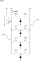
- FIG. 1 illustrates a structure of a 4-shared color/depth pixel according to example embodiments.
- an image sensor includes four pixels, each of which includes two transfer gates. Also, each pixel may connect three transistors, that is, a reset (RST) transistor, a select (SEL) transistor, and a source follower (SF) transistor.
- RST reset
- SEL select
- SF source follower
- a first pixel includes transfer gates Tx0 and TX1 and a second pixel includes transfer gates TX2 and TX3.
- a third pixel includes transfer gates TX4 and TX5 while a fourth pixel includes transfer gates TX6 and TX7. Accordingly, the image sensor shown in FIG. 1 represents a 4 x 1 pixel structure.
- the four pixels aforementioned share a single readout circuit 102.
- the pixels are selected according to a signal input through the SEL transistor.
- the four pixels aforementioned share a floating diffusion (FD) node 101.
- An operation of the image sensor of FIG. 1 will be described in detail with reference to FIG. 2 .
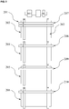
- FIG. 2 illustrates a layout of the pixel structure of FIG. 1 .
- a first pixel 203 includes a transfer gate 0 and a transfer gate 1.
- a second pixel 204 includes a transfer gate 2 and a transfer gate 3.
- a third pixel 205 includes a transfer gate 4 and a transfer gate 5.
- a fourth pixel 206 includes a transfer gate 6 and a transfer gate 7.
- transfer gates TX 2n+1 receive input signals. That is, all of the transfer gates 0 to 7 are operated. In this case, since the transfer gates TX 2n+1 are shared by the first pixel 203, the second pixel 204, the third pixel 250, and the fourth pixel 206, all those pixels are controlled by the same signal. That is, since the transfer gates 1, 3, 5 and 7 are operable by the same signal, the first pixel 203, the second pixel 204, the third pixel 250, and the fourth pixel 206 may share the same row.
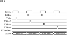
- FIG. 3 illustrates a color mode of a pixel structure, according to example embodiments.
- a signal being inputted to a pixel represents a rolling shutter operation.
- transfer gates are connected, and the charges collected to a photodiode of each pixel are transferred to a FD node.
- FIG. 4 illustrates a depth mode of the pixel structure, according to example embodiments.
- a light emitting diode (LED) signal and a transfer gate (TX) signal are synchronized in the depth mode.
- the TX signal is globally operated. Charges are integrated during an integration time that outputs a signal modulated by an LED. After that, the charges are read out row by row in a similar manner to the color mode.
- FIG. 5 illustrates a 4 x 2 pixel structure that shares an FD node 501 with a neighboring pixel, according to example embodiments.
- the image sensor having the 4 x 2 pixel structure shown in FIG. 5 includes two 4 x 1 pixel structures of FIG. 1 .
- the image sensor of FIG. 5 may include four pixels as in FIG. 1 , the four pixels sharing an RST transistor, a SEL transistor, and an SF transistor.
- the fill factor may be increased.
- signals being applied to the FD node 501 may be read out simultaneously.
- the image sensor may select a green (G) column or a red/blue (R/B) column according to the control of a transfer gate.
- G green
- R/B red/blue
- the image sensor may be converted to an 8-shared structure where eight pixels share the FD node 501.
- FIG. 6 illustrates a first layout of a 4 x 4 pixel structure that shares an FD node with a neighboring pixel in a color mode, according to example embodiments.
- FIG. 6 shows a transfer direction of charges in an image sensor having the 4 x 4 pixel structure in the color mode.
- transfer gates may be divided into gates denoted by 0 to 7 and gates denoted by D0 to D4. Only the transfer gates 0 to 7 are operated in the color mode.
- a dotted line in FIG. 6 denotes FD nodes in a shared state.
- the reason for transferring the charges of the pixels of the row 4n and row 4n+1 to the FD nodes in different directions is to minimize a mismatch between a Gr pixel and a Gb pixel.
- the image sensor may have alternate charge transfer directions to transfer the charges of the Gr pixel and the Gb pixel to the same FD node. That is, according to the image sensor shown in FIG. 6 , sensitivity of the image sensor may be increased through sharing of the FD nodes. Additionally, a sense of color may be increased since an R/B color channel and a G color channel are separated.
- the image sensor may bind FD nodes of the green pixels located in different columns into one by controlling operations of transfer gates according to the row.
- FIG. 7 illustrates a first layout of a 4 x 4 pixel structure that shares an FD node with a neighboring pixel in a depth mode, according to example embodiments.
- transfer gates 0 to 7 and transfer gates D0 to D4 all operate. Therefore, all sensors included in the image sensor are simultaneously operated so that depth images are collected.
- FIG. 8 illustrates a second layout of a 4 x 4 pixel structure that shares an FD node with a neighboring pixel in a color mode, according to example embodiments.
- the 4 x 4 pixel structure of FIG. 8 is different from the 4 x 4 pixel structure of FIG. 6 in that charges are transferred in a lateral direction in FIG. 6 , whereas, charges are transferred in a vertical direction in FIG. 8 .
- the operating principles are the same. That is, transfer gates 0 to 7 are operated in the color mode.
- a dotted line denotes FD nodes being shared.
- transfer gates 2 and 3 When transfer gates 2 and 3 are operated to read out pixel values corresponding to a next row, that is, row 4n+1, charges of each green pixel are transferred to the FD node located above, while charges of each blue pixel are transferred to the FD node located below.
- FD nodes of green pixels located on different columns may be bound into one.
- FIG. 9 illustrates a second layout of a 4 x 4 pixel structure that shares an FD node with a neighboring pixel in a depth mode, according to example embodiments.
- transfer gates 0 to 7 and transfer gates D0 to D7 are all operated. In this case, all sensors included in the image sensor are operated so that depth images are collected.
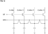
- FIG. 10 illustrates a circuit for pixel binning in an analog domain according to example embodiments.
- the circuit shown in FIG. 10 operates as follows.
- FIG. 11 illustrates hierarchical binning where pixel binning in a charge domain and pixel binning in an analog domain are sequentially performed.
- images sensed by pixels 1101, 1102, 1103, and 1104 are first binned in the charge domain and indicated by one "Z."
- an image sensor having a 4 x 1 pixel structure may be set as one unit and indicated by one "Z.”
- the image sensor having the 4 x 1 pixel structure may show a total of four "Zs”.
- an image sensor having a 4 x 2 pixel structure may be set as one unit.
- the four "Zs" derived from the image sensor as one unit may be binned and indicated by one large "Z.” That is, an image indicated in the analog domain shows that the images shown in 16 pixels in the charge domain are all binned. Since a circuit operation for the analog binning has been described in detail with reference to FIG. 10 , a detailed description will be omitted for conciseness.
- the methods according to the above-described example embodiments may be recorded in non-transitory computer-readable media including program instructions to implement various operations embodied by a computer.
- the media may also include, alone or in combination with the program instructions, data files, data structures, and the like.
- the program instructions recorded on the media may be those specially designed and constructed for the purposes of the example embodiments, or they may be of the kind well-known and available to those having skill in the computer software arts.
- the embodiments can be implemented in computing hardware (computing apparatus) and/or software, such as (in a non-limiting example) any computer that can store, retrieve, process and/or output data and/or communicate with other computers.
- the results produced can be displayed on a display of the computing hardware.
- a program/software implementing the embodiments may be recorded on non-transitory computer-readable media comprising computer-readable recording media.
- the computer-readable recording media include a magnetic recording apparatus, an optical disk, a magneto-optical disk, and/or a semiconductor memory (for example, RAM, ROM, etc.).
- Examples of the magnetic recording apparatus include a hard disk device (HDD), a flexible disk (FD), and a magnetic tape (MT).
- Examples of the optical disk include a DVD (Digital Versatile Disc), a DVD-RAM, a CD-ROM (Compact Disc - Read Only Memory), and a CD-R (Recordable)/RW.
- the image sensor may include at least one processor to execute at least one of the above-described units and methods.
Landscapes
- Engineering & Computer Science (AREA)
- Multimedia (AREA)
- Signal Processing (AREA)
- Physics & Mathematics (AREA)
- Spectroscopy & Molecular Physics (AREA)
- Solid State Image Pick-Up Elements (AREA)
- Transforming Light Signals Into Electric Signals (AREA)
Applications Claiming Priority (1)
| Application Number | Priority Date | Filing Date | Title |
|---|---|---|---|
| KR1020110073022A KR20130011692A (ko) | 2011-07-22 | 2011-07-22 | 깊이 영상과 컬러 영상을 획득하는 픽셀 구조를 가진 이미지 센서 |
Publications (2)
| Publication Number | Publication Date |
|---|---|
| EP2549745A2 true EP2549745A2 (de) | 2013-01-23 |
| EP2549745A3 EP2549745A3 (de) | 2013-10-09 |
Family
ID=45592254
Family Applications (1)
| Application Number | Title | Priority Date | Filing Date |
|---|---|---|---|
| EP12155769.8A Withdrawn EP2549745A3 (de) | 2011-07-22 | 2012-02-16 | Verfahren und Bildsensor mit Pixelstruktur zur Erfassung von Tiefen- und Farbbildern |
Country Status (3)
| Country | Link |
|---|---|
| US (1) | US20130021441A1 (de) |
| EP (1) | EP2549745A3 (de) |
| KR (1) | KR20130011692A (de) |
Cited By (3)
| Publication number | Priority date | Publication date | Assignee | Title |
|---|---|---|---|---|
| FR3005205A1 (fr) * | 2013-04-26 | 2014-10-31 | St Microelectronics Grenoble 2 | Capteur d'image a gain de conversion multiple |
| FR3042912A1 (fr) * | 2015-10-26 | 2017-04-28 | Stmicroelectronics (Grenoble 2) Sas | Capteur d'images a grande gamme dynamique |
| US9998693B2 (en) | 2016-02-26 | 2018-06-12 | Stmicroelectronics (Grenoble 2) Sas | Image sensor adapted to blinking sources |
Families Citing this family (27)
| Publication number | Priority date | Publication date | Assignee | Title |
|---|---|---|---|---|
| US9398287B2 (en) | 2013-02-28 | 2016-07-19 | Google Technology Holdings LLC | Context-based depth sensor control |
| US9407837B2 (en) * | 2013-02-28 | 2016-08-02 | Google Inc. | Depth sensor using modulated light projector and image sensor with color and IR sensing |
| JP6176062B2 (ja) * | 2013-11-06 | 2017-08-09 | ソニー株式会社 | 固体撮像装置およびその駆動方法、並びに電子機器 |
| JP6373027B2 (ja) * | 2014-03-24 | 2018-08-15 | キヤノン株式会社 | 撮像装置 |
| US9729809B2 (en) * | 2014-07-11 | 2017-08-08 | Semiconductor Energy Laboratory Co., Ltd. | Semiconductor device and driving method of semiconductor device or electronic device |
| US9883130B2 (en) | 2015-03-09 | 2018-01-30 | Rambus Inc. | Image sensor with feedthrough-compensated charge-binned readout |
| US9686486B2 (en) * | 2015-05-27 | 2017-06-20 | Semiconductor Components Industries, Llc | Multi-resolution pixel architecture with shared floating diffusion nodes |
| EP3333893B1 (de) | 2015-08-04 | 2020-02-19 | Panasonic Intellectual Property Management Co., Ltd. | Festkörperbildgebungsvorrichtung |
| US9983709B2 (en) | 2015-11-02 | 2018-05-29 | Oculus Vr, Llc | Eye tracking using structured light |
| US10241569B2 (en) | 2015-12-08 | 2019-03-26 | Facebook Technologies, Llc | Focus adjustment method for a virtual reality headset |
| US10025060B2 (en) | 2015-12-08 | 2018-07-17 | Oculus Vr, Llc | Focus adjusting virtual reality headset |
| US10445860B2 (en) | 2015-12-08 | 2019-10-15 | Facebook Technologies, Llc | Autofocus virtual reality headset |
| US9858672B2 (en) | 2016-01-15 | 2018-01-02 | Oculus Vr, Llc | Depth mapping using structured light and time of flight |
| US11106276B2 (en) | 2016-03-11 | 2021-08-31 | Facebook Technologies, Llc | Focus adjusting headset |
| US10379356B2 (en) | 2016-04-07 | 2019-08-13 | Facebook Technologies, Llc | Accommodation based optical correction |
| US10313609B2 (en) | 2016-04-14 | 2019-06-04 | Qualcomm Incorporated | Image sensors having pixel-binning with configurable shared floating diffusion |
| US10313610B2 (en) * | 2016-04-14 | 2019-06-04 | Qualcomm Incorporated | Image sensors with dynamic pixel binning |
| DE102016208347B4 (de) * | 2016-05-13 | 2017-12-21 | Infineon Technologies Ag | Optische Sensorvorrichtung und Verfahren zum Betreiben eines Laufzeitsensors |
| US10429647B2 (en) | 2016-06-10 | 2019-10-01 | Facebook Technologies, Llc | Focus adjusting virtual reality headset |
| US10025384B1 (en) | 2017-01-06 | 2018-07-17 | Oculus Vr, Llc | Eye tracking architecture for common structured light and time-of-flight framework |
| US10310598B2 (en) | 2017-01-17 | 2019-06-04 | Facebook Technologies, Llc | Varifocal head-mounted display including modular air spaced optical assembly |
| US10154254B2 (en) | 2017-01-17 | 2018-12-11 | Facebook Technologies, Llc | Time-of-flight depth sensing for eye tracking |
| US10679366B1 (en) | 2017-01-30 | 2020-06-09 | Facebook Technologies, Llc | High speed computational tracking sensor |
| CN111034177B (zh) * | 2017-09-14 | 2022-06-28 | 新唐科技日本株式会社 | 固体摄像装置以及具备该固体摄像装置的摄像装置 |
| WO2020234645A1 (en) * | 2019-05-21 | 2020-11-26 | Sony Semiconductor Solutions Corporation | Dual mode imaging devices |
| US11272132B2 (en) * | 2019-06-07 | 2022-03-08 | Pacific Biosciences Of California, Inc. | Temporal differential active pixel sensor |
| CN116567443B (zh) * | 2023-04-28 | 2026-04-28 | 上海炬佑智能科技有限公司 | 可编程、多功能的、多分辨率2d/3dcmos图像传感器及其操作方法 |
Family Cites Families (17)
| Publication number | Priority date | Publication date | Assignee | Title |
|---|---|---|---|---|
| JP3906202B2 (ja) * | 2003-12-15 | 2007-04-18 | 株式会社東芝 | 固体撮像装置およびそれを利用した撮像システム |
| JP4665422B2 (ja) * | 2004-04-02 | 2011-04-06 | ソニー株式会社 | 撮像装置 |
| JP2007180152A (ja) * | 2005-12-27 | 2007-07-12 | Canon Inc | 測定方法及び装置、露光装置、並びに、デバイス製造方法 |
| KR100790583B1 (ko) * | 2006-10-16 | 2008-01-02 | (주) 픽셀플러스 | 씨모스 이미지 센서 공유 픽셀 |
| KR100823173B1 (ko) * | 2007-02-16 | 2008-04-21 | 삼성전자주식회사 | 씨모스 이미지 센서 |
| US7964929B2 (en) * | 2007-08-23 | 2011-06-21 | Aptina Imaging Corporation | Method and apparatus providing imager pixels with shared pixel components |
| JP5026951B2 (ja) * | 2007-12-26 | 2012-09-19 | オリンパスイメージング株式会社 | 撮像素子の駆動装置、撮像素子の駆動方法、撮像装置、及び撮像素子 |
| KR100913797B1 (ko) * | 2008-01-30 | 2009-08-26 | (주) 픽셀플러스 | Cmos 이미지 센서 |
| KR101467509B1 (ko) * | 2008-07-25 | 2014-12-01 | 삼성전자주식회사 | 이미지 센서 및 이미지 센서 동작 방법 |
| US20100253769A1 (en) * | 2008-09-04 | 2010-10-07 | Laser Light Engines | Optical System and Assembly Method |
| TWI433307B (zh) * | 2008-10-22 | 2014-04-01 | Sony Corp | 固態影像感測器、其驅動方法、成像裝置及電子器件 |
| US20100309340A1 (en) * | 2009-06-03 | 2010-12-09 | Border John N | Image sensor having global and rolling shutter processes for respective sets of pixels of a pixel array |
| JP5644177B2 (ja) * | 2010-05-07 | 2014-12-24 | ソニー株式会社 | 固体撮像装置、および、その製造方法、電子機器 |
| JP2011238311A (ja) * | 2010-05-10 | 2011-11-24 | Hitachi Consumer Electronics Co Ltd | 光情報再生装置、光情報記録装置および光情報記録再生装置 |
| KR20120119279A (ko) * | 2011-04-21 | 2012-10-31 | 삼성전자주식회사 | 픽셀 어레이 및 이를 포함하는 3차원 이미지 센서 |
| US9129172B2 (en) * | 2011-06-20 | 2015-09-08 | Metrologic Instruments, Inc. | Indicia reading terminal with color frame processing |
| US9229096B2 (en) * | 2011-07-27 | 2016-01-05 | Semiconductor Components Industries, Llc | Time-of-flight imaging systems |
-
2011
- 2011-07-22 KR KR1020110073022A patent/KR20130011692A/ko not_active Ceased
-
2012
- 2012-01-23 US US13/356,384 patent/US20130021441A1/en not_active Abandoned
- 2012-02-16 EP EP12155769.8A patent/EP2549745A3/de not_active Withdrawn
Non-Patent Citations (1)
| Title |
|---|
| None |
Cited By (4)
| Publication number | Priority date | Publication date | Assignee | Title |
|---|---|---|---|---|
| FR3005205A1 (fr) * | 2013-04-26 | 2014-10-31 | St Microelectronics Grenoble 2 | Capteur d'image a gain de conversion multiple |
| FR3042912A1 (fr) * | 2015-10-26 | 2017-04-28 | Stmicroelectronics (Grenoble 2) Sas | Capteur d'images a grande gamme dynamique |
| US10009558B2 (en) | 2015-10-26 | 2018-06-26 | Stmicroelectronics (Grenoble 2) Sas | High dynamic range image sensor |
| US9998693B2 (en) | 2016-02-26 | 2018-06-12 | Stmicroelectronics (Grenoble 2) Sas | Image sensor adapted to blinking sources |
Also Published As
| Publication number | Publication date |
|---|---|
| EP2549745A3 (de) | 2013-10-09 |
| US20130021441A1 (en) | 2013-01-24 |
| KR20130011692A (ko) | 2013-01-30 |
Similar Documents
| Publication | Publication Date | Title |
|---|---|---|
| EP2549745A2 (de) | Verfahren und Bildsensor mit Pixelstruktur zur Erfassung von Tiefen- und Farbbildern | |
| US11477409B2 (en) | Image processing device and mobile computing device having the same | |
| US9544513B2 (en) | Image sensor having pixel architecture for capturing depth image and color image | |
| KR102288164B1 (ko) | 이미지 처리 장치와 이를 포함하는 모바일 컴퓨팅 장치 | |
| KR101977711B1 (ko) | 깊이 센서, 이의 이미지 캡쳐 방법, 및 상기 깊이 센서를 포함하는 이미지 처리 시스템 | |
| CN110072069B (zh) | 图像传感器 | |
| JP5521854B2 (ja) | 撮像装置及び画像入力装置 | |
| US20170146657A1 (en) | Imaging sensor with shared pixel readout circuitry | |
| WO2013183266A2 (en) | Semiconductor device and sensing system | |
| DE102013111706A1 (de) | Verfahren und Vorrichtungen zum Erkennen von Bewegung von Objekten und zugehörige Systeme | |
| US11658193B2 (en) | Image sensor | |
| US10542231B2 (en) | Method of driving image pickup device, image pickup device, image pickup system | |
| US10277807B2 (en) | Image device and method for memory-to-memory image processing | |
| KR20200115779A (ko) | 이미징 장치 및 이미지 센서 | |
| KR20200010769A (ko) | 이미지 센서 | |
| KR20200108132A (ko) | 이미지 센서 | |
| KR102709791B1 (ko) | 이미지 센서 | |
| CN105611257A (zh) | 成像方法、图像传感器、成像装置及电子装置 | |
| US11532654B2 (en) | Image sensor | |
| KR102497658B1 (ko) | 이미지 센서 | |
| KR20260013619A (ko) | 이미지 센서 장치 및 그것의 동작 방법 | |
| CN107948551A (zh) | 图像传感器中的固定模式噪声减少 |
Legal Events
| Date | Code | Title | Description |
|---|---|---|---|
| PUAI | Public reference made under article 153(3) epc to a published international application that has entered the european phase |
Free format text: ORIGINAL CODE: 0009012 |
|
| AK | Designated contracting states |
Kind code of ref document: A2 Designated state(s): AL AT BE BG CH CY CZ DE DK EE ES FI FR GB GR HR HU IE IS IT LI LT LU LV MC MK MT NL NO PL PT RO RS SE SI SK SM TR |
|
| AX | Request for extension of the european patent |
Extension state: BA ME |
|
| PUAL | Search report despatched |
Free format text: ORIGINAL CODE: 0009013 |
|
| AK | Designated contracting states |
Kind code of ref document: A3 Designated state(s): AL AT BE BG CH CY CZ DE DK EE ES FI FR GB GR HR HU IE IS IT LI LT LU LV MC MK MT NL NO PL PT RO RS SE SI SK SM TR |
|
| AX | Request for extension of the european patent |
Extension state: BA ME |
|
| RIC1 | Information provided on ipc code assigned before grant |
Ipc: H04N 5/3745 20110101AFI20130903BHEP |
|
| 17P | Request for examination filed |
Effective date: 20140327 |
|
| RBV | Designated contracting states (corrected) |
Designated state(s): AL AT BE BG CH CY CZ DE DK EE ES FI FR GB GR HR HU IE IS IT LI LT LU LV MC MK MT NL NO PL PT RO RS SE SI SK SM TR |
|
| 17Q | First examination report despatched |
Effective date: 20161122 |
|
| STAA | Information on the status of an ep patent application or granted ep patent |
Free format text: STATUS: THE APPLICATION IS DEEMED TO BE WITHDRAWN |
|
| 18D | Application deemed to be withdrawn |
Effective date: 20170404 |