EP2551720A1 - Système d'imagerie pour l'imagerie d'objets a mouvement rapide - Google Patents
Système d'imagerie pour l'imagerie d'objets a mouvement rapide Download PDFInfo
- Publication number
- EP2551720A1 EP2551720A1 EP12177430A EP12177430A EP2551720A1 EP 2551720 A1 EP2551720 A1 EP 2551720A1 EP 12177430 A EP12177430 A EP 12177430A EP 12177430 A EP12177430 A EP 12177430A EP 2551720 A1 EP2551720 A1 EP 2551720A1
- Authority
- EP
- European Patent Office
- Prior art keywords
- shutter
- imaging system
- control unit
- imaging
- detector
- Prior art date
- Legal status (The legal status is an assumption and is not a legal conclusion. Google has not performed a legal analysis and makes no representation as to the accuracy of the status listed.)
- Granted
Links
- 238000003384 imaging method Methods 0.000 title claims abstract description 51
- 238000012545 processing Methods 0.000 claims abstract description 6
- 238000011144 upstream manufacturing Methods 0.000 claims abstract description 6
- 230000005540 biological transmission Effects 0.000 claims abstract description 3
- 230000033001 locomotion Effects 0.000 claims description 39
- 230000010287 polarization Effects 0.000 claims description 15
- 230000000737 periodic effect Effects 0.000 claims description 14
- 238000001514 detection method Methods 0.000 claims description 11
- 239000004973 liquid crystal related substance Substances 0.000 claims description 7
- 238000007493 shaping process Methods 0.000 claims description 2
- 238000004846 x-ray emission Methods 0.000 claims description 2
- 238000000034 method Methods 0.000 description 17
- 235000012431 wafers Nutrition 0.000 description 11
- 238000004458 analytical method Methods 0.000 description 6
- 230000005284 excitation Effects 0.000 description 5
- 239000011295 pitch Substances 0.000 description 5
- 230000002123 temporal effect Effects 0.000 description 5
- 101100460147 Sarcophaga bullata NEMS gene Proteins 0.000 description 4
- 230000005855 radiation Effects 0.000 description 4
- 238000005070 sampling Methods 0.000 description 4
- 238000012546 transfer Methods 0.000 description 4
- XUIMIQQOPSSXEZ-UHFFFAOYSA-N Silicon Chemical compound [Si] XUIMIQQOPSSXEZ-UHFFFAOYSA-N 0.000 description 3
- 238000005286 illumination Methods 0.000 description 3
- 229910052710 silicon Inorganic materials 0.000 description 3
- 239000010703 silicon Substances 0.000 description 3
- 238000012512 characterization method Methods 0.000 description 2
- 239000000463 material Substances 0.000 description 2
- 239000002070 nanowire Substances 0.000 description 2
- 230000003287 optical effect Effects 0.000 description 2
- 230000001360 synchronised effect Effects 0.000 description 2
- 238000003325 tomography Methods 0.000 description 2
- 229920000297 Rayon Polymers 0.000 description 1
- 238000006243 chemical reaction Methods 0.000 description 1
- 238000001493 electron microscopy Methods 0.000 description 1
- 230000001788 irregular Effects 0.000 description 1
- 230000007257 malfunction Effects 0.000 description 1
- 238000005259 measurement Methods 0.000 description 1
- 230000010355 oscillation Effects 0.000 description 1
- 239000002245 particle Substances 0.000 description 1
- 238000002601 radiography Methods 0.000 description 1
- 239000002964 rayon Substances 0.000 description 1
- 238000011160 research Methods 0.000 description 1
- 230000000630 rising effect Effects 0.000 description 1
- 230000007704 transition Effects 0.000 description 1
Images


Classifications
-
- G—PHYSICS
- G03—PHOTOGRAPHY; CINEMATOGRAPHY; ANALOGOUS TECHNIQUES USING WAVES OTHER THAN OPTICAL WAVES; ELECTROGRAPHY; HOLOGRAPHY
- G03B—APPARATUS OR ARRANGEMENTS FOR TAKING PHOTOGRAPHS OR FOR PROJECTING OR VIEWING THEM; APPARATUS OR ARRANGEMENTS EMPLOYING ANALOGOUS TECHNIQUES USING WAVES OTHER THAN OPTICAL WAVES; ACCESSORIES THEREFOR
- G03B42/00—Obtaining records using waves other than optical waves; Visualisation of such records by using optical means
- G03B42/02—Obtaining records using waves other than optical waves; Visualisation of such records by using optical means using X-rays
-
- G—PHYSICS
- G01—MEASURING; TESTING
- G01N—INVESTIGATING OR ANALYSING MATERIALS BY DETERMINING THEIR CHEMICAL OR PHYSICAL PROPERTIES
- G01N23/00—Investigating or analysing materials by the use of wave or particle radiation, e.g. X-rays or neutrons, not covered by groups G01N3/00 – G01N17/00, G01N21/00 or G01N22/00
- G01N23/02—Investigating or analysing materials by the use of wave or particle radiation, e.g. X-rays or neutrons, not covered by groups G01N3/00 – G01N17/00, G01N21/00 or G01N22/00 by transmitting the radiation through the material
- G01N23/04—Investigating or analysing materials by the use of wave or particle radiation, e.g. X-rays or neutrons, not covered by groups G01N3/00 – G01N17/00, G01N21/00 or G01N22/00 by transmitting the radiation through the material and forming images of the material
-
- G—PHYSICS
- G01—MEASURING; TESTING
- G01T—MEASUREMENT OF NUCLEAR OR X-RADIATION
- G01T1/00—Measuring X-radiation, gamma radiation, corpuscular radiation, or cosmic radiation
- G01T1/29—Measurement performed on radiation beams, e.g. position or section of the beam; Measurement of spatial distribution of radiation
- G01T1/2914—Measurement of spatial distribution of radiation
- G01T1/2921—Static instruments for imaging the distribution of radioactivity in one or two dimensions; Radio-isotope cameras
- G01T1/2957—Static instruments for imaging the distribution of radioactivity in one or two dimensions; Radio-isotope cameras using channel multiplier arrays
-
- H—ELECTRICITY
- H04—ELECTRIC COMMUNICATION TECHNIQUE
- H04N—PICTORIAL COMMUNICATION, e.g. TELEVISION
- H04N5/00—Details of television systems
- H04N5/30—Transforming light or analogous information into electric information
- H04N5/32—Transforming X-rays
-
- G—PHYSICS
- G01—MEASURING; TESTING
- G01N—INVESTIGATING OR ANALYSING MATERIALS BY DETERMINING THEIR CHEMICAL OR PHYSICAL PROPERTIES
- G01N2223/00—Investigating materials by wave or particle radiation
- G01N2223/30—Accessories, mechanical or electrical features
- G01N2223/314—Accessories, mechanical or electrical features chopper
-
- G—PHYSICS
- G01—MEASURING; TESTING
- G01N—INVESTIGATING OR ANALYSING MATERIALS BY DETERMINING THEIR CHEMICAL OR PHYSICAL PROPERTIES
- G01N2223/00—Investigating materials by wave or particle radiation
- G01N2223/40—Imaging
- G01N2223/41—Imaging imaging specifically internal structure
-
- G—PHYSICS
- G01—MEASURING; TESTING
- G01N—INVESTIGATING OR ANALYSING MATERIALS BY DETERMINING THEIR CHEMICAL OR PHYSICAL PROPERTIES
- G01N2223/00—Investigating materials by wave or particle radiation
- G01N2223/60—Specific applications or type of materials
- G01N2223/611—Specific applications or type of materials patterned objects; electronic devices
Definitions
- the present invention relates to an imaging system for imaging fast-moving objects, in particular microelectromechanical systems MEMS (Microelectromechanical Systems) and nanoelectromechanical systems NEMS (Nanoelectremechanical Systems).
- MEMS Microelectromechanical Systems
- NEMS Nanoelectromechanical Systems
- MEMS and NEMS there are oscillators whose movement is periodic, it is for example RF switches or some gyroscopes. These MEMS and NEMS are so-called "buried" objects, that is to say that they are enclosed in silicon. Observation by means of electron microscopy, optics, electrical characterization or laser vibrometry does not work: the silicon protection is opaque to electrons and light photons and the electrical characterization does not provide images.
- microsystems For the sake of simplicity, MEMS or NEMS will all be referred to as microsystems.
- X-ray imaging can be used.
- X-ray imaging systems comprising an X-ray source, a shutter upstream of the object to be observed and means for detecting the rays transmitted by the object.
- the shutter is a mechanical lead shutter to completely stop X-rays outside the exposure period, however.
- the shutter is moved to interrupt or allow illumination of the object. Due to the inertia of the shutter and for mechanical reasons and stability, such shutters can not be used for microsystems operating frequencies that are between about 1 kHz and about 1 GHz.
- the object of the present invention is achieved by a system comprising an X-ray source, a scintillator screen for converting X-rays into visible radiation, a fixed detector and shutter disposed between the scintillator screen and the detector, the shutter being capable of switching from a state to a non-on state with a frequency above kHz and a shutter control unit.
- the shutter can be formed by a microchannel wafer, which offers in addition to a very high switching frequency, the advantage of amplifying the signal transmitted by the microsystem. Exposure times between 10 ns and 100 ns can be achieved.
- the shutter can be formed by a polarized liquid crystal mirror. Exposure times of 1 ms can be achieved.
- This system allows stroboscopic detection in the case of microsystems with periodic movement.
- This system also makes it possible to obtain a radiograph of the microsystem at a given instant by synchronizing the movement of the microsystem and the state of the shutter.
- the subject of the present invention is therefore an imaging system intended for imaging fast-moving objects, comprising an X-ray source, a scintillator screen, a shutter and a beam detector emitted by the shutter.
- processing unit connected to the detector, the shutter being disposed between the scintillator screen and the detector, and a support for the object to be observed disposed downstream of the X-ray source and upstream of the scintillator screen, the shutter being a shutter controllable at high frequencies, for example greater than about 1 kHz, the shutter being fixed and the transmission of the signal from the scintillator screen to the detector being controlled by electrical polarization means controlled by a unit of control, said imaging system also comprising means for actuating said object so as to move the moving part relative to the fixed part.
- the shutter comprises at least one microchannel slab.
- the shutter is formed by two microchannel slabs arranged one behind the other.
- a residual bias can be applied to one of the faces of a slab.
- control unit controls the polarization means so that they send voltage pulses at a frequency between 1Hz and 20 MHz.
- the duration of a pulse is for example between 10 ns and 100 ns.
- the shutter comprises at least one liquid crystal mirror oriented with respect to the scintillator screen and with respect to the detector so as to reflect the beam coming from the scintillator screen towards the detector when it is polarized.
- the control unit can control the polarization means so that they send the liquid crystal mirror voltage pulses at a frequency below 1kHz. For example, the duration of a pulse is of the order of 1 ms.
- the support is pivotable at a given angular pitch around an axis perpendicular to the emission axis of the X-ray source.
- the angular pitch may be variable.
- control unit can control the movement of the microsystem.
- the control unit may comprise means for shaping control signals of the object with a programmable delay, said shaped signals being used to control the polarization means.
- the detector is a charge transfer device.
- the detector is a CMOS sensor.
- the subject of the present invention is also an imaging method implementing an imaging system according to the present invention, in which the object has a periodic movement and the system is used to carry out a stroboscopic detection, to obtain multi-state images of the object.
- the present invention also relates to an imaging method using an imaging system according to the present invention, wherein the control unit controls the polarization means as a function of the signal driving the movement of the object.
- the control unit can form a control signal of the polarization means from the control signal of the object by introducing a programmable delay, the duration of the delay is modified so as to image several states of the object.
- the object can be rotated about an axis perpendicular to the X-ray emission axis so as to make images of the object in different angular positions.
- the angular pitch can be variable.
- the object imaged by the imaging method is a microelectromechanical system or a nanoelectromechanical system.
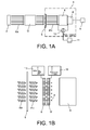
- FIG. 1A a diagrammatic representation of an imaging system according to the present invention comprising an X-ray source 2 intended to be arranged upstream of the object O to be illuminated, an X-ray collection assembly 4 designated RC in the figures, transmitted by the object O.
- the assembly 4 comprises a scintillator screen 5 converting the X-rays into visible light, a shutter 6 and an optical 8 for collecting and digital recording of the visible light transmitted by the object and the shutter and a fast electronics or unit 11 to control the shutter 6.
- the control unit 11 also controls the actuation of the microsystem.
- the actuation of the microsystem can be thermal, electrostatic or magnetic.
- the microsystems are supplied wirelessly and without contact by an external power supply, which makes it possible to eliminate the uncontrolled movements of microsystems due to rotating wires, which intervenes in the tomographic mode.
- the microsystem is powered by RF waves.
- actuating means for actuating a MEMS stress sensor are for example described in the document Wen H. Ko, Trends and Frontier of MEMS ", in Sensors and Actuators A 136 (2007) 62-67 ; the signals emitted by the sensor are also advantageously read wirelessly.
- the detection optics is for example formed by a charge-coupled device sensor or CCD sensor ("Charge-Coupled Device” in English terminology ”) provided with a scintillator which converts the electrons into visible radiation.
- CCD sensor Charge-Coupled Device
- a scintillator which converts the electrons into visible radiation.
- a direct conversion electron detector could be used, which sensors are well known to those skilled in the art and are, for example, described in the document US 7,888,781 .
- CMOS sensors which have a shorter read time than the CCD sensors could be used, but they have a poorer dynamic.
- the detection optics is connected to the processing unit 9 to which the images are sent.
- the shutter 6 is formed by a microchannel plate ("Microchannel Plate” (MCP) in English terminology).
- MCP Microchannel Plate
- a PCM is a silicon wafer pierced with a large number of microchannels, whose typical size is 10 microns. This slab is put under a voltage of several hundred volts, so that any particle incident in a microchannel and striking the wall creates a shower of electrons which are themselves accelerated and channeled along the microchannel.
- a MCP therefore makes it possible to amplify the charges.
- microchannel wafers are particularly suitable for the observation of microsystems, since the channels have a diameter of the order of 10 ⁇ m, which dimension is consistent with the observation resolution of the MEMS systems and SPRING ROLLS.
- the wafer When the wafer is polarized, it converts the visible photons (symbolized by arrows and designated PH) and UV from the scintillator screen into electrons (symbolized by arrows and designated e on the Figure 1B ) and amplifies the electronic current sent in the CCD sensor. In the absence of polarization, the wafer is opaque to these same radiations.
- the imaging system includes a voltage generator 13 for biasing the shutter.
- the voltage pulses being of the order of 700 V to 1000 V.
- control unit polarizes the wafer 6 by a voltage between 700 V and 1100 V for very short times ⁇ of the order of 10 ns to 100 ns, ⁇ being the exposure time, controlling the time image acquisition.
- a residual polarization of the order of 100V may be applied to one of the faces of the wafer to eliminate the charges created by the optical radiation in the wafer during the shutter phases.
- This image acquisition can be done at a very slow rate, for example at a frequency of the order of 1 Hz, up to fast frequencies of 2 - 20 MHz, which corresponds to f ⁇ 1 / 2 ⁇ .
- the microchannel wafer has the advantage of amplifying the electronic current sent to the sensor.
- this acquisition frequency is not necessarily regular and can be controlled by an external generator.
- the shutter is formed of two microchannel wafers in series, each amplifying the input signal, thereby improving the gain.
- the upstream slab is biased by the pulse generator 13 and a Residual polarization is applied to the downstream slab by means 15.
- the two slabs form a single shutter.
- the shutter 106 is formed by a polarized liquid crystal mirror.
- the visible image sent by the scintillator screen is reflected or not by the mirror towards the CCD sensor.
- the minimum exposure time may be of the order of 1 ms.
- the CCD receives directly photons, not electrons.
- it is a conventional type CCD sensor with a photoactive region that converts the visible photons into electrons, then the created charges are read and the image is formed. This sensor is well known to those skilled in the art and is for example described in the document US 4,996,413 .
- This imaging system is therefore particularly interesting in the case of microsystems with slow movement.
- the read times of the CCD sensors are very long.
- stroboscopy is used.
- the shutter is controlled in tension so as to acquire an X-ray to different states of the microsystem.
- the time between two pulses is at least equal to the reading and recording time of the CCD sensor.
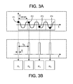
- FIG 3A the position of a microsystem that one wishes to observe as a function of time can be graphically represented.
- the points P1 to P4 correspond to the instants of the movement during a period that one wishes to observe.
- R1 to R4 correspond to the radiographs taken at these times P1 to P4.
- each pulse corresponds to a moment P1 to P4 of the movement and the duration of the pulse represents the temporal resolution of the images.
- the reading and recording of the sensor takes place between two pulses. Since the movement is periodic, one can, by recording images over several periods, obtain a film of the periodic movement of the microsystem.
- T p of the pulses applied to the shutter is: T p ⁇ T microphone + ⁇ , is T p ⁇ 50 , 01 s .
- the acquisition method makes it possible to sample the movement of the microsystem every 10 ⁇ s.
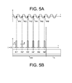
- FIG. 5A a graph showing the excitation signal applied to the microsystem as a function of time can be seen.
- the points P1 'to P6' represent the moments that one wishes to observe.
- R1 'to R6' correspond to the X-rays taken at these times P1 'to P6'.
- This method links the excitation signal of the microsystem and the shutter.
- the signal that drives the microsystem is used to control the shutter.
- the control unit transmits the signal driving the microsystem and formats this signal by introducing a programmable delay ⁇ which makes it possible to fix the instant and therefore the state of the microsystem that one wishes to observe.
- the duration ⁇ is determined during which shutter illuminates the CCD sensor.
- the signal thus transformed is sent to the voltage generator.
- the control signal, in the form of voltage pulses, of the shutter formed on the basis of the control signal of the microsystem the delay ⁇ between the beginning of the excitation signal of the system and the point P1 can be represented. to detect and the duration ⁇ of illumination of the CCD sensor.
- This configuration makes it possible to acquire a radiograph of the microsystem in a given state.
- the delay ⁇ is modified.
- the time between 2 pulses can then be much shorter than the reading and recording time t R of the CCD sensor. Choosing the shutter release time ⁇ allows you to adjust the temporal resolution of the images.
- the system is associated with a tomography detection technique, the system then comprises a support for the object to be observed which is mobile while rotating about an axis and able to move the object at a given angle so as to modify the point of view that has the CCD sensor of the microsystem.
- the images obtained at each angle of view are made by stroboscopic detection or by synchronization between the movement of the microsystem and the control of the shutter.
- the media is controlled by a CPU that rotates the media when all images from one point of view have been taken.
- the microsystem is positioned on the support, the initial angle of rotation ⁇ is equal to 0.
- n is the number of images per period of the microsystem, which has the initial value 1.
- T micro is the period of the microsystem.
- ⁇ is the exposure time
- t is the time.
- the microsystem is operated.
- a voltage pulse is sent to the shutter for a time ⁇ .
- the CDD sensor plays and the image is recorded.
- step 500 If the answer is negative (step 500), the system waits until the condition of step 400 is verified (step 600).
- n is increased by 1 (step 800).
- step 1000 If the answer is negative (step 1000), return to step 200 to make a new image.
- step 1200 the object is rotated by rotating the support by a given angle. It can be a constant angle equal to 360 ° / N ⁇ where N ⁇ is the number of predetermined points of view. ⁇ can be variable depending on the shape of the object as we will see later.
- step 1300 it is checked whether the angle of rotation of the object is equal to 360 °. If the answer is positive (step 1400), it means that the object has made a full turn and that all the shots have been taken. We then go to step 1500 corresponding to the end of the analysis.
- n takes the value 1 (step 1700) and the analysis method resumes at step 200.
- n max is the number of images actually taken for each point of view or angle of rotation of the microsystem; n max is a multiple of T micro / ⁇ .
- n max images taken by angle of rotation a mathematical reconstruction of each state of the microsystem at different angles of rotation is performed (step 1800). On the basis of the representation of the figure 7 , the mathematical reconstruction is done by column. We then obtain a 3-dimensional representation of each state of the microsystem, each state being separated from ⁇ . These representations are designated R 1, 3D , R 2, 3D, R 2, 3D ... R nmax3D .
- This mathematical reconstruction is done by techniques known to those skilled in the art, it may be the Filtered Backprojection method, the Algebraic Reconstruction Technique method and all their variations described for example in ACKak, M. Slaney, Principles of Computerized Tomographic Imaging, IEEE Press, 1988 . These will not be described in detail.
- step 2000 we perform a concatenation of volumes in 3D (step 2000) to obtain a 4D representation of the buried microsystem (step 2100).
- the object O has a parallelepipedal shape whose longitudinal axis X is aligned with the axis of rotation of the support 29.
- the object has a very small thickness compared to its length and its width . It comprises two large side faces 30, parallel to the longitudinal axis, two small side faces 32.
- the angular pitches are schematized by dots.
- the CCD sensor returns the collected images during the opening time of the wafer on the computer, which then performs the 4D reconstruction.
Landscapes
- General Physics & Mathematics (AREA)
- Physics & Mathematics (AREA)
- Health & Medical Sciences (AREA)
- Life Sciences & Earth Sciences (AREA)
- Immunology (AREA)
- Biochemistry (AREA)
- General Health & Medical Sciences (AREA)
- Analytical Chemistry (AREA)
- Chemical & Material Sciences (AREA)
- Pathology (AREA)
- Engineering & Computer Science (AREA)
- Multimedia (AREA)
- Signal Processing (AREA)
- High Energy & Nuclear Physics (AREA)
- Molecular Biology (AREA)
- Spectroscopy & Molecular Physics (AREA)
- Analysing Materials By The Use Of Radiation (AREA)
Abstract
Description
- La présente invention se rapporte à un système d'imagerie pour l'imagerie d'objets ayant un mouvement rapide, en particulier les systèmes microélectromécaniques MEMS (Microelectromechanical Systems) et les systèmes nanoélectromécaniques NEMS (Nanoelectremechanical Systems).
- Parmi les MEMS et NEMS, on trouve des oscillateurs dont le mouvement est périodique, il s'agit par exemple des commutateurs RF ou de certains gyroscopes. Ces MEMS et NEMS sont des objets dit «enterrés», c'est-à-dire qu'ils sont enfermés dans du silicium. L'observation au moyen de la microscopie électronique, l'optique, la caractérisation électrique ou la vibrométrie laser ne fonctionne pas : la protection en silicium est opaque aux électrons et aux photons lumineux et la caractérisation électrique ne fournit pas d'images.
- A des fins de simplicité, les MEMS ou les NEMS seront tous désignés par la suite "microsystèmes".
- Or, on cherche à étudier leur comportement lorsque leurs parties mobiles oscillent, pour comprendre leur fonctionnement et les raisons pour lesquelles ils peuvent présenter un dysfonctionnement.
- Par exemple, il a été observé, en déterrant des microsystèmes ne fonctionnant plus, un transfert de matière entre la partie fixe et la partie mobile.
- Cependant le déroulement de ce transfert de matière n'a pu être observé. Dans le cas de commutateurs RF, on a observé la présence de nanofils provoquant un court-circuit, mais le phénomène d'apparition de ces nanofils reste également inobservé.
- Par conséquent, l'observation en mouvement des microsystèmes serait utile pour pouvoir optimiser leurs structures.
- Afin d'observer des objets enterrés, l'imagerie par rayons X peut être utilisée. Par exemple, il existe des systèmes d'imagerie par rayons X comportant une source rayons X, un obturateur en amont de l'objet à observer et des moyens de détection des rayons transmis par l'objet. L'obturateur est un obturateur mécanique en plomb afin d'arrêter totalement les rayons X en dehors de la période d'exposition, cependant. L'obturateur est déplacé pour interrompre ou permettre l'illumination de l'objet. Du fait de l'inertie de l'obturateur et pour des raisons mécaniques et de stabilité, de tels obturateurs ne sont pas utilisables pour les fréquences de fonctionnement des microsystèmes qui sont comprises entre environ 1 kHz et environ 1 GHz.
- C'est par conséquent un but de la présente invention d'offrir un système d'imagerie permettant d'imager des microsystèmes enterrés à mouvement rapide.
- Le but de la présente invention est atteint par un système comportant une source de rayons X, un écran scintillateur pour convertir les rayons X en rayonnement visible, un détecteur et un obturateur fixes disposés entre l'écran scintillateur et le détecteur, l'obturateur étant apte à passer d'un état passant à un état non passant avec une fréquence supérieure au kHz et une unité de commande de l'obturateur.
- L'obturateur peut être formé par une galette de microcanaux, qui offre en plus d'une fréquence de commutation très élevée, l'avantage d'amplifier le signal transmis par le microsystème. On peut atteindre des temps d'exposition entre 10 ns et 100 ns.
- En variante, l'obturateur peut être formé par un miroir à cristaux liquide polarisé. On peut atteindre des temps d'exposition de 1 ms.
- Ce système permet une détection stroboscopique dans le cas de microsystèmes à mouvement périodique.
- Ce système permet également d'obtenir une radiographie du microsystème à un instant donné en synchronisant le mouvement du microsystème et l'état de l'obturateur.
- Grâce au système selon la présente invention, il est également possible d'obtenir une observation 4D (3 dimensions de l'espace et 1 dimension temporelle) du microsystème en mettant en oeuvre une observation par tomographie.
- La présente invention a alors pour objet un système d'imagerie destiné à l'imagerie d'objets présentant un mouvement rapide, comportant une source de rayons X , un écran scintillateur, un obturateur et un détecteur du faisceau émis par l'obturateur, une unité de traitement reliée au détecteur, l'obturateur étant disposé entre l'écran scintillateur et le détecteur, et un support pour l'objet à observer disposé en aval de la source de rayon X et en amont de l'écran scintillateur, l'obturateur étant un obturateur pilotable à des fréquences élevées, par exemple supérieures à environ 1 kHz, l'obturateur étant fixe et la transmission du signal provenant de l'écran scintillateur vers le détecteur étant commandé par des moyens de polarisation électrique contrôlés par une unité de commande, ledit système d'imagerie comportant également des moyens d'actionnement dudit objet de sorte à mettre en mouvement la partie mobile par rapport à la partie fixe.
- Dans un exemple de réalisation, l'obturateur comporte au moins une galette de microcanaux. En variante, l'obturateur est formé par deux galettes de microcanaux disposés l'une derrière l'autre.
- Une polarisation résiduelle peut être appliquée à l'une des faces d'une galette.
- Avantageusement, l'unité de commande contrôle les moyens de polarisation de sorte qu'ils envoient des impulsions de tension à une fréquence comprise entre 1Hz et 20 MHz. La durée d'une impulsion est par exemple comprise entre 10 ns et 100 ns.
- Dans un autre exemple de réalisation, l'obturateur comporte au moins un miroir à cristaux liquides orienté par rapport à l'écran scintillateur et par rapport au détecteur de sorte à réfléchir le faisceau provenant de l'écran scintillateur vers le détecteur lorsqu'il est polarisé. L'unité de commande peut contrôler les moyens de polarisation de sorte qu'ils envoient au miroir à cristaux liquides des impulsions de tension à une fréquence inférieure à 1kHz. Par exemple, la durée d'une impulsion est de l'ordre de 1 ms.
- Avantageusement, le support est apte à pivoter suivant un pas angulaire donné autour d'un axe perpendiculaire à l'axe d'émission de la source de rayons X. Le pas angulaire peut être variable.
- Selon une caractéristique additionnelle, l'unité de commande peut piloter le mouvement du microsystème. L'unité de commande peut comporter des moyens pour mettre en forme des signaux de pilotage de l'objet avec un retard programmable, lesdits signaux mis en forme servant à la commande des moyens de polarisation.
- Par exemple, le détecteur est un dispositif à transfert de charge. En variante, le détecteur est un capteur CMOS.
- La présente invention a également pour objet un procédé d'imagerie mettant en oeuvre un système d'imagerie selon la présente invention, dans lequel l'objet à un mouvement périodique et le système est utilisé pour réaliser une détection stroboscopique, de manière à obtenir des images à plusieurs états de l'objet.
- La présente invention a également pour objet un procédé d'imagerie mettant en oeuvre un système d'imagerie selon la présente invention, dans lequel l'unité de commande contrôle les moyens de polarisation en fonction du signal pilotant le mouvement de l'objet.
- L'unité de commande peut former un signal de commande des moyens de polarisation à partir du signal de pilotage de l'objet en introduisant un retard programmable, la durée du retard est modifiée de sorte à imager plusieurs états de l'objet.
- L'objet peut être pivoté autour d'un axe perpendiculaire à l'axe d'émission de rayons X de sorte à réaliser des images de l'objet dans différentes positions angulaires. Le pas angulaire peut être variable.
- Le procédé d'imagerie peut comportant .
- l'étape de reconstruction mathématique des images en trois dimensions de l'objet à chaque position angulaire.
- l'étape de concaténation des images en trois dimensions.
- Par exemple, l'objet imagé par le procédé d'imagerie est un système microélectromécanique ou un système nanoélectromécanique.
- La présente invention sera mieux comprise à l'aide de la description qui va suivre et des dessins en annexe, sur lesquels :
- la
figure 1A est une représentation schématique d'un exemple de réalisation d'un système d'imagerie selon l'invention, l'obturateur étant formé par une galette de microcanaux, - la
figure 1B est une représentation d'une variante de du système de lafigure 1 , dans laquelle l'obturateur comporte deux galettes de microcanaux, - la
figure 2 est une représentation schématique d'un autre exemple de réalisation d'un système d'imagerie selon l'invention, l'obturateur étant formé par un miroir à cristaux liquide, - les
figures 3A et 3B sont des représentations graphiques respectivement du mouvement périodique d'un microsystème et de la commande de l'obturateur en fonction du temps afin de réaliser une détection stroboscopique, - les
figures 4A et 4B sont des représentations graphiques respectivement du mouvement périodique d'un microsystème et d'une autre commande de l'obturateur en fonction du temps afin de réaliser une détection stroboscopique, - les
figures 5A et 5B sont des représentations graphiques respectivement d'un signal d'excitation d'un microsystème imposé par l'unité de commande et du signal de commande de l'obturateur en fonction du temps, la commande de l'obturateur étant synchronisée avec le mouvement du microsystème, - la
figure 6 est un organigramme des étapes d'un procédé de fonctionnement du système d'imagerie selon l'invention permettant de réaliser de l'imagerie 4D, - la
figure 7 représente schématiquement les étapes d'enregistrement effectuées suite au déroulement des étapes de l'organigramme de lafigure 6 , - la
figure 8 est une représentation schématique de la rotation imprimée à l'objet à observer dans le cas où celui-ci présente un grand rapport de forme, - la
figure 9 est une représentation schématique de la chaîne de mesure pour réaliser l'imagerie 4D avec le système selon l'invention. - Sur la
figure 1A , on peut voir une représentation schématique un d'un système d'imagerie selon la présente invention comportant une source 2 de rayons X destinée à être disposée en amont de l'objet O à illuminer, un ensemble 4 de collecte des rayons X, désignés RC sur les figures, transmis par l'objet O. - Dans la description qui va suivre, les images obtenues par le système selon l'invention seront désignées "radiographie", et sur les dessins seront désignées par "R".
- L'ensemble 4 comporte un écran scintillateur 5 convertissant les rayons X en lumière visible, un obturateur 6 et une optique 8 de collecte et d'enregistrement numérique de la lumière visible transmise par l'objet et l'obturateur et une électronique rapide ou unité de commande 11 pour commander l'obturateur 6. L'unité de commande 11 contrôle également l'actionnement du microsystème. L'actionnement du microsystème peut être thermique, électrostatique ou magnétique.
- De manière très avantageuse, les microsystèmes sont alimentés sans fil et sans contact par une alimentation externe ce qui permet d'éliminer les mouvements incontrôlés des microsystèmes dus à des fils tournants, qui intervient dans le mode tomographique.
- Par exemple, le microsystème est alimenté en puissance par des ondes RF. De tels moyens d'actionnement pour actionner un capteur de contrainte MEMS sont par exemple décrits dans le document Wen H. Ko, Trends and Frontier of MEMS ", in Sensors and Actuators A 136(2007) 62-67 ; les signaux émis par le capteur sont également lus avantageusement sans fil.
- L'optique de détection est par exemple formée par un capteur de type dispositif à transfert de charge ou capteur CCD: ("Charge-Coupled Device" en terminologie anglo-saxonne",) muni d'un scintillateur qui convertit les électrons en rayonnement visible. En variante, on pourrait utiliser un détecteur d'électron à conversion direct. Ces capteurs sont bien connu de l'homme du métier et sont par exemple décrits dans le document
US 7 888 781 . - En variante encore, on pourrait utiliser des capteurs CMOS qui présentent un temps de lecture plus court que les capteurs CCD, cependant ils ont une moins bonne dynamique. L'optique de détection est reliée à unité de traitement 9 à qui les images sont envoyées.
- Dans l'exemple représenté et de manière avantageuse, l'obturateur 6 est formé par une galette de microcanaux ("Microchannel Plate" (MCP) en terminologie anglo-saxonne). Une MCP est une galette en silicium percée d'un grand nombre de microcanaux, dont la taille typique est de 10 µm. Cette galette est mise sous une tension de plusieurs centaines de volts, de manière à ce que toute particule incidente dans un microcanal et qui heurte la paroi crée une gerbe d'électrons qui sont eux-mêmes accélérés et canalisés le long du microcanal. Une MCP permet donc d'amplifier les charges. L'article Charles P. Beetz, Robert Boerstler, John Steinbeck, Bryan Lemieux" David R. Winn "Silicon-micromachined microchannel plates"; Nuclear Instruments and Methods in Physics Research A 442 (2000) 443} 451 décrit de telles galettes. La mise en oeuvre d'une ou plusieurs galettes de microcanaux est particulièrement adaptée à l'observation de microsystèmes, puisque les canaux ont un diamètre de l'ordre de 10 µm, dimension qui est cohérente avec la résolution d'observation des systèmes MEMS et NEMS.
- Lorsque la galette est polarisée, elle convertit les photons visibles (symbolisés par des flèches et désignés PH) et UV provenant de l'écran scintillateur en électrons (symbolisés par des flèches et désignés e sur la
figure 1B ) et amplifie le courant électronique envoyé dans le capteur CCD. En l'absence de polarisation, la galette est opaque à ces mêmes rayonnements. - Le système d'imagerie comporte un générateur de tension 13 pour polariser l'obturateur. Les impulsions en tension étant de l'ordre de 700 V à 1000 V.
- Par exemple, l'unité de commande polarise la galette 6 par une tension comprise entre 700 V et 1100 V pendant des temps très courts δ de l'ordre de 10 ns à 100 ns, δ étant le temps d'exposition, contrôlant le temps d'acquisition de l'image.
- Une polarisation résiduelle de l'ordre de 100V peut être appliquée sur l'une des faces de la galette pour éliminer les charges créées par le rayonnement optique dans la galette lors des phases d'obturation.
- Cette acquisition d'image peut se faire à un rythme très lent, par exemple à une fréquence de l'ordre de 1 Hz, jusqu'à des fréquences rapides de lors de 2 - 20 MHz, ce qui correspond à f∼1/2δ. Outre son fonctionnement sur une gamme de fréquence très étendue, la galette de microcanaux présente l'avantage d'amplifier le courant électronique envoyé au capteur.
- Comme nous le verrons par la suite, cette fréquence d'acquisition n'est pas nécessairement régulière et peut être commandée par un générateur extérieur. En particulier, on peut choisir comme commande la fréquence qui pilote l'oscillation du microsystème, en lui appliquant un retard réglable.
- Sur la
figure 1B , on peut voir représenté une variante du système de lafigure 1A , dans laquelle l'obturateur est formé de deux galettes de microcanaux en série, chacune amplifiant le signal d'entrée, ce qui permet d'améliorer le gain. La galette amont est polarisée par le générateur d'impulsion 13 et une polarisation résiduelle est appliquée à la galette aval par des moyens 15. Les deux galettes forment un seul et même obturateur. - Sur la
figure 2 , on peut voir un autre exemple de système d'imagerie dans lequel l'obturateur 106 est formé par un miroir à cristaux liquides polarisé. En fonction de la polarisation, l'image visible envoyée par l'écran scintillateur est réfléchie ou non par le miroir vers le capteur CCD. Le temps d'exposition minimal peut être de l'ordre de 1 ms. Dans ce cas, le CCD reçoit directement des photons, et non des électrons. Dans le cas d'un miroir, il s'agit d'un capteur CCD de type classique avec une région photoactive qui convertit les photons visibles en électrons, ensuite les charges crées sont lues et l'image est ainsi formée. Ce capteur est bien connu de l'homme du métier et est par exemple décrit dans le documentUS 4 996 413 . - Ce système d'imagerie est donc particulièrement intéressant dans le cas de microsystèmes à mouvement lent.
- Nous allons maintenant décrire la mise en oeuvre du système d'imagerie selon l'invention pour réaliser une détection stroboscopique. Cette détection s'applique aux microsystèmes ayant un mouvement périodique.
- Les temps de lecture des capteurs CCD sont très longs. Ainsi, afin d'imager de manière dynamique l'évolution de microsystèmes ayant un mouvement périodiques, on utilise la stroboscopie. Pour cela, on commande en tension l'obturateur de sorte à acquérir une radiographie à différents états du microsystème. Le temps entre deux impulsions est au moins égal au temps de lecture et d'enregistrement du capteur CCD.
- Sur la
figure 3A , on peut voir représenté graphiquement la position d'un microsystème que l'on souhaite observer en fonction du temps. Les points P1 à P4 correspondent aux instants du mouvement au cours d'une période que l'on désire observer. R1 à R4 correspondent aux radiographies prises à ces instants P1 à P4. - Sur la
figure 3B , sont représentées les impulsions en tension de l'obturateur envoyées par l'électronique. Chaque impulsion correspond à un instant P1 à P4 du mouvement et la durée de l'impulsion représente la résolution temporelle des images. - La lecture et l'enregistrement du capteur ont lieu entre deux impulsions. Puisque le mouvement est périodique, on peut, en enregistrant des images sur plusieurs périodes, obtenir un film du mouvement périodique du microsystème.
- Les
figures 4A et 4B représentent le processus d'enregistrement séquentiel des radiographies en mode stroboscopie dans les conditions suivantes : - Temps d'exposition du microsystème aux rayons X: δ=10µs. Ce temps détermine la résolution temporelle et correspond à la durée de l'impulsion appliquée à l'obturateur.
- Période du mouvement du microsystème : Tmicro = 10ms,
- Temps de lecture et d'enregistrement du capteur CCD : tlecture = 50ms.
- La période Tp des impulsions appliquées à l'obturateur est :

- On obtient donc deux radiographies du microsystème, l'une à t = 0 s et l'autre à t = 50 ms + 10 µs 50,01 ms. Dans la mesure où le mouvement du microsystème est périodique de période 10 ms, la radiographie à t = 50,01 ms est équivalente à une radiographie à 0,01 ms = 10 µs.
- Dans cet exemple particulier, la méthode d'acquisition permet donc d'échantillonner le mouvement du microsystème toutes les 10 µs.
- Nous allons maintenant décrire une méthode de détection du mouvement d'un microsystème, celui-ci ayant un mouvement périodique ou non.
- Sur la
figure 5A , on peut voir un graphique représentant le signal d'excitation appliqué au microsystème en fonction du temps. Le points P1' à P6' représente les instants que l'on souhaite observer. R1' à R6' correspondent aux radiographies prises à ces instants P1' à P6'. - Cette méthode relie le signal d'excitation du microsystème et l'obturateur. Pour cela, le signal qui pilote le microsystème est utilisé pour commander l'obturateur. L'unité de commande émet le signal pilotant le microsystème et met en forme ce signal en introduisant un retard programmable τ qui permet de fixer l'instant et donc l'état du microsystème que l'on souhaite observer. On détermine la durée δ pendant laquelle l'obturateur illumine le capteur CCD. Le signal ainsi transformé est envoyé au générateur de tension.
- Sur la
figure 5B , on peut voir représenté le signal de commande, sous forme d'impulsions en tension, de l'obturateur formé sur la base du signal de pilotage du microsystème, le retard τ entre le début du signal d'excitation du système et le point P1' à détecter et la durée δ d'illumination du capteur CCD. - Cette configuration permet d'acquérir une radiographie du microsystème à un état déterminé.
- Le choix du décalage temporel τ appliqué entre le mouvement du microsystème et l'acquisition de la radiographie permet d'observer l'objet dans différents états lors de son mouvement.
- Afin d'observer différents états du microsystème, le retard τ est modifié.
- Le temps entre 2 impulsions peut alors être beaucoup plus court que le temps de lecture et d'enregistrement tR du capteur CCD. Le choix du temps de mise sous tension δ de l'obturateur permet de régler la résolution temporelle des images.
- Sur la
figure 5A , on représente la répétition de l'illumination aux instants P2' à P6' de sorte à observer les instants P2' à P6' lors desquels le microsystème est dans le même état qu'à l'instant P1'. Cela revient donc à prendre six images du microsystème dans le même état. Le capteur CCD est alors exposé pendant une durée totale correspondant au nombre d'impulsions de l'obturateur pendant le temps d'exposition Texp du capteur CCD, c'est-à-dire 6xδ dans l'exemple de lafigure 4B . Les 6 images sont sommées, ce qui permet donc d'améliorer la qualité des images en améliorant le rapport signal sur bruit. Cette méthode s'applique aux mouvements périodiques ou répétables, un mouvement est dit répétable lorsqu'il se reproduit à l'identique mais par nécessairement de manière périodique. Par exemple, dans e cas représenté, on peut considérer que le mouvement se répète huit fois successivement de manière identique. - Grâce à l'invention, on peut donc obtenir des images R1' à R6' en deux dimensions de tous les états du microsystème, on peut donc obtenir un film du mouvement du microsystème enterré. On peut donc observer l'évolution de l'état du microsystème au cours de son fonctionnement et observer par exemple les causes d'endommagement et/ou le phénomène de transfert de masse.
- Nous allons maintenant décrire un système et un procédé permettant de reconstruire en 4 dimensions (3 dimensions de l'espace et la dimension temporelle). Pour cela le système est associé à une technique de détection par tomographie, le système comporte alors un support pour l'objet à observer mobile en rotation autour d'un axe et apte à déplacer l'objet selon un angle donné de sorte à modifier le point de vue qu'a le capteur CCD du microsystème.
- Les images obtenues à chaque angle de vue sont réalisées par détection stroboscopique ou par synchronisation entre le mouvement du microsystème et le commande de l'obturateur.
- Le support est commandé par une unité centrale qui fait pivoter le support lorsque toutes les images d'un point de vue ont été prises.
- Sur la
figure 6 , est représenté un organigramme du procédé de reconstruction 4D selon la présente invention. - Le microsystème est positionné sur le support, l'angle de rotation ϕ initial est égal à 0.
- n est les nombre d'images par période du microsystème, qui a pour valeur initiale 1.
- Tmicro est la période du microsystème.
- δ est le temps d'exposition.
- t est le temps.
- En fixant δ, on détermine l'échantillonnage du mouvement du microsystème. En échantillonnant à δ, on souhaite faire Tmicro/δ images par période ou un multiple de ce nombre.
- Tout d'abord, lors d'une étape 100 ; le microsystème est actionné.
- Ensuite, lors d'une étape 200, une impulsion de tension est envoyée à l'obturateur pendant un temps δ.
- Lors d'une étape 300, a lieu la lecture par le capteur CDD et l'enregistrement de l'image.
- A la fin de cette étape, on vérifie dans une étape 400 si t est congru à nδ modulo Tmicro qui s'écrit t = nδ [Tmicro].
- Si la réponse est négative (étape 500), le système attend jusqu'a ce que la condition de l'étape 400 soit vérifiée (étape 600).
- Si la réponse est positive (étape 700), n est augmentée de 1 (étape 800).
- A l'étape 900, on vérifier si n, i.e. le nombre d'images effectivement réalisées est un multiple du nombre d'images que l'on souhaite acquérir par période, i.e. l'échantillonnage choisi, on vérifie donc si n = m×Tmicro/δ, m étant un entier positif.
- Si la réponse est négative (étape 1000), on retourne à l'étape 200 pour faire une nouvelle image.
- Si la réponse est positive (étape 1100), à l'étape 1200, l'objet est pivoté en faisant tourner le support d'un angle donné. Il peut s'agir d'un angle constant égal à 360°/Nϕ, Nϕ étant le nombre de points de vue prédéterminé. ϕ peut être variable en fonction de la forme de l'objet comme nous le verrons par la suite.
- On vérifie à l'étape 1300 si l'angle dont a fait pivoter l'objet est égal à 360°. Si la réponse est positive (étape 1400), cela signifie que l'objet a fait un tour complet et que toutes les prises de vues ont été réalisées. On va alors à l'étape 1500 correspondant à la fin de l'analyse.
- Si la réponse est négative (étape 1600), n reprend la valeur 1 (étape 1700) et le procédé d'analyse reprend à l'étape 200.
- Sur la
figure 7 , on peut voir schématisée une séquence d'enregistrement des images résultant du procédé de lafigure 6 et la reconstruction 4D. La séquence d'enregistrement se fait par lignes - nmax est le nombre d'images effectivement prises pour chaque point de vue ou angle de rotation du microsystème; nmax est un multiple de Tmicro/δ.
- A partir des nmax images prises par angle de rotation, on fait une reconstruction mathématique de chaque état du microsystème aux différents angles de rotation (étape 1800). Sur la base de la représentation de la
figure 7 , la reconstruction mathématique se fait par colonne. On obtient alors une représentation en 3 dimensions de chaque état du microsystème, chaque état étant séparé de δ. Ces représentations sont désignées R1, 3D, R2, 3D, R2, 3D... Rnmax3D. - Cette reconstruction mathématique se fait par des techniques connues de l'homme du métier, il peut s'agir de la méthode Filtered Backprojection, de la méthode Algebraic Reconstruction Technique et de toutes leurs variations décrites par exemple dans A.C.Kak, M. Slaney, Principles of Computerized Tomographic Imaging, IEEE Press, 1988. Celles-ci ne seront pas décrites en détail.
- Ensuite on effectue une concaténation des volumes en 3D (étape 2000) afin d'obtenir une représentation 4D du microsystème enterré (étape 2100).
- Sur la
figure 8 , on peut voir une représentation d'un objet avec une schématisation du pas angulaire variable des différentes prises de vue au cours de l'acquisition, i.e. un échantillonnage angulaire irrégulier. - Ceci est particulièrement intéressant dans le cas d'objets à grand rapport de forme, ce qui est en général le cas des microsystèmes. Il est alors préférable lors du mouvement de rotation de prendre des images avec un pas angulaire très fin à certaines orientations, alors que pour d'autres orientations, le pas angulaire pourra avantageusement être choisi plus grand afin de diminuer le temps d'analyse.
- Dans l'exemple représenté, l'objet O a une forme de parallélépipède dont l'axe longitudinal X est aligné avec l'axe de rotation du support 29. L'objet présente une épaisseur très faible par rapport à sa longueur et à sa largeur. Il comporte deux faces latérales de grandes dimensions 30, parallèles à l'axe longitudinal, deux faces latérales de petites dimensions 32. Les pas angulaires sont schématisés par des points. Afin de réduire le temps d'analyse, il est intéressant d'avoir un pas angulaire fin lors de l'observation des zones de transition entre les faces 30 et une face 32 pour avoir un grand nombre de prises de vue (grande densité de points) puisque la configuration observée change de manière importante sur une distance angulaire réduite, et un pas angulaire plus grand lorsque l'analyse concerne les faces 30, puisque sur une grande distance angulaire la configuration observée change peu (densité de points plus faible).
- Sur la
figure 9 , on peut voir représenté schématiquement la partie commande et traitement du système pour réaliser une reconstruction 4D dans lequel la polarisation de l'obturateur est synchronisée avec le mouvement du microsystème, comportant un ordinateur 34 formant unité de commande et unité de traitement, qui - contrôle le positionnement de l'objet en commandant un contrôleur de rotation 35 du support 29,
- contrôle un générateur de signaux 36 qui commande le microsystème
- contrôle l'obturateur. Un discriminateur 40génère une impulsion désignée START sur la
figure 9 sur le front montant (ou descendant) du signal pilotant le microsystème. Cette impulsion START est mise en forme avec un retard τ et une largeur δ programmable. Le signal ainsi mis en forme est amplifié par un amplificateur 42 à une haute tension 44 également programmable appliquée directement à l'obturateur. Dans le cas d'une galette de microcanaux Cette haute tension est ajustée de façon à contrôler le gain e la galette de microcanaux. - Le capteur CCD renvoie les images collectées pendant le temps d'ouverture de la galette sur l'ordinateur, qui effectue ensuite la reconstruction 4D.
- Avantageusement, il peut être prévu afin d'accélérer davantage l'analyse, de n'utiliser qu'un nombre limité de radiographies, inférieur au nombre théorique, et de compenser ce nombre réduit en utilisant les algorithmes itératifs ART ("Algebraic Reconstruction Technique" en terminologie anglo-saxonne). Par exemple, on utilisera une centaine de projections pour un détecteur de 2000x2000 pixels au lieu des 3000 projections théoriquement nécessaires. Une telle méthode est par exemple décrite dans le brevet
US 2008/0205737 .
Claims (19)
- Système d'imagerie d'objets comportant au moins une partie fixe et au moins une partie mobile, lesdites parties fixe et mobile présentant un mouvement relatif rapide, ledit système comportant:- une source de rayons X (2),- un écran scintillateur (5),- un obturateur (6, 6', 106) fixe,- un détecteur (8) du faisceau émis par l'obturateur (6, 6', 106), l'obturateur (6, 6', 106) étant (8) disposé entre l'écran scintillateur (5) et le détecteur,- une unité de traitement (9) reliée au détecteur (8),- un support (29) pour l'objet à observer disposé en aval de la source de rayon X (2) et en amont de l'écran scintillateur (5),- l'obturateur (6, 6', 106) étant un obturateur pilotable à des fréquences élevées, par exemple supérieures à environ 1 kHz, et la transmission du signal provenant de l'écran scintillateur vers le détecteur étant commandé par des moyens de polarisation électrique (13) contrôlés par une unité de commande (11),- des moyens d'actionnement dudit objet de sorte à mettre en mouvement la partie mobile par rapport à la partie fixe.
- Système d'imagerie selon la revendication 1, dans lequel l'unité de commande contrôle les moyens de polarisation en fonction du signal d'actionnement des moyens d'actionnement de l'objet.
- Système d'imagerie selon la revendication 1 ou 2, dans lequel, dans le cas d'objets à mouvements périodiques, l'unité de commande contrôle les moyens de polarisation en foncions de la fréquence desdits mouvements.
- système d'imagerie selon la revendication 1, dans lequel les moyens d'actionnement sont de type thermique, électrostatique ou magnétique.
- Système d'imagerie selon l'une des revendications 1 à 4, dans lequel les moyens d'actionnement sont sans contact et sans fil.
- Système d'imagerie selon l'une des revendications 1 à 5, dans lequel l'obturateur (6, 6') comporte au moins une galette de microcanaux, avantageusement deux galettes (6, 6') de microcanaux disposées l'une derrière l'autre.
- Système d'imagerie selon la revendication 6, dans lequel une polarisation résiduelle est appliquée à l'une des faces d'une galette (6, 6').
- Système d'imagerie selon l'une des revendications 6 ou 7, dans lequel l'unité de commande (11) contrôle les moyens de polarisation (13) de sorte qu'ils envoient des impulsions de tension à une fréquence comprise entre 1Hz et 20 MHz et dans lequel la durée d'une impulsion est comprise entre 10 ns et 100 ns.
- Système d'imagerie selon l'une des revendications 1 à 5, dans lequel l'obturateur (106) comporte au moins un miroir à cristaux liquides orienté par rapport à l'écran scintillateur (5) et par rapport au détecteur (8) de sorte à réfléchir le faisceau provenant de l'écran scintillateur vers le détecteur lorsqu'il est polarisé.
- Système d'imagerie selon la revendication 9, dans lequel l'unité de commande (11) contrôle les moyens de polarisation (13) de sorte qu'ils envoient au miroir à cristaux liquides des impulsions de tension à une fréquence inférieure à 1kHz et dans lequel la durée d'une impulsion est de l'ordre de 1 ms.
- Système d'imagerie selon l'une des revendications 1 à 3, dans lequel le support (29) est apte à pivoter suivant un pas angulaire donné autour d'un axe perpendiculaire à l'axe d'émission de la source de rayons X (2), le pas angulaire pouvant être variable.
- Système d'imagerie selon l'une des revendications 1 à 11, dans lequel l'unité de commande (11) pilote le mouvement de la partie mobile de l'objet.
- Système d'imagerie selon la revendication 12, dans lequel l'unité de commande (11) comporte des moyens pour mettre en forme des signaux de pilotage de la partie mobile de l'objet avec un retard programmable, lesdits signaux mis en forme servant à la commande des moyens de polarisation.
- Procédé d'imagerie mettant en oeuvre un système d'imagerie selon l'une des revendications précédentes, dans lequel la partie mobile de l'objet à un mouvement périodique et le système est utilisé pour réaliser une détection stroboscopique, de manière à obtenir des images à plusieurs états de l'objet.
- Procédé d'imagerie mettant en oeuvre un système d'imagerie selon l'une des revendications 1 à 13, dans lequel l'unité de commande contrôle les moyens de polarisation en fonction du signal pilotant le mouvement de la partie mobile de l'objet.
- Procédé d'imagerie selon la revendication 15, dans lequel l'unité de commande forme un signal de commande des moyens de polarisation à partir du signal de pilotage de la partie mobile de l'objet en introduisant un retard programmable, la durée du retard est modifiée de sorte à imager plusieurs états de l'objet.
- Procédé d'imagerie selon l'une des revendications 14 à 16, dans lequel l'objet est pivoté autour d'un axe perpendiculaire à l'axe d'émission de rayons X de sorte à réaliser des images de l'objet dans différentes positions angulaires, le pas angulaire pouvant être variable.
- Procédé d'imagerie selon la revendication 16 ou 17, comportant :- l'étape de reconstruction mathématique des images en trois dimensions de l'objet à chaque position angulaire.- l'étape de concaténation des images en trois dimensions.
- Procédé d'imagerie selon l'une des revendications 14 à 18, dans lequel l'objet est un système microélectromécanique ou un système nanoélectromécanique.
Applications Claiming Priority (1)
| Application Number | Priority Date | Filing Date | Title |
|---|---|---|---|
| FR1156773A FR2978566B1 (fr) | 2011-07-25 | 2011-07-25 | Systeme d'imagerie pour l'imagerie d'objets a mouvement rapide |
Publications (2)
| Publication Number | Publication Date |
|---|---|
| EP2551720A1 true EP2551720A1 (fr) | 2013-01-30 |
| EP2551720B1 EP2551720B1 (fr) | 2014-11-26 |
Family
ID=46513673
Family Applications (1)
| Application Number | Title | Priority Date | Filing Date |
|---|---|---|---|
| EP12177430.1A Not-in-force EP2551720B1 (fr) | 2011-07-25 | 2012-07-23 | Système d'imagerie pour l'imagerie d'objets a mouvement rapide |
Country Status (3)
| Country | Link |
|---|---|
| US (1) | US9046760B2 (fr) |
| EP (1) | EP2551720B1 (fr) |
| FR (1) | FR2978566B1 (fr) |
Families Citing this family (5)
| Publication number | Priority date | Publication date | Assignee | Title |
|---|---|---|---|---|
| FR2995439A1 (fr) | 2012-09-10 | 2014-03-14 | Commissariat Energie Atomique | Source de rayons x generant un faisceau de taille nanometrique et dispositif d'imagerie comportant au moins une telle source |
| US10280760B2 (en) * | 2015-09-30 | 2019-05-07 | General Electric Company | Turbine engine assembly and method of assembling the same |
| WO2017096241A1 (fr) | 2015-12-02 | 2017-06-08 | Augmenteum, Inc. | Système et procédé de projection d'imagerie d'augmentation dans un visiocasque |
| CN111308849B (zh) * | 2019-11-18 | 2022-11-15 | 长春理工大学 | 一种基于纹影技术的超高速时间分辨摄像装置和方法 |
| CN113589637B (zh) * | 2021-06-18 | 2023-12-01 | 中国工程物理研究院激光聚变研究中心 | 一种硬x射线灵敏的分幅相机 |
Citations (16)
| Publication number | Priority date | Publication date | Assignee | Title |
|---|---|---|---|---|
| US3603828A (en) * | 1969-01-28 | 1971-09-07 | Sheldon Edward E | X-ray image intensifier tube with secondary emission multiplier tunnels constructed to confine the x-rays to individual tunnels |
| US4220975A (en) * | 1978-08-07 | 1980-09-02 | General Engineering & Applied Research Inc. | Proximity focused shutter tube and camera |
| US4636629A (en) * | 1985-04-02 | 1987-01-13 | Galileo Electro-Optics Corp. | Image-storage microchannel device with gating means for selective ion feedback |
| US4671102A (en) * | 1985-06-18 | 1987-06-09 | Shell Oil Company | Method and apparatus for determining distribution of fluids |
| JPS6326083A (ja) * | 1986-07-18 | 1988-02-03 | Nippon Kokan Kk <Nkk> | X線テレビ装置 |
| JPH01159615A (ja) * | 1987-12-16 | 1989-06-22 | Nippon Telegr & Teleph Corp <Ntt> | 光切替えスイッチ |
| US4996413A (en) | 1990-02-27 | 1991-02-26 | General Electric Company | Apparatus and method for reading data from an image detector |
| JPH05153495A (ja) * | 1991-11-29 | 1993-06-18 | Fujitsu Ltd | X線撮像装置 |
| US5887049A (en) * | 1996-11-12 | 1999-03-23 | California Institute Of Technology | Self-triggered X-ray sensor |
| US20010046276A1 (en) * | 2000-02-14 | 2001-11-29 | Gerd Schneider | Method for examining structures on a semiconductor substrate |
| GB2377275A (en) * | 2001-05-15 | 2003-01-08 | Michael John Towler | Fast switching nematic or chiral nematic liquid crystal shutter |
| US20080075227A1 (en) * | 2004-05-26 | 2008-03-27 | Ralf Christoph | Coordinate Measuring Apparatus And Method For Measuring An Object |
| US20080205737A1 (en) | 2007-02-23 | 2008-08-28 | Holger Kunze | Method and apparatus for the artifact-reduced detection of a 3D object in tomographic imaging |
| US20090272908A1 (en) * | 2008-04-30 | 2009-11-05 | United Technologies Corp. | X-Ray Detector Assemblies and Related Computed Tomography Systems |
| US20100052118A1 (en) * | 2008-08-27 | 2010-03-04 | Manolito Galera | Micro-layered lead frame semiconductor packages |
| JP2010181190A (ja) * | 2009-02-03 | 2010-08-19 | Shimadzu Corp | X線断層像撮影装置 |
Family Cites Families (12)
| Publication number | Priority date | Publication date | Assignee | Title |
|---|---|---|---|---|
| US4395636A (en) * | 1980-12-24 | 1983-07-26 | Regents Of The University Of California | Radiation imaging apparatus |
| JPS59180452A (ja) * | 1983-03-31 | 1984-10-13 | Toshiba Corp | パルスx線診断装置 |
| US6031892A (en) * | 1989-12-05 | 2000-02-29 | University Of Massachusetts Medical Center | System for quantitative radiographic imaging |
| JP3662688B2 (ja) * | 1996-03-08 | 2005-06-22 | 株式会社日立メディコ | X線撮影装置 |
| US5793424A (en) | 1996-04-22 | 1998-08-11 | Visidyne, Inc. | Synchronously gated high speed CCD imager system |
| US6275560B1 (en) | 1998-12-22 | 2001-08-14 | General Electric Company | Cardiac gated computed tomography system |
| FR2803394B1 (fr) * | 1999-12-30 | 2003-04-25 | Thomson Tubes Electroniques | Systeme de detection d'image radiologique pour generateur de rayons x a balayage |
| US7130375B1 (en) * | 2004-01-14 | 2006-10-31 | Xradia, Inc. | High resolution direct-projection type x-ray microtomography system using synchrotron or laboratory-based x-ray source |
| GB0411926D0 (en) | 2004-05-27 | 2004-06-30 | Isis Innovation | Direct electron detector |
| JP5396572B2 (ja) * | 2008-04-04 | 2014-01-22 | システム・インスツルメンツ株式会社 | 円二色性スペクトルの測定方法及び測定装置 |
| US8433037B1 (en) * | 2008-10-23 | 2013-04-30 | Lockheed Martin Corp | X-ray radar |
| FR2995439A1 (fr) | 2012-09-10 | 2014-03-14 | Commissariat Energie Atomique | Source de rayons x generant un faisceau de taille nanometrique et dispositif d'imagerie comportant au moins une telle source |
-
2011
- 2011-07-25 FR FR1156773A patent/FR2978566B1/fr active Active
-
2012
- 2012-07-23 US US13/555,341 patent/US9046760B2/en not_active Expired - Fee Related
- 2012-07-23 EP EP12177430.1A patent/EP2551720B1/fr not_active Not-in-force
Patent Citations (17)
| Publication number | Priority date | Publication date | Assignee | Title |
|---|---|---|---|---|
| US3603828A (en) * | 1969-01-28 | 1971-09-07 | Sheldon Edward E | X-ray image intensifier tube with secondary emission multiplier tunnels constructed to confine the x-rays to individual tunnels |
| US4220975A (en) * | 1978-08-07 | 1980-09-02 | General Engineering & Applied Research Inc. | Proximity focused shutter tube and camera |
| US4636629A (en) * | 1985-04-02 | 1987-01-13 | Galileo Electro-Optics Corp. | Image-storage microchannel device with gating means for selective ion feedback |
| US4671102A (en) * | 1985-06-18 | 1987-06-09 | Shell Oil Company | Method and apparatus for determining distribution of fluids |
| JPS6326083A (ja) * | 1986-07-18 | 1988-02-03 | Nippon Kokan Kk <Nkk> | X線テレビ装置 |
| JPH01159615A (ja) * | 1987-12-16 | 1989-06-22 | Nippon Telegr & Teleph Corp <Ntt> | 光切替えスイッチ |
| US4996413A (en) | 1990-02-27 | 1991-02-26 | General Electric Company | Apparatus and method for reading data from an image detector |
| JPH05153495A (ja) * | 1991-11-29 | 1993-06-18 | Fujitsu Ltd | X線撮像装置 |
| US5887049A (en) * | 1996-11-12 | 1999-03-23 | California Institute Of Technology | Self-triggered X-ray sensor |
| US20010046276A1 (en) * | 2000-02-14 | 2001-11-29 | Gerd Schneider | Method for examining structures on a semiconductor substrate |
| GB2377275A (en) * | 2001-05-15 | 2003-01-08 | Michael John Towler | Fast switching nematic or chiral nematic liquid crystal shutter |
| US20080075227A1 (en) * | 2004-05-26 | 2008-03-27 | Ralf Christoph | Coordinate Measuring Apparatus And Method For Measuring An Object |
| US20080205737A1 (en) | 2007-02-23 | 2008-08-28 | Holger Kunze | Method and apparatus for the artifact-reduced detection of a 3D object in tomographic imaging |
| US20090272908A1 (en) * | 2008-04-30 | 2009-11-05 | United Technologies Corp. | X-Ray Detector Assemblies and Related Computed Tomography Systems |
| US20100052118A1 (en) * | 2008-08-27 | 2010-03-04 | Manolito Galera | Micro-layered lead frame semiconductor packages |
| US7888781B2 (en) | 2008-08-27 | 2011-02-15 | Fairchild Semiconductor Corporation | Micro-layered lead frame semiconductor packages |
| JP2010181190A (ja) * | 2009-02-03 | 2010-08-19 | Shimadzu Corp | X線断層像撮影装置 |
Non-Patent Citations (4)
| Title |
|---|
| A.C.KAK; M. SLANEY: "Principles of Computerized Tomographic Imaging", 1988, IEEE PRESS |
| BEETZ, BOERSTLER, STEINBECK, LEMIEUX, WINN: "Silicon-micromachined microchannel plates", NUCLEAR INSTRUMENTS AND METHODS IN PHYSICS RESEARCH, vol. 442, 11 March 2000 (2000-03-11), pages 443 - 451, XP002664102 * |
| CHARLES P. BEETZ; ROBERT BOERSTLER; JOHN STEINBECK; BRYAN LEMIEUX; DAVID R. WINN: "Silicon-micromachined microchannel plates", NUCLEAR INSTRUMENTS AND METHODS IN PHYSICS RESEARCH A, vol. 442, 2000, pages 443 - 451 |
| WEN H. KO: "Trends and Frontier of MEMS", SENSORS AND ACTUATORS A, vol. 136, 2007, pages 62 - 67 |
Also Published As
| Publication number | Publication date |
|---|---|
| US20130028380A1 (en) | 2013-01-31 |
| FR2978566A1 (fr) | 2013-02-01 |
| FR2978566B1 (fr) | 2016-10-28 |
| EP2551720B1 (fr) | 2014-11-26 |
| US9046760B2 (en) | 2015-06-02 |
Similar Documents
| Publication | Publication Date | Title |
|---|---|---|
| EP2551720B1 (fr) | Système d'imagerie pour l'imagerie d'objets a mouvement rapide | |
| CN108474755B (zh) | 时间压缩感测系统 | |
| US12143557B2 (en) | Phase-sensitive compressed ultrafast photography systems and methods | |
| US11561134B2 (en) | Compressed-sensing ultrafast spectral photography systems and methods | |
| EP0738074B1 (fr) | Procédé de détection à cycles d'intégration et de lecture répartis pour caméra à balayage, et barrette de détection correspondante | |
| EP2706537A1 (fr) | Source de rayons x generant un faisceau de taille nanometrique et dispositif d'imagerie comportant au moins une telle source | |
| FR2877829A1 (fr) | Configuration de balayage a fentes reposant sur un detecteur a panneau plat. | |
| FR2718633A1 (fr) | Dispositif d'imagerie médicale en rayonnement ionisant X ou gamma à faible dose. | |
| EP1449020B1 (fr) | Dispositif de veille optronique sectorielle ou panoramique a grande vitesse sans mouvement apparent | |
| WO2014096705A1 (fr) | Dispositif d'éclairage par balayage, dispositif d'imagerie le comportant et procédé de mise en oeuvre | |
| EP1290872B9 (fr) | Dispositif de prise de vue embarque sur un engin spatial, engin spatial et procede de prise de vue le comprenant | |
| EP2199831A2 (fr) | Dispositif et procédé de détection par imagerie X a très faible dose d'objets portes par un sujet en mouvement | |
| WO2012120214A2 (fr) | Systeme d'imagerie a haute resolution | |
| EP3908819B1 (fr) | Dispositif et procede de mesure du champ de vitesse dans une nappe d'eau | |
| EP2387359B1 (fr) | Dispositif d'imagerie a rayons x ou infrarouges comprenant un limiteur de dose a vitesse de translation controlee | |
| EP0604302B1 (fr) | Procédé et dispositif d'analyse, par radiograhpie, d'objects en défilement | |
| EP1579260A1 (fr) | Systeme de microscopie laser confocale parallele base sur la technologie vcsel | |
| EP4237879B1 (fr) | Dispositif et procédé de tomographie densitométrique par particules élémentaires | |
| CN115866382B (zh) | 一种紧凑型长序列频域重建超高速成像系统及方法 | |
| EP2364579B1 (fr) | Dispositif de generation de source secondaire par interaction laser-matiere comprenant un dispositif optique de contrôle de la position et de l'orientation d'une surface en mouvement | |
| WO2026027665A1 (fr) | Procédé de commande d'un microscope à balayage à particules chargees, dispositif et système associé | |
| FR2630850A1 (fr) | Tube electronique pour la detection, la memorisation, et la selection d'images lumineuses | |
| WO2014016505A1 (fr) | Procede et installation de formation de membrane nano-poreuse | |
| FR2706718A1 (fr) | Dispositif d'imagerie à détecteur pyroélectrique. | |
| FR2735644A1 (fr) | Balayage optomecanique pour prise de vue a grand champ |
Legal Events
| Date | Code | Title | Description |
|---|---|---|---|
| PUAI | Public reference made under article 153(3) epc to a published international application that has entered the european phase |
Free format text: ORIGINAL CODE: 0009012 |
|
| AK | Designated contracting states |
Kind code of ref document: A1 Designated state(s): AL AT BE BG CH CY CZ DE DK EE ES FI FR GB GR HR HU IE IS IT LI LT LU LV MC MK MT NL NO PL PT RO RS SE SI SK SM TR |
|
| AX | Request for extension of the european patent |
Extension state: BA ME |
|
| 17P | Request for examination filed |
Effective date: 20130719 |
|
| RBV | Designated contracting states (corrected) |
Designated state(s): AL AT BE BG CH CY CZ DE DK EE ES FI FR GB GR HR HU IE IS IT LI LT LU LV MC MK MT NL NO PL PT RO RS SE SI SK SM TR |
|
| 17Q | First examination report despatched |
Effective date: 20131008 |
|
| GRAP | Despatch of communication of intention to grant a patent |
Free format text: ORIGINAL CODE: EPIDOSNIGR1 |
|
| INTG | Intention to grant announced |
Effective date: 20140627 |
|
| RIN1 | Information on inventor provided before grant (corrected) |
Inventor name: BLEUET, PIERRE Inventor name: JALABERT, DENIS |
|
| GRAS | Grant fee paid |
Free format text: ORIGINAL CODE: EPIDOSNIGR3 |
|
| GRAA | (expected) grant |
Free format text: ORIGINAL CODE: 0009210 |
|
| AK | Designated contracting states |
Kind code of ref document: B1 Designated state(s): AL AT BE BG CH CY CZ DE DK EE ES FI FR GB GR HR HU IE IS IT LI LT LU LV MC MK MT NL NO PL PT RO RS SE SI SK SM TR |
|
| REG | Reference to a national code |
Ref country code: GB Ref legal event code: FG4D Free format text: NOT ENGLISH |
|
| REG | Reference to a national code |
Ref country code: CH Ref legal event code: EP |
|
| REG | Reference to a national code |
Ref country code: AT Ref legal event code: REF Ref document number: 698527 Country of ref document: AT Kind code of ref document: T Effective date: 20141215 |
|
| REG | Reference to a national code |
Ref country code: IE Ref legal event code: FG4D Free format text: LANGUAGE OF EP DOCUMENT: FRENCH |
|
| REG | Reference to a national code |
Ref country code: DE Ref legal event code: R096 Ref document number: 602012003955 Country of ref document: DE Effective date: 20150108 |
|
| REG | Reference to a national code |
Ref country code: NL Ref legal event code: VDEP Effective date: 20141126 |
|
| REG | Reference to a national code |
Ref country code: AT Ref legal event code: MK05 Ref document number: 698527 Country of ref document: AT Kind code of ref document: T Effective date: 20141126 |
|
| REG | Reference to a national code |
Ref country code: LT Ref legal event code: MG4D |
|
| PG25 | Lapsed in a contracting state [announced via postgrant information from national office to epo] |
Ref country code: NO Free format text: LAPSE BECAUSE OF FAILURE TO SUBMIT A TRANSLATION OF THE DESCRIPTION OR TO PAY THE FEE WITHIN THE PRESCRIBED TIME-LIMIT Effective date: 20150226 Ref country code: FI Free format text: LAPSE BECAUSE OF FAILURE TO SUBMIT A TRANSLATION OF THE DESCRIPTION OR TO PAY THE FEE WITHIN THE PRESCRIBED TIME-LIMIT Effective date: 20141126 Ref country code: LT Free format text: LAPSE BECAUSE OF FAILURE TO SUBMIT A TRANSLATION OF THE DESCRIPTION OR TO PAY THE FEE WITHIN THE PRESCRIBED TIME-LIMIT Effective date: 20141126 Ref country code: IS Free format text: LAPSE BECAUSE OF FAILURE TO SUBMIT A TRANSLATION OF THE DESCRIPTION OR TO PAY THE FEE WITHIN THE PRESCRIBED TIME-LIMIT Effective date: 20150326 Ref country code: NL Free format text: LAPSE BECAUSE OF FAILURE TO SUBMIT A TRANSLATION OF THE DESCRIPTION OR TO PAY THE FEE WITHIN THE PRESCRIBED TIME-LIMIT Effective date: 20141126 Ref country code: PT Free format text: LAPSE BECAUSE OF FAILURE TO SUBMIT A TRANSLATION OF THE DESCRIPTION OR TO PAY THE FEE WITHIN THE PRESCRIBED TIME-LIMIT Effective date: 20150326 Ref country code: ES Free format text: LAPSE BECAUSE OF FAILURE TO SUBMIT A TRANSLATION OF THE DESCRIPTION OR TO PAY THE FEE WITHIN THE PRESCRIBED TIME-LIMIT Effective date: 20141126 |
|
| PG25 | Lapsed in a contracting state [announced via postgrant information from national office to epo] |
Ref country code: SE Free format text: LAPSE BECAUSE OF FAILURE TO SUBMIT A TRANSLATION OF THE DESCRIPTION OR TO PAY THE FEE WITHIN THE PRESCRIBED TIME-LIMIT Effective date: 20141126 Ref country code: LV Free format text: LAPSE BECAUSE OF FAILURE TO SUBMIT A TRANSLATION OF THE DESCRIPTION OR TO PAY THE FEE WITHIN THE PRESCRIBED TIME-LIMIT Effective date: 20141126 Ref country code: CY Free format text: LAPSE BECAUSE OF FAILURE TO SUBMIT A TRANSLATION OF THE DESCRIPTION OR TO PAY THE FEE WITHIN THE PRESCRIBED TIME-LIMIT Effective date: 20141126 Ref country code: AT Free format text: LAPSE BECAUSE OF FAILURE TO SUBMIT A TRANSLATION OF THE DESCRIPTION OR TO PAY THE FEE WITHIN THE PRESCRIBED TIME-LIMIT Effective date: 20141126 Ref country code: GR Free format text: LAPSE BECAUSE OF FAILURE TO SUBMIT A TRANSLATION OF THE DESCRIPTION OR TO PAY THE FEE WITHIN THE PRESCRIBED TIME-LIMIT Effective date: 20150227 Ref country code: HR Free format text: LAPSE BECAUSE OF FAILURE TO SUBMIT A TRANSLATION OF THE DESCRIPTION OR TO PAY THE FEE WITHIN THE PRESCRIBED TIME-LIMIT Effective date: 20141126 Ref country code: RS Free format text: LAPSE BECAUSE OF FAILURE TO SUBMIT A TRANSLATION OF THE DESCRIPTION OR TO PAY THE FEE WITHIN THE PRESCRIBED TIME-LIMIT Effective date: 20141126 |
|
| PG25 | Lapsed in a contracting state [announced via postgrant information from national office to epo] |
Ref country code: DK Free format text: LAPSE BECAUSE OF FAILURE TO SUBMIT A TRANSLATION OF THE DESCRIPTION OR TO PAY THE FEE WITHIN THE PRESCRIBED TIME-LIMIT Effective date: 20141126 Ref country code: EE Free format text: LAPSE BECAUSE OF FAILURE TO SUBMIT A TRANSLATION OF THE DESCRIPTION OR TO PAY THE FEE WITHIN THE PRESCRIBED TIME-LIMIT Effective date: 20141126 Ref country code: SK Free format text: LAPSE BECAUSE OF FAILURE TO SUBMIT A TRANSLATION OF THE DESCRIPTION OR TO PAY THE FEE WITHIN THE PRESCRIBED TIME-LIMIT Effective date: 20141126 Ref country code: RO Free format text: LAPSE BECAUSE OF FAILURE TO SUBMIT A TRANSLATION OF THE DESCRIPTION OR TO PAY THE FEE WITHIN THE PRESCRIBED TIME-LIMIT Effective date: 20141126 Ref country code: CZ Free format text: LAPSE BECAUSE OF FAILURE TO SUBMIT A TRANSLATION OF THE DESCRIPTION OR TO PAY THE FEE WITHIN THE PRESCRIBED TIME-LIMIT Effective date: 20141126 |
|
| REG | Reference to a national code |
Ref country code: DE Ref legal event code: R097 Ref document number: 602012003955 Country of ref document: DE |
|
| PG25 | Lapsed in a contracting state [announced via postgrant information from national office to epo] |
Ref country code: PL Free format text: LAPSE BECAUSE OF FAILURE TO SUBMIT A TRANSLATION OF THE DESCRIPTION OR TO PAY THE FEE WITHIN THE PRESCRIBED TIME-LIMIT Effective date: 20141126 |
|
| PLBE | No opposition filed within time limit |
Free format text: ORIGINAL CODE: 0009261 |
|
| STAA | Information on the status of an ep patent application or granted ep patent |
Free format text: STATUS: NO OPPOSITION FILED WITHIN TIME LIMIT |
|
| 26N | No opposition filed |
Effective date: 20150827 |
|
| PG25 | Lapsed in a contracting state [announced via postgrant information from national office to epo] |
Ref country code: IT Free format text: LAPSE BECAUSE OF FAILURE TO SUBMIT A TRANSLATION OF THE DESCRIPTION OR TO PAY THE FEE WITHIN THE PRESCRIBED TIME-LIMIT Effective date: 20141126 |
|
| PG25 | Lapsed in a contracting state [announced via postgrant information from national office to epo] |
Ref country code: MC Free format text: LAPSE BECAUSE OF FAILURE TO SUBMIT A TRANSLATION OF THE DESCRIPTION OR TO PAY THE FEE WITHIN THE PRESCRIBED TIME-LIMIT Effective date: 20141126 Ref country code: SI Free format text: LAPSE BECAUSE OF FAILURE TO SUBMIT A TRANSLATION OF THE DESCRIPTION OR TO PAY THE FEE WITHIN THE PRESCRIBED TIME-LIMIT Effective date: 20141126 |
|
| REG | Reference to a national code |
Ref country code: CH Ref legal event code: PL |
|
| PG25 | Lapsed in a contracting state [announced via postgrant information from national office to epo] |
Ref country code: LU Free format text: LAPSE BECAUSE OF FAILURE TO SUBMIT A TRANSLATION OF THE DESCRIPTION OR TO PAY THE FEE WITHIN THE PRESCRIBED TIME-LIMIT Effective date: 20150723 |
|
| REG | Reference to a national code |
Ref country code: IE Ref legal event code: MM4A |
|
| PG25 | Lapsed in a contracting state [announced via postgrant information from national office to epo] |
Ref country code: CH Free format text: LAPSE BECAUSE OF NON-PAYMENT OF DUE FEES Effective date: 20150731 Ref country code: LI Free format text: LAPSE BECAUSE OF NON-PAYMENT OF DUE FEES Effective date: 20150731 |
|
| PG25 | Lapsed in a contracting state [announced via postgrant information from national office to epo] |
Ref country code: IE Free format text: LAPSE BECAUSE OF NON-PAYMENT OF DUE FEES Effective date: 20150723 |
|
| REG | Reference to a national code |
Ref country code: FR Ref legal event code: PLFP Year of fee payment: 5 |
|
| GBPC | Gb: european patent ceased through non-payment of renewal fee |
Effective date: 20160723 |
|
| PG25 | Lapsed in a contracting state [announced via postgrant information from national office to epo] |
Ref country code: MT Free format text: LAPSE BECAUSE OF FAILURE TO SUBMIT A TRANSLATION OF THE DESCRIPTION OR TO PAY THE FEE WITHIN THE PRESCRIBED TIME-LIMIT Effective date: 20141126 |
|
| PG25 | Lapsed in a contracting state [announced via postgrant information from national office to epo] |
Ref country code: BG Free format text: LAPSE BECAUSE OF FAILURE TO SUBMIT A TRANSLATION OF THE DESCRIPTION OR TO PAY THE FEE WITHIN THE PRESCRIBED TIME-LIMIT Effective date: 20141126 Ref country code: GB Free format text: LAPSE BECAUSE OF NON-PAYMENT OF DUE FEES Effective date: 20160723 Ref country code: HU Free format text: LAPSE BECAUSE OF FAILURE TO SUBMIT A TRANSLATION OF THE DESCRIPTION OR TO PAY THE FEE WITHIN THE PRESCRIBED TIME-LIMIT; INVALID AB INITIO Effective date: 20120723 Ref country code: SM Free format text: LAPSE BECAUSE OF FAILURE TO SUBMIT A TRANSLATION OF THE DESCRIPTION OR TO PAY THE FEE WITHIN THE PRESCRIBED TIME-LIMIT Effective date: 20141126 |
|
| PG25 | Lapsed in a contracting state [announced via postgrant information from national office to epo] |
Ref country code: BE Free format text: LAPSE BECAUSE OF NON-PAYMENT OF DUE FEES Effective date: 20150731 |
|
| REG | Reference to a national code |
Ref country code: FR Ref legal event code: PLFP Year of fee payment: 6 |
|
| PG25 | Lapsed in a contracting state [announced via postgrant information from national office to epo] |
Ref country code: TR Free format text: LAPSE BECAUSE OF FAILURE TO SUBMIT A TRANSLATION OF THE DESCRIPTION OR TO PAY THE FEE WITHIN THE PRESCRIBED TIME-LIMIT Effective date: 20141126 |
|
| PGFP | Annual fee paid to national office [announced via postgrant information from national office to epo] |
Ref country code: DE Payment date: 20170713 Year of fee payment: 6 Ref country code: FR Payment date: 20170731 Year of fee payment: 6 |
|
| PG25 | Lapsed in a contracting state [announced via postgrant information from national office to epo] |
Ref country code: MK Free format text: LAPSE BECAUSE OF FAILURE TO SUBMIT A TRANSLATION OF THE DESCRIPTION OR TO PAY THE FEE WITHIN THE PRESCRIBED TIME-LIMIT Effective date: 20141126 |
|
| PG25 | Lapsed in a contracting state [announced via postgrant information from national office to epo] |
Ref country code: AL Free format text: LAPSE BECAUSE OF FAILURE TO SUBMIT A TRANSLATION OF THE DESCRIPTION OR TO PAY THE FEE WITHIN THE PRESCRIBED TIME-LIMIT Effective date: 20141126 |
|
| REG | Reference to a national code |
Ref country code: DE Ref legal event code: R119 Ref document number: 602012003955 Country of ref document: DE |
|
| PG25 | Lapsed in a contracting state [announced via postgrant information from national office to epo] |
Ref country code: DE Free format text: LAPSE BECAUSE OF NON-PAYMENT OF DUE FEES Effective date: 20190201 Ref country code: FR Free format text: LAPSE BECAUSE OF NON-PAYMENT OF DUE FEES Effective date: 20180731 |