EP2551891B1 - Halbleitervorrichtung und herstellungsverfahren dafür - Google Patents
Halbleitervorrichtung und herstellungsverfahren dafür Download PDFInfo
- Publication number
- EP2551891B1 EP2551891B1 EP10848496.5A EP10848496A EP2551891B1 EP 2551891 B1 EP2551891 B1 EP 2551891B1 EP 10848496 A EP10848496 A EP 10848496A EP 2551891 B1 EP2551891 B1 EP 2551891B1
- Authority
- EP
- European Patent Office
- Prior art keywords
- substrate
- layer
- semiconductor device
- manufacturing
- processing damage
- Prior art date
- Legal status (The legal status is an assumption and is not a legal conclusion. Google has not performed a legal analysis and makes no representation as to the accuracy of the status listed.)
- Active
Links
Images





Classifications
-
- H—ELECTRICITY
- H10—SEMICONDUCTOR DEVICES; ELECTRIC SOLID-STATE DEVICES NOT OTHERWISE PROVIDED FOR
- H10D—INORGANIC ELECTRIC SEMICONDUCTOR DEVICES
- H10D12/00—Bipolar devices controlled by the field effect, e.g. insulated-gate bipolar transistors [IGBT]
- H10D12/01—Manufacture or treatment
- H10D12/031—Manufacture or treatment of IGBTs
-
- H—ELECTRICITY
- H10—SEMICONDUCTOR DEVICES; ELECTRIC SOLID-STATE DEVICES NOT OTHERWISE PROVIDED FOR
- H10D—INORGANIC ELECTRIC SEMICONDUCTOR DEVICES
- H10D12/00—Bipolar devices controlled by the field effect, e.g. insulated-gate bipolar transistors [IGBT]
- H10D12/01—Manufacture or treatment
- H10D12/031—Manufacture or treatment of IGBTs
- H10D12/032—Manufacture or treatment of IGBTs of vertical IGBTs
-
- H—ELECTRICITY
- H10—SEMICONDUCTOR DEVICES; ELECTRIC SOLID-STATE DEVICES NOT OTHERWISE PROVIDED FOR
- H10D—INORGANIC ELECTRIC SEMICONDUCTOR DEVICES
- H10D12/00—Bipolar devices controlled by the field effect, e.g. insulated-gate bipolar transistors [IGBT]
- H10D12/411—Insulated-gate bipolar transistors [IGBT]
- H10D12/441—Vertical IGBTs
-
- H—ELECTRICITY
- H10—SEMICONDUCTOR DEVICES; ELECTRIC SOLID-STATE DEVICES NOT OTHERWISE PROVIDED FOR
- H10D—INORGANIC ELECTRIC SEMICONDUCTOR DEVICES
- H10D30/00—Field-effect transistors [FET]
- H10D30/01—Manufacture or treatment
-
- H—ELECTRICITY
- H10—SEMICONDUCTOR DEVICES; ELECTRIC SOLID-STATE DEVICES NOT OTHERWISE PROVIDED FOR
- H10D—INORGANIC ELECTRIC SEMICONDUCTOR DEVICES
- H10D30/00—Field-effect transistors [FET]
- H10D30/60—Insulated-gate field-effect transistors [IGFET]
- H10D30/64—Double-diffused metal-oxide semiconductor [DMOS] FETs
- H10D30/66—Vertical DMOS [VDMOS] FETs
-
- H—ELECTRICITY
- H10—SEMICONDUCTOR DEVICES; ELECTRIC SOLID-STATE DEVICES NOT OTHERWISE PROVIDED FOR
- H10D—INORGANIC ELECTRIC SEMICONDUCTOR DEVICES
- H10D62/00—Semiconductor bodies, or regions thereof, of devices having potential barriers
- H10D62/40—Crystalline structures
- H10D62/405—Orientations of crystalline planes
-
- H—ELECTRICITY
- H10—SEMICONDUCTOR DEVICES; ELECTRIC SOLID-STATE DEVICES NOT OTHERWISE PROVIDED FOR
- H10D—INORGANIC ELECTRIC SEMICONDUCTOR DEVICES
- H10D62/00—Semiconductor bodies, or regions thereof, of devices having potential barriers
- H10D62/80—Semiconductor bodies, or regions thereof, of devices having potential barriers characterised by the materials
- H10D62/83—Semiconductor bodies, or regions thereof, of devices having potential barriers characterised by the materials being Group IV materials, e.g. B-doped Si or undoped Ge
- H10D62/832—Semiconductor bodies, or regions thereof, of devices having potential barriers characterised by the materials being Group IV materials, e.g. B-doped Si or undoped Ge being Group IV materials comprising two or more elements, e.g. SiGe
- H10D62/8325—Silicon carbide
-
- H—ELECTRICITY
- H10—SEMICONDUCTOR DEVICES; ELECTRIC SOLID-STATE DEVICES NOT OTHERWISE PROVIDED FOR
- H10P—GENERIC PROCESSES OR APPARATUS FOR THE MANUFACTURE OR TREATMENT OF DEVICES COVERED BY CLASS H10
- H10P90/00—Preparation of wafers not covered by a single main group of this subclass, e.g. wafer reinforcement
-
- H—ELECTRICITY
- H10—SEMICONDUCTOR DEVICES; ELECTRIC SOLID-STATE DEVICES NOT OTHERWISE PROVIDED FOR
- H10P—GENERIC PROCESSES OR APPARATUS FOR THE MANUFACTURE OR TREATMENT OF DEVICES COVERED BY CLASS H10
- H10P90/00—Preparation of wafers not covered by a single main group of this subclass, e.g. wafer reinforcement
- H10P90/12—Preparing bulk and homogeneous wafers
-
- H—ELECTRICITY
- H10—SEMICONDUCTOR DEVICES; ELECTRIC SOLID-STATE DEVICES NOT OTHERWISE PROVIDED FOR
- H10P—GENERIC PROCESSES OR APPARATUS FOR THE MANUFACTURE OR TREATMENT OF DEVICES COVERED BY CLASS H10
- H10P90/00—Preparation of wafers not covered by a single main group of this subclass, e.g. wafer reinforcement
- H10P90/19—Preparing inhomogeneous wafers
- H10P90/1902—Preparing horizontally inhomogeneous wafers
-
- H—ELECTRICITY
- H10—SEMICONDUCTOR DEVICES; ELECTRIC SOLID-STATE DEVICES NOT OTHERWISE PROVIDED FOR
- H10P—GENERIC PROCESSES OR APPARATUS FOR THE MANUFACTURE OR TREATMENT OF DEVICES COVERED BY CLASS H10
- H10P90/00—Preparation of wafers not covered by a single main group of this subclass, e.g. wafer reinforcement
- H10P90/19—Preparing inhomogeneous wafers
- H10P90/1904—Preparing vertically inhomogeneous wafers
-
- H—ELECTRICITY
- H10—SEMICONDUCTOR DEVICES; ELECTRIC SOLID-STATE DEVICES NOT OTHERWISE PROVIDED FOR
- H10P—GENERIC PROCESSES OR APPARATUS FOR THE MANUFACTURE OR TREATMENT OF DEVICES COVERED BY CLASS H10
- H10P90/00—Preparation of wafers not covered by a single main group of this subclass, e.g. wafer reinforcement
- H10P90/19—Preparing inhomogeneous wafers
- H10P90/1904—Preparing vertically inhomogeneous wafers
- H10P90/1906—Preparing SOI wafers
- H10P90/1914—Preparing SOI wafers using bonding
Definitions
- the resistivity of the substrate may be greatly increased in the above-described process of manufacturing the semiconductor device.
- the resistivity of the substrate is increased, the on-resistance of the semiconductor device is increased in the case where this substrate constitutes at least a part of a current path in the semiconductor device.
- the object is solved by a method according to claim 1.
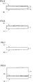
- substrate 2 having backside surface 2B allowing the ratio of peak strengths to be substantially 0 was employed as follows.
- the present inventors have found that one of causes of increase of the resistivity of a substrate 2 made of SiC having a 4H type single-crystal structure is extension of stacking faults that are specified by the existence of the peak in a wavelength of around 500 nm in the photoluminescence measurement and that are formed from defects in a processing damage layer during the steps in manufacturing semiconductor device 1, in particular, during a step involving heating.
- the ratio is substantially 0, which is the most preferable, but the ratio does not need to be always substantially 0.
- the ratio is 0.01 or smaller, a large effect is obtained.
- the ratio is 0.1 or smaller, an effect is obtained.
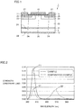
- p regions 23 of p type conductivity are formed with a space interposed therebetween.
- n + region 24 is formed at a region including the main surface of p region 23.
- a p + region 25 is formed at a location adjacent to n + region 24, a p + region 25 is formed.
- Oxide film 26 is formed to extend on n + region 24 in one p region 23, p region 23, an exposed portion of breakdown voltage holding layer 22 between the two p regions 23, the other p region 23, and n + region 24 in the other p region 23.
- Oxide film 26 can have a thickness of, for example, 40 nm.
- gate electrode 10 is formed on oxide film 26, gate electrode 10 is formed.
- the maximum value of a nitrogen atom concentration is 1 ⁇ 10 21 cm -3 or greater in a region within 10 nm from an interface between oxide film 26 and the semiconductor layer, i.e., each of n + regions 24, p + regions 25, p regions 23, and breakdown voltage holding layer 22. This achieves improved mobility particularly in a channel region below oxide film 26 (a contact portion of each p region 23 with oxide film 26 between each of n + regions 24 and breakdown voltage holding layer 22).
- main surface 2A of substrate 2 at the buffer layer 21 side preferably has an off angle of not less than 50° and not more than 65° relative to a plane orientation of ⁇ 0001 ⁇ , more preferably has an off angle of approximately 53° relative thereto.
- the off angle may have an off orientation falling within a range of ⁇ 5° or smaller relative to the ⁇ 11-20> direction.
- the off angle may have an off orientation falling within a range of ⁇ 5° or smaller relative to the ⁇ 01-10> direction.
- main surface 2A has an off angle of not less than -3° and not more than +5° relative to the ⁇ 03-38 ⁇ plane in the ⁇ 01-10> direction.
- main surface 2A has an off angle of not less than -3° and not more than +5° relative to the (0-33-8) plane in the ⁇ 01-10> direction.
- each of p regions 23 formed by epitaxial growth and impurity implantation to main surface 2A has a main surface opposite to substrate 2 and corresponding to substantially the (0-33-8) plane.
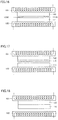
- a silicon carbide substrate preparing step S10 ( Fig. 3 ) is performed.
- substrate 2 is a silicon carbide substrate having n type conductivity and having main surface 2A corresponding to the plane with a plane orientation of (0-33-8).
- a substrate can be obtained by means of, for example, a technique of cutting an ingot (source material crystal) having a main surface corresponding to the (0001) plane, to obtain the substrate having main surface 2A exposed and corresponding to the (0-33-8) plane.
- a substrate may be employed which has n type conductivity and has a substrate resistance of 0.02 ⁇ cm, for example. Specifically, the following steps shown in Fig. 4 to Fig. 7 are performed.
- processing damage layers 2p are a layer having a strain in its crystal structure, and has a thickness of, for example, approximately 10 ⁇ m.
- processing damage layer 2p on backside surface 2B is removed.
- at least one of the following methods can be used: a method employing fused KOH etching; a method employing dry etching; a method employing thermal etching; and a method employing polishing.
- the thermal etching refers to a method for removing SiC mainly by high temperature heating.
- one of the following methods can be also used: a method of sublimating SiC; and a method of removing SiC by exposing SiC to a specific atmosphere at a high temperature.
- processing damage layer 2p on backside surface 2B is removed by means of a chemical method instead of a mechanical method or a physical method, so as not to form a new processing damage layer when removing processing damage layer 2p.
- processing damage layer 2p is removed using the mechanical method, the removal is performed under conditions allowing for mechanical damage as small as possible.
- CMP Chemical Mechanical Polishing
- the simple mechanical polishing it is preferable to use a polishing material having a particle diameter of approximately 3 ⁇ m or smaller.
- the sheet resistance of substrate 2 was increased during the steps in manufacturing semiconductor device 1, in particular, was drastically increased after the strong heat treatment. Further, as a result of performing the measurement of the sheet resistance by removing the backside surface of the substrate by 100 ⁇ m, it was found that the resistivity of this removed portion was approximately 1.3 times as large as that of the remaining portion. Namely, the substrate of the comparative example has a particularly high resistivity in the vicinity of the backside surface.
- a semiconductor device in the present embodiment has a combined substrate 2Xa instead of substrate 2 of semiconductor device 1 ( Fig. 1 ) of the foregoing first embodiment.
- Combined substrate 2Xa includes a base layer 110 made of SiC, and a substrate 120 disposed on one main surface 110A of base layer 110.
- Substrate 120 is configured the same as substrate 2 ( Fig. 7 : the first embodiment), and has a main surface 120A corresponding to main surface 2A of substrate 2, and has a backside surface 120B corresponding to the backside surface of substrate 2.
- drain electrode 12 is provided on backside surface 120B with base layer 110 interposed therebetween.
- base layer 110 and substrate 120 are made of different crystals.
- Substrate 120 has a defect density smaller than that of base layer 110.
- substrate 120 has the reduced defect densities such as the micro pipe density, the threading screw dislocation density, the threading edge dislocation density, the basal plane dislocation density, the composite dislocation density, the stacking fault density, and the point defect density.
- Such a substrate 120 allows a high-quality active layer (epitaxial growth layer) to be formed on substrate 120.
- a connecting step is performed. Specifically, by heating base layer 110 and substrate 120 stacked on each other to fall within, for example, a range of temperature equal to or greater than the sublimation temperature of SiC, base layer 110 and substrate 120 are connected to each other. Accordingly, combined substrate 2Xa ( Fig. 13 ) is obtained. Further, in the method for manufacturing the semiconductor device in the present embodiment, semiconductor device 1 is manufactured in the same manner as in the first embodiment, using this combined substrate 2Xa.
- a semiconductor device in the present embodiment has basically the same structure as that of the second or third embodiment. However, a combined substrate prepared during the step in manufacturing the semiconductor device in the fourth embodiment is different from that of the second or third embodiment.
- a combined substrate 2Xb prepared in the method for manufacturing the semiconductor device in the fourth embodiment has a plurality of substrates 120, each of which is disposed on base layer 110.
- the plurality of layers 120 are arranged in the form of a matrix on base layer 110 such that adjacent substrates 120 are in contact with each other. Accordingly, during the steps in manufacturing the semiconductor device, combined substrate 2Xb can be handled as a substrate having a large diameter and having the plurality of high-quality substrates 120. Accordingly, the process of manufacturing the semiconductor device can become efficient.
- a metal film forming step is performed as a step S112.
- the metal film is formed by, for example, depositing the metal on one main surface of base layer 110 prepared in step S110.
- This metal film includes, for example, at least one of metals forming silicide when being heated, such as nickel, molybdenum, titanium, aluminum, and tungsten.
- step S130 substrate 120 prepared in step S110 is placed on the metal film formed in step S112. In this way, a stacked substrate is obtained in which substrate 120 is provided over base substrate 110 with the metal film interposed therebetween.
- a heating step is performed.
- the stacked substrate fabricated in step S130 is heated to approximately 1000°C in an inert gas atmosphere such as argon, for example.
- an inert gas atmosphere such as argon, for example.
- the metal film a region thereof making contact with base layer 110 and a region thereof making contact with the SiC substrate
- ohmic contact layer 150 making ohmic contact with base layer 110 and substrate 120.
- combined substrate 2Xd can be readily manufactured in which base layer 110 and substrate 120 different in impurity concentration are connected to each other by ohmic contact layer 150, for example.
- step S130 referring to Fig. 26 , substrate 120 is placed on and in contact with precursor layer 161 formed on and in contact with the main surface of base layer 110, thereby fabricating a stacked substrate.
Landscapes
- Recrystallisation Techniques (AREA)
- Crystals, And After-Treatments Of Crystals (AREA)
- Electrodes Of Semiconductors (AREA)
- Insulated Gate Type Field-Effect Transistor (AREA)
Claims (7)
- Verfahren zur Herstellung einer Halbleitervorrichtung (1) mit einem Strompfad, das die folgenden Schritte umfasst:Herstellen eines Substrats (2, 120), das eine erste Oberfläche (2A, 120A) und eine der ersten Oberfläche gegenüberliegende zweite Oberfläche (2B, 120B) aufweist und das aus Siliziumkarbid mit einer 4H-Einkristallstruktur hergestellt ist, wobei im Substratherstellungsschritt auf der zweiten Oberfläche eine beschädigte Prozessschicht (2p) gebildet wird;Entfernen der beschädigten Prozessschicht auf der zweiten Oberfläche;Ausbilden einer Halbleiterschicht (21-25) auf der ersten Oberfläche, die zumindest einen Teil des Strompfades bildet und aus Siliziumkarbid gebildet ist;Erwärmen des Substrats und der Halbleiterschicht nach dem Schritt des Entfernens der beschädigten Prozessschicht, undPolieren der ersten Oberfläche vor dem Schritt des Ausbildens der Halbleiterschicht,ferner umfassend den Schritt des Ausbildens einer Basisschicht (110) aus Siliziumkarbid auf der zweiten Oberfläche (2B, 120B) nach dem Schritt des Entfernens der beschädigten Prozessschicht und vor dem Schritt des Ausbildens der Halbleiterschicht.
- Verfahren zur Herstellung der Halbleitervorrichtung nach Anspruch 1, wobei der Schritt des Erwärmens des Substrats und der Halbleiterschicht den Schritt des Ausbildens eines Isolierfilms (26) auf der Halbleiterschicht durch thermisches Oxidieren einer Oberfläche der Halbleiterschicht umfasst.
- Verfahren zur Herstellung der Halbleitervorrichtung nach Anspruch 1, wobei:
der Schritt des Herstellens des Substrats die folgenden Schritte umfasst:Herstellen eines Ingots (2Z) aus Siliziumkarbid mit einer 4H-Einkristallstruktur, undAusbilden der zweiten Oberfläche durch Schneiden des Ingots. - Verfahren zur Herstellung der Halbleitervorrichtung nach Anspruch 1, wobei der Schritt des Entfernens der beschädigten Prozessschicht den Schritt des Entfernens der beschädigten Prozessschicht durch Schmelz-KOH-Ätzen umfasst.
- Verfahren zur Herstellung der Halbleitervorrichtung nach Anspruch 1, wobei der Schritt des Entfernens der beschädigten Prozessschicht den Schritt des Entfernens der beschädigten Prozessschicht durch Trockenätzen umfasst.
- Verfahren zur Herstellung der Halbleitervorrichtung nach Anspruch 1, wobei der Schritt des Entfernens der beschädigten Prozessschicht den Schritt des Sublimierens der beschädigten Prozessschicht umfasst.
- Verfahren zum Herstellen der Halbleitervorrichtung nach Anspruch 1, wobei der Schritt des Entfernens der beschädigten Prozessschicht den Schritt des Entfernens der beschädigten Prozessschicht durch Polieren der zweiten Oberfläche (2B) des Substrats (2) umfasst.
Priority Applications (1)
| Application Number | Priority Date | Filing Date | Title |
|---|---|---|---|
| EP21162022.4A EP3869537A1 (de) | 2010-03-23 | 2010-12-20 | Halbleiterbauelement und verfahren zur herstellung davon |
Applications Claiming Priority (2)
| Application Number | Priority Date | Filing Date | Title |
|---|---|---|---|
| JP2010066197 | 2010-03-23 | ||
| PCT/JP2010/072871 WO2011118104A1 (ja) | 2010-03-23 | 2010-12-20 | 半導体装置およびその製造方法 |
Related Child Applications (2)
| Application Number | Title | Priority Date | Filing Date |
|---|---|---|---|
| EP21162022.4A Division EP3869537A1 (de) | 2010-03-23 | 2010-12-20 | Halbleiterbauelement und verfahren zur herstellung davon |
| EP21162022.4A Division-Into EP3869537A1 (de) | 2010-03-23 | 2010-12-20 | Halbleiterbauelement und verfahren zur herstellung davon |
Publications (3)
| Publication Number | Publication Date |
|---|---|
| EP2551891A1 EP2551891A1 (de) | 2013-01-30 |
| EP2551891A4 EP2551891A4 (de) | 2014-07-02 |
| EP2551891B1 true EP2551891B1 (de) | 2021-09-01 |
Family
ID=44672687
Family Applications (2)
| Application Number | Title | Priority Date | Filing Date |
|---|---|---|---|
| EP21162022.4A Withdrawn EP3869537A1 (de) | 2010-03-23 | 2010-12-20 | Halbleiterbauelement und verfahren zur herstellung davon |
| EP10848496.5A Active EP2551891B1 (de) | 2010-03-23 | 2010-12-20 | Halbleitervorrichtung und herstellungsverfahren dafür |
Family Applications Before (1)
| Application Number | Title | Priority Date | Filing Date |
|---|---|---|---|
| EP21162022.4A Withdrawn EP3869537A1 (de) | 2010-03-23 | 2010-12-20 | Halbleiterbauelement und verfahren zur herstellung davon |
Country Status (9)
| Country | Link |
|---|---|
| US (2) | US9947782B2 (de) |
| EP (2) | EP3869537A1 (de) |
| JP (2) | JP5737281B2 (de) |
| KR (1) | KR20130006442A (de) |
| CN (2) | CN105789029B (de) |
| CA (1) | CA2793969A1 (de) |
| DE (1) | DE202010018325U1 (de) |
| TW (1) | TW201140834A (de) |
| WO (1) | WO2011118104A1 (de) |
Families Citing this family (12)
| Publication number | Priority date | Publication date | Assignee | Title |
|---|---|---|---|---|
| JP6119100B2 (ja) * | 2012-02-01 | 2017-04-26 | 住友電気工業株式会社 | 炭化珪素半導体装置 |
| US11309389B2 (en) * | 2012-11-30 | 2022-04-19 | Lx Semicon Co., Ltd. | Epitaxial wafer and switch element and light-emitting element using same |
| JP6070155B2 (ja) | 2012-12-18 | 2017-02-01 | 住友電気工業株式会社 | 炭化珪素半導体装置 |
| US9631962B2 (en) * | 2014-03-18 | 2017-04-25 | Rosemount Inc. | Magnetic core configuration for magnetic flowmeters having a plurality of layers of magnetically permeable material |
| US20150364550A1 (en) * | 2014-06-16 | 2015-12-17 | Infineon Technologies Ag | Optimized layer for semiconductor |
| JP6926261B2 (ja) * | 2016-07-06 | 2021-08-25 | 株式会社東芝 | 半導体装置及びその製造方法 |
| DE102017127169B4 (de) | 2017-11-17 | 2022-01-27 | Infineon Technologies Ag | Verfahren zur herstellung eines halbleiterbauelements |
| DE102019111377B4 (de) * | 2018-05-28 | 2025-10-09 | Infineon Technologies Ag | Verfahren zum Verarbeiten eines Siliziumkarbid-Wafers |
| JP7447392B2 (ja) * | 2018-09-10 | 2024-03-12 | 株式会社レゾナック | SiC基板の評価方法及びSiCエピタキシャルウェハの製造方法 |
| JP7686989B2 (ja) * | 2021-02-09 | 2025-06-03 | 富士電機株式会社 | 炭化珪素半導体装置および炭化珪素半導体装置の製造方法 |
| JP2024080948A (ja) * | 2022-12-05 | 2024-06-17 | 株式会社デンソー | 炭化珪素基板およびそれを用いた炭化珪素半導体装置 |
| WO2025023079A1 (ja) * | 2023-07-24 | 2025-01-30 | 株式会社デンソー | 炭化珪素半導体装置の製造方法 |
Family Cites Families (18)
| Publication number | Priority date | Publication date | Assignee | Title |
|---|---|---|---|---|
| JPH0797299A (ja) | 1993-09-28 | 1995-04-11 | Nippon Steel Corp | SiC単結晶の成長方法 |
| JP3385938B2 (ja) | 1997-03-05 | 2003-03-10 | 株式会社デンソー | 炭化珪素半導体装置及びその製造方法 |
| JP4457432B2 (ja) | 1999-06-17 | 2010-04-28 | 株式会社デンソー | 種結晶とそれを用いた炭化珪素単結晶の製造方法、炭化珪素単結晶体および単結晶製造装置 |
| DE60033829T2 (de) * | 1999-09-07 | 2007-10-11 | Sixon Inc. | SiC-HALBLEITERSCHEIBE, SiC-HALBLEITERBAUELEMENT SOWIE HERSTELLUNGSVERFAHREN FÜR EINE SiC-HALBLEITERSCHEIBE |
| WO2001093339A1 (en) * | 2000-05-31 | 2001-12-06 | Matsushita Electric Industrial Co. Ltd. | Misfet |
| JP3785067B2 (ja) * | 2001-08-22 | 2006-06-14 | 株式会社東芝 | 半導体素子の製造方法 |
| US7407837B2 (en) * | 2004-01-27 | 2008-08-05 | Fuji Electric Holdings Co., Ltd. | Method of manufacturing silicon carbide semiconductor device |
| US20070290211A1 (en) * | 2004-03-26 | 2007-12-20 | The Kansai Electric Power Co., Inc. | Bipolar Semiconductor Device and Process for Producing the Same |
| JP4539140B2 (ja) | 2004-03-29 | 2010-09-08 | 住友電気工業株式会社 | 炭化珪素基板およびその製造方法 |
| US20080261401A1 (en) * | 2004-04-08 | 2008-10-23 | Ii-Vi Incorporated | Chemical-Mechanical Polishing of Sic Surfaces Using Hydrogen Peroxide or Ozonated Water Solutions in Combination with Colloidal Abrasive |
| US7314521B2 (en) | 2004-10-04 | 2008-01-01 | Cree, Inc. | Low micropipe 100 mm silicon carbide wafer |
| WO2009019837A1 (ja) * | 2007-08-07 | 2009-02-12 | Panasonic Corporation | 炭化珪素半導体素子およびその製造方法 |
| JP2009130266A (ja) | 2007-11-27 | 2009-06-11 | Toshiba Corp | 半導体基板および半導体装置、半導体装置の製造方法 |
| JP5157843B2 (ja) | 2007-12-04 | 2013-03-06 | 住友電気工業株式会社 | 炭化ケイ素半導体装置およびその製造方法 |
| JP5504597B2 (ja) | 2007-12-11 | 2014-05-28 | 住友電気工業株式会社 | 炭化ケイ素半導体装置およびその製造方法 |
| JP2009194216A (ja) | 2008-02-15 | 2009-08-27 | Hitachi Ltd | 半導体装置の製造方法 |
| JP4935741B2 (ja) | 2008-04-02 | 2012-05-23 | 三菱電機株式会社 | 炭化珪素半導体装置の製造方法 |
| JP2009256159A (ja) * | 2008-04-14 | 2009-11-05 | Incubation Alliance Inc | 結晶炭化珪素基板の製造方法 |
-
2010
- 2010-12-20 EP EP21162022.4A patent/EP3869537A1/de not_active Withdrawn
- 2010-12-20 CN CN201610129950.3A patent/CN105789029B/zh active Active
- 2010-12-20 CN CN201080065662.7A patent/CN102812537B/zh active Active
- 2010-12-20 CA CA2793969A patent/CA2793969A1/en not_active Abandoned
- 2010-12-20 EP EP10848496.5A patent/EP2551891B1/de active Active
- 2010-12-20 DE DE202010018325.1U patent/DE202010018325U1/de not_active Expired - Lifetime
- 2010-12-20 KR KR1020127023726A patent/KR20130006442A/ko not_active Withdrawn
- 2010-12-20 JP JP2012506779A patent/JP5737281B2/ja active Active
- 2010-12-20 WO PCT/JP2010/072871 patent/WO2011118104A1/ja not_active Ceased
- 2010-12-20 US US13/634,860 patent/US9947782B2/en active Active
-
2011
- 2011-01-26 TW TW100102957A patent/TW201140834A/zh unknown
-
2015
- 2015-04-17 JP JP2015084835A patent/JP6218773B2/ja active Active
-
2018
- 2018-03-12 US US15/918,652 patent/US10741683B2/en active Active
Also Published As
| Publication number | Publication date |
|---|---|
| JP2015159316A (ja) | 2015-09-03 |
| EP2551891A1 (de) | 2013-01-30 |
| EP3869537A1 (de) | 2021-08-25 |
| US20130009171A1 (en) | 2013-01-10 |
| KR20130006442A (ko) | 2013-01-16 |
| EP2551891A4 (de) | 2014-07-02 |
| CN102812537A (zh) | 2012-12-05 |
| US10741683B2 (en) | 2020-08-11 |
| CN102812537B (zh) | 2016-03-16 |
| CN105789029A (zh) | 2016-07-20 |
| US20180204942A1 (en) | 2018-07-19 |
| DE202010018325U1 (de) | 2015-08-18 |
| JP6218773B2 (ja) | 2017-10-25 |
| US9947782B2 (en) | 2018-04-17 |
| TW201140834A (en) | 2011-11-16 |
| JP5737281B2 (ja) | 2015-06-17 |
| JPWO2011118104A1 (ja) | 2013-07-04 |
| CN105789029B (zh) | 2018-08-31 |
| CA2793969A1 (en) | 2011-09-29 |
| WO2011118104A1 (ja) | 2011-09-29 |
Similar Documents
| Publication | Publication Date | Title |
|---|---|---|
| EP2551891B1 (de) | Halbleitervorrichtung und herstellungsverfahren dafür | |
| EP2490247A1 (de) | Herstellungsverfahren für ein siliciumcarbidsubstrat und siliciumcarbidsubstrat | |
| US20120056202A1 (en) | Semiconductor device | |
| US8513676B2 (en) | Semiconductor device and method for manufacturing same | |
| EP2495750A1 (de) | Herstellungsverfahren für ein siliciumcarbidsubstrat und siliciumcarbidsubstrat | |
| US20120056203A1 (en) | Semiconductor device | |
| US20110278594A1 (en) | Method for manufacturing silicon carbide substrate, method for manufacturing semiconductor device, silicon carbide substrate, and semiconductor device | |
| EP2518757A1 (de) | Siliciumcarbidsubstrat | |
| US20120126251A1 (en) | Method for manufacturing silicon carbide substrate, method for manufacturing semiconductor device, silicon carbide substrate, and semiconductor device | |
| US20110284872A1 (en) | Method for manufacturing silicon carbide substrate, method for manufacturing semiconductor device, silicon carbide substrate, and semiconductor device | |
| US20110275224A1 (en) | Method for manufacturing silicon carbide substrate | |
| US20110198027A1 (en) | Method for manufacturing silicon carbide substrate | |
| US20110272087A1 (en) | Method for manufacturing silicon carbide substrate |
Legal Events
| Date | Code | Title | Description |
|---|---|---|---|
| PUAI | Public reference made under article 153(3) epc to a published international application that has entered the european phase |
Free format text: ORIGINAL CODE: 0009012 |
|
| 17P | Request for examination filed |
Effective date: 20120920 |
|
| AK | Designated contracting states |
Kind code of ref document: A1 Designated state(s): AL AT BE BG CH CY CZ DE DK EE ES FI FR GB GR HR HU IE IS IT LI LT LU LV MC MK MT NL NO PL PT RO RS SE SI SK SM TR |
|
| DAX | Request for extension of the european patent (deleted) | ||
| A4 | Supplementary search report drawn up and despatched |
Effective date: 20140602 |
|
| RIC1 | Information provided on ipc code assigned before grant |
Ipc: H01L 29/739 20060101ALI20140526BHEP Ipc: H01L 21/02 20060101AFI20140526BHEP Ipc: H01L 21/336 20060101ALI20140526BHEP Ipc: H01L 29/12 20060101ALI20140526BHEP Ipc: H01L 29/78 20060101ALI20140526BHEP |
|
| STAA | Information on the status of an ep patent application or granted ep patent |
Free format text: STATUS: EXAMINATION IS IN PROGRESS |
|
| 17Q | First examination report despatched |
Effective date: 20181018 |
|
| GRAP | Despatch of communication of intention to grant a patent |
Free format text: ORIGINAL CODE: EPIDOSNIGR1 |
|
| STAA | Information on the status of an ep patent application or granted ep patent |
Free format text: STATUS: GRANT OF PATENT IS INTENDED |
|
| INTG | Intention to grant announced |
Effective date: 20210517 |
|
| RIN1 | Information on inventor provided before grant (corrected) |
Inventor name: MIYAZAKI, TOMIHITO Inventor name: WADA, KEIJI Inventor name: OKITA, KYOKO Inventor name: NISHIGUCHI, TARO Inventor name: SASAKI, MAKOTO Inventor name: HARADA, SHIN |
|
| GRAS | Grant fee paid |
Free format text: ORIGINAL CODE: EPIDOSNIGR3 |
|
| GRAA | (expected) grant |
Free format text: ORIGINAL CODE: 0009210 |
|
| STAA | Information on the status of an ep patent application or granted ep patent |
Free format text: STATUS: THE PATENT HAS BEEN GRANTED |
|
| AK | Designated contracting states |
Kind code of ref document: B1 Designated state(s): AL AT BE BG CH CY CZ DE DK EE ES FI FR GB GR HR HU IE IS IT LI LT LU LV MC MK MT NL NO PL PT RO RS SE SI SK SM TR |
|
| REG | Reference to a national code |
Ref country code: GB Ref legal event code: FG4D |
|
| REG | Reference to a national code |
Ref country code: CH Ref legal event code: EP Ref country code: AT Ref legal event code: REF Ref document number: 1427105 Country of ref document: AT Kind code of ref document: T Effective date: 20210915 |
|
| REG | Reference to a national code |
Ref country code: DE Ref legal event code: R096 Ref document number: 602010067532 Country of ref document: DE |
|
| REG | Reference to a national code |
Ref country code: IE Ref legal event code: FG4D |
|
| REG | Reference to a national code |
Ref country code: LT Ref legal event code: MG9D |
|
| REG | Reference to a national code |
Ref country code: NL Ref legal event code: MP Effective date: 20210901 |
|
| PG25 | Lapsed in a contracting state [announced via postgrant information from national office to epo] |
Ref country code: HR Free format text: LAPSE BECAUSE OF FAILURE TO SUBMIT A TRANSLATION OF THE DESCRIPTION OR TO PAY THE FEE WITHIN THE PRESCRIBED TIME-LIMIT Effective date: 20210901 Ref country code: SE Free format text: LAPSE BECAUSE OF FAILURE TO SUBMIT A TRANSLATION OF THE DESCRIPTION OR TO PAY THE FEE WITHIN THE PRESCRIBED TIME-LIMIT Effective date: 20210901 Ref country code: BG Free format text: LAPSE BECAUSE OF FAILURE TO SUBMIT A TRANSLATION OF THE DESCRIPTION OR TO PAY THE FEE WITHIN THE PRESCRIBED TIME-LIMIT Effective date: 20211201 Ref country code: LT Free format text: LAPSE BECAUSE OF FAILURE TO SUBMIT A TRANSLATION OF THE DESCRIPTION OR TO PAY THE FEE WITHIN THE PRESCRIBED TIME-LIMIT Effective date: 20210901 Ref country code: RS Free format text: LAPSE BECAUSE OF FAILURE TO SUBMIT A TRANSLATION OF THE DESCRIPTION OR TO PAY THE FEE WITHIN THE PRESCRIBED TIME-LIMIT Effective date: 20210901 Ref country code: NO Free format text: LAPSE BECAUSE OF FAILURE TO SUBMIT A TRANSLATION OF THE DESCRIPTION OR TO PAY THE FEE WITHIN THE PRESCRIBED TIME-LIMIT Effective date: 20211201 Ref country code: ES Free format text: LAPSE BECAUSE OF FAILURE TO SUBMIT A TRANSLATION OF THE DESCRIPTION OR TO PAY THE FEE WITHIN THE PRESCRIBED TIME-LIMIT Effective date: 20210901 Ref country code: FI Free format text: LAPSE BECAUSE OF FAILURE TO SUBMIT A TRANSLATION OF THE DESCRIPTION OR TO PAY THE FEE WITHIN THE PRESCRIBED TIME-LIMIT Effective date: 20210901 |
|
| REG | Reference to a national code |
Ref country code: AT Ref legal event code: MK05 Ref document number: 1427105 Country of ref document: AT Kind code of ref document: T Effective date: 20210901 |
|
| PG25 | Lapsed in a contracting state [announced via postgrant information from national office to epo] |
Ref country code: PL Free format text: LAPSE BECAUSE OF FAILURE TO SUBMIT A TRANSLATION OF THE DESCRIPTION OR TO PAY THE FEE WITHIN THE PRESCRIBED TIME-LIMIT Effective date: 20210901 Ref country code: LV Free format text: LAPSE BECAUSE OF FAILURE TO SUBMIT A TRANSLATION OF THE DESCRIPTION OR TO PAY THE FEE WITHIN THE PRESCRIBED TIME-LIMIT Effective date: 20210901 Ref country code: GR Free format text: LAPSE BECAUSE OF FAILURE TO SUBMIT A TRANSLATION OF THE DESCRIPTION OR TO PAY THE FEE WITHIN THE PRESCRIBED TIME-LIMIT Effective date: 20211202 |
|
| PG25 | Lapsed in a contracting state [announced via postgrant information from national office to epo] |
Ref country code: AT Free format text: LAPSE BECAUSE OF FAILURE TO SUBMIT A TRANSLATION OF THE DESCRIPTION OR TO PAY THE FEE WITHIN THE PRESCRIBED TIME-LIMIT Effective date: 20210901 |
|
| PG25 | Lapsed in a contracting state [announced via postgrant information from national office to epo] |
Ref country code: IS Free format text: LAPSE BECAUSE OF FAILURE TO SUBMIT A TRANSLATION OF THE DESCRIPTION OR TO PAY THE FEE WITHIN THE PRESCRIBED TIME-LIMIT Effective date: 20220101 Ref country code: SM Free format text: LAPSE BECAUSE OF FAILURE TO SUBMIT A TRANSLATION OF THE DESCRIPTION OR TO PAY THE FEE WITHIN THE PRESCRIBED TIME-LIMIT Effective date: 20210901 Ref country code: SK Free format text: LAPSE BECAUSE OF FAILURE TO SUBMIT A TRANSLATION OF THE DESCRIPTION OR TO PAY THE FEE WITHIN THE PRESCRIBED TIME-LIMIT Effective date: 20210901 Ref country code: RO Free format text: LAPSE BECAUSE OF FAILURE TO SUBMIT A TRANSLATION OF THE DESCRIPTION OR TO PAY THE FEE WITHIN THE PRESCRIBED TIME-LIMIT Effective date: 20210901 Ref country code: PT Free format text: LAPSE BECAUSE OF FAILURE TO SUBMIT A TRANSLATION OF THE DESCRIPTION OR TO PAY THE FEE WITHIN THE PRESCRIBED TIME-LIMIT Effective date: 20220103 Ref country code: NL Free format text: LAPSE BECAUSE OF FAILURE TO SUBMIT A TRANSLATION OF THE DESCRIPTION OR TO PAY THE FEE WITHIN THE PRESCRIBED TIME-LIMIT Effective date: 20210901 Ref country code: EE Free format text: LAPSE BECAUSE OF FAILURE TO SUBMIT A TRANSLATION OF THE DESCRIPTION OR TO PAY THE FEE WITHIN THE PRESCRIBED TIME-LIMIT Effective date: 20210901 Ref country code: CZ Free format text: LAPSE BECAUSE OF FAILURE TO SUBMIT A TRANSLATION OF THE DESCRIPTION OR TO PAY THE FEE WITHIN THE PRESCRIBED TIME-LIMIT Effective date: 20210901 Ref country code: AL Free format text: LAPSE BECAUSE OF FAILURE TO SUBMIT A TRANSLATION OF THE DESCRIPTION OR TO PAY THE FEE WITHIN THE PRESCRIBED TIME-LIMIT Effective date: 20210901 |
|
| REG | Reference to a national code |
Ref country code: DE Ref legal event code: R097 Ref document number: 602010067532 Country of ref document: DE |
|
| PLBE | No opposition filed within time limit |
Free format text: ORIGINAL CODE: 0009261 |
|
| STAA | Information on the status of an ep patent application or granted ep patent |
Free format text: STATUS: NO OPPOSITION FILED WITHIN TIME LIMIT |
|
| PG25 | Lapsed in a contracting state [announced via postgrant information from national office to epo] |
Ref country code: MC Free format text: LAPSE BECAUSE OF FAILURE TO SUBMIT A TRANSLATION OF THE DESCRIPTION OR TO PAY THE FEE WITHIN THE PRESCRIBED TIME-LIMIT Effective date: 20210901 Ref country code: IT Free format text: LAPSE BECAUSE OF FAILURE TO SUBMIT A TRANSLATION OF THE DESCRIPTION OR TO PAY THE FEE WITHIN THE PRESCRIBED TIME-LIMIT Effective date: 20210901 Ref country code: DK Free format text: LAPSE BECAUSE OF FAILURE TO SUBMIT A TRANSLATION OF THE DESCRIPTION OR TO PAY THE FEE WITHIN THE PRESCRIBED TIME-LIMIT Effective date: 20210901 |
|
| REG | Reference to a national code |
Ref country code: CH Ref legal event code: PL |
|
| 26N | No opposition filed |
Effective date: 20220602 |
|
| GBPC | Gb: european patent ceased through non-payment of renewal fee |
Effective date: 20211220 |
|
| PG25 | Lapsed in a contracting state [announced via postgrant information from national office to epo] |
Ref country code: SI Free format text: LAPSE BECAUSE OF FAILURE TO SUBMIT A TRANSLATION OF THE DESCRIPTION OR TO PAY THE FEE WITHIN THE PRESCRIBED TIME-LIMIT Effective date: 20210901 |
|
| REG | Reference to a national code |
Ref country code: BE Ref legal event code: MM Effective date: 20211231 |
|
| PG25 | Lapsed in a contracting state [announced via postgrant information from national office to epo] |
Ref country code: LU Free format text: LAPSE BECAUSE OF NON-PAYMENT OF DUE FEES Effective date: 20211220 Ref country code: IE Free format text: LAPSE BECAUSE OF NON-PAYMENT OF DUE FEES Effective date: 20211220 Ref country code: GB Free format text: LAPSE BECAUSE OF NON-PAYMENT OF DUE FEES Effective date: 20211220 |
|
| PG25 | Lapsed in a contracting state [announced via postgrant information from national office to epo] |
Ref country code: FR Free format text: LAPSE BECAUSE OF NON-PAYMENT OF DUE FEES Effective date: 20211231 Ref country code: BE Free format text: LAPSE BECAUSE OF NON-PAYMENT OF DUE FEES Effective date: 20211231 |
|
| PG25 | Lapsed in a contracting state [announced via postgrant information from national office to epo] |
Ref country code: LI Free format text: LAPSE BECAUSE OF NON-PAYMENT OF DUE FEES Effective date: 20211231 Ref country code: CH Free format text: LAPSE BECAUSE OF NON-PAYMENT OF DUE FEES Effective date: 20211231 |
|
| PG25 | Lapsed in a contracting state [announced via postgrant information from national office to epo] |
Ref country code: HU Free format text: LAPSE BECAUSE OF FAILURE TO SUBMIT A TRANSLATION OF THE DESCRIPTION OR TO PAY THE FEE WITHIN THE PRESCRIBED TIME-LIMIT; INVALID AB INITIO Effective date: 20101220 Ref country code: CY Free format text: LAPSE BECAUSE OF FAILURE TO SUBMIT A TRANSLATION OF THE DESCRIPTION OR TO PAY THE FEE WITHIN THE PRESCRIBED TIME-LIMIT Effective date: 20210901 |
|
| P01 | Opt-out of the competence of the unified patent court (upc) registered |
Effective date: 20230515 |
|
| PG25 | Lapsed in a contracting state [announced via postgrant information from national office to epo] |
Ref country code: MK Free format text: LAPSE BECAUSE OF FAILURE TO SUBMIT A TRANSLATION OF THE DESCRIPTION OR TO PAY THE FEE WITHIN THE PRESCRIBED TIME-LIMIT Effective date: 20210901 |
|
| PG25 | Lapsed in a contracting state [announced via postgrant information from national office to epo] |
Ref country code: TR Free format text: LAPSE BECAUSE OF FAILURE TO SUBMIT A TRANSLATION OF THE DESCRIPTION OR TO PAY THE FEE WITHIN THE PRESCRIBED TIME-LIMIT Effective date: 20210901 |
|
| PG25 | Lapsed in a contracting state [announced via postgrant information from national office to epo] |
Ref country code: MT Free format text: LAPSE BECAUSE OF FAILURE TO SUBMIT A TRANSLATION OF THE DESCRIPTION OR TO PAY THE FEE WITHIN THE PRESCRIBED TIME-LIMIT Effective date: 20210901 |
|
| REG | Reference to a national code |
Ref country code: DE Ref legal event code: R079 Ref document number: 602010067532 Country of ref document: DE Free format text: PREVIOUS MAIN CLASS: H01L0021020000 Ipc: H10P0095000000 |
|
| PGFP | Annual fee paid to national office [announced via postgrant information from national office to epo] |
Ref country code: DE Payment date: 20251028 Year of fee payment: 16 |