EP2553716B1 - Structures semi-conductrices iii-v et leurs procédés d'élaboration - Google Patents
Structures semi-conductrices iii-v et leurs procédés d'élaboration Download PDFInfo
- Publication number
- EP2553716B1 EP2553716B1 EP11711427.2A EP11711427A EP2553716B1 EP 2553716 B1 EP2553716 B1 EP 2553716B1 EP 11711427 A EP11711427 A EP 11711427A EP 2553716 B1 EP2553716 B1 EP 2553716B1
- Authority
- EP
- European Patent Office
- Prior art keywords
- ingan
- sublayer
- layer
- growth
- indium
- Prior art date
- Legal status (The legal status is an assumption and is not a legal conclusion. Google has not performed a legal analysis and makes no representation as to the accuracy of the status listed.)
- Active
Links
Images



Classifications
-
- H—ELECTRICITY
- H10—SEMICONDUCTOR DEVICES; ELECTRIC SOLID-STATE DEVICES NOT OTHERWISE PROVIDED FOR
- H10D—INORGANIC ELECTRIC SEMICONDUCTOR DEVICES
- H10D62/00—Semiconductor bodies, or regions thereof, of devices having potential barriers
- H10D62/80—Semiconductor bodies, or regions thereof, of devices having potential barriers characterised by the materials
- H10D62/85—Semiconductor bodies, or regions thereof, of devices having potential barriers characterised by the materials being Group III-V materials, e.g. GaAs
- H10D62/8503—Nitride Group III-V materials, e.g. AlN or GaN
-
- H—ELECTRICITY
- H10—SEMICONDUCTOR DEVICES; ELECTRIC SOLID-STATE DEVICES NOT OTHERWISE PROVIDED FOR
- H10P—GENERIC PROCESSES OR APPARATUS FOR THE MANUFACTURE OR TREATMENT OF DEVICES COVERED BY CLASS H10
- H10P14/00—Formation of materials, e.g. in the shape of layers or pillars
- H10P14/20—Formation of materials, e.g. in the shape of layers or pillars of semiconductor materials
-
- H—ELECTRICITY
- H10—SEMICONDUCTOR DEVICES; ELECTRIC SOLID-STATE DEVICES NOT OTHERWISE PROVIDED FOR
- H10P—GENERIC PROCESSES OR APPARATUS FOR THE MANUFACTURE OR TREATMENT OF DEVICES COVERED BY CLASS H10
- H10P14/00—Formation of materials, e.g. in the shape of layers or pillars
- H10P14/20—Formation of materials, e.g. in the shape of layers or pillars of semiconductor materials
- H10P14/24—Formation of materials, e.g. in the shape of layers or pillars of semiconductor materials using chemical vapour deposition [CVD]
-
- H—ELECTRICITY
- H10—SEMICONDUCTOR DEVICES; ELECTRIC SOLID-STATE DEVICES NOT OTHERWISE PROVIDED FOR
- H10P—GENERIC PROCESSES OR APPARATUS FOR THE MANUFACTURE OR TREATMENT OF DEVICES COVERED BY CLASS H10
- H10P14/00—Formation of materials, e.g. in the shape of layers or pillars
- H10P14/20—Formation of materials, e.g. in the shape of layers or pillars of semiconductor materials
- H10P14/29—Formation of materials, e.g. in the shape of layers or pillars of semiconductor materials characterised by the substrates
- H10P14/2901—Materials
-
- H—ELECTRICITY
- H10—SEMICONDUCTOR DEVICES; ELECTRIC SOLID-STATE DEVICES NOT OTHERWISE PROVIDED FOR
- H10P—GENERIC PROCESSES OR APPARATUS FOR THE MANUFACTURE OR TREATMENT OF DEVICES COVERED BY CLASS H10
- H10P14/00—Formation of materials, e.g. in the shape of layers or pillars
- H10P14/20—Formation of materials, e.g. in the shape of layers or pillars of semiconductor materials
- H10P14/32—Formation of materials, e.g. in the shape of layers or pillars of semiconductor materials characterised by intermediate layers between substrates and deposited layers
- H10P14/3202—Materials thereof
- H10P14/3214—Materials thereof being Group IIIA-VA semiconductors
-
- H—ELECTRICITY
- H10—SEMICONDUCTOR DEVICES; ELECTRIC SOLID-STATE DEVICES NOT OTHERWISE PROVIDED FOR
- H10P—GENERIC PROCESSES OR APPARATUS FOR THE MANUFACTURE OR TREATMENT OF DEVICES COVERED BY CLASS H10
- H10P14/00—Formation of materials, e.g. in the shape of layers or pillars
- H10P14/20—Formation of materials, e.g. in the shape of layers or pillars of semiconductor materials
- H10P14/32—Formation of materials, e.g. in the shape of layers or pillars of semiconductor materials characterised by intermediate layers between substrates and deposited layers
- H10P14/3202—Materials thereof
- H10P14/3214—Materials thereof being Group IIIA-VA semiconductors
- H10P14/3216—Nitrides
-
- H—ELECTRICITY
- H10—SEMICONDUCTOR DEVICES; ELECTRIC SOLID-STATE DEVICES NOT OTHERWISE PROVIDED FOR
- H10P—GENERIC PROCESSES OR APPARATUS FOR THE MANUFACTURE OR TREATMENT OF DEVICES COVERED BY CLASS H10
- H10P14/00—Formation of materials, e.g. in the shape of layers or pillars
- H10P14/20—Formation of materials, e.g. in the shape of layers or pillars of semiconductor materials
- H10P14/34—Deposited materials, e.g. layers
- H10P14/3402—Deposited materials, e.g. layers characterised by the chemical composition
-
- H—ELECTRICITY
- H10—SEMICONDUCTOR DEVICES; ELECTRIC SOLID-STATE DEVICES NOT OTHERWISE PROVIDED FOR
- H10P—GENERIC PROCESSES OR APPARATUS FOR THE MANUFACTURE OR TREATMENT OF DEVICES COVERED BY CLASS H10
- H10P14/00—Formation of materials, e.g. in the shape of layers or pillars
- H10P14/20—Formation of materials, e.g. in the shape of layers or pillars of semiconductor materials
- H10P14/34—Deposited materials, e.g. layers
- H10P14/3402—Deposited materials, e.g. layers characterised by the chemical composition
- H10P14/3414—Deposited materials, e.g. layers characterised by the chemical composition being group IIIA-VIA materials
-
- H—ELECTRICITY
- H10—SEMICONDUCTOR DEVICES; ELECTRIC SOLID-STATE DEVICES NOT OTHERWISE PROVIDED FOR
- H10P—GENERIC PROCESSES OR APPARATUS FOR THE MANUFACTURE OR TREATMENT OF DEVICES COVERED BY CLASS H10
- H10P14/00—Formation of materials, e.g. in the shape of layers or pillars
- H10P14/20—Formation of materials, e.g. in the shape of layers or pillars of semiconductor materials
- H10P14/34—Deposited materials, e.g. layers
- H10P14/3402—Deposited materials, e.g. layers characterised by the chemical composition
- H10P14/3414—Deposited materials, e.g. layers characterised by the chemical composition being group IIIA-VIA materials
- H10P14/3416—Nitrides
Definitions
- Embodiments of the present invention generally relate to III-V semiconductor structures and methods of forming III-V semiconductor structures.
- III-V semiconductor materials such as, for example, III-arsenides (e.g., Indium Gallium Arsenide(InGaAs)), III-phosphides (e.g., Indium Gallium Phosphide (InGaP)) and III-nitrides (e.g., Indium Gallium Nitride (InGaN)), may be employed in a number of electronic device structures, such as, for example, switching structures (e.g., transistors, etc.), light emitting structures (e.g., laser diodes, light emitting diodes, etc.), light receiving structures (e.g., waveguides, splitters, mixers, photodiodes, solar cells, solar subcells etc.), and/or microelectromechanical system structures (e.g., accelerometers, pressure sensors, etc).
- switching structures e.g., transistors, etc.
- light emitting structures e.g., laser diodes, light emitting diodes, etc.
- Such electronic device structures containing III-V semiconductor materials may be used in a wide variety of applications.
- such device structures are often used to produce radiation (e.g., visible light) at one or more of various wavelengths.
- the light emitted by such structures may be utilized not only for illumination applications, but may also be used in, for example, media storage and retrieval applications, printing applications, spectroscopy applications, biological agent detection applications, and image projection applications.
- InGaN a III-nitride material
- InGaN layers may be deposited heteroepitaxially on an underlying substrate, which may have a crystal lattice that does not match that of the overlying InGaN layer.
- InGaN layers may be deposited on a semiconductor substrate comprising gallium nitride (GaN).
- the GaN may have a relaxed (i.e., substantially strain free) in-plane lattice parameter of approximately 3.189 ⁇
- the InGaN layers may have a relaxed in-plane lattice parameter, depending on the corresponding percentage indium content, of approximately 3.21 ⁇ (for 7% indium, i.e., In 0.07 Ga 0.93 N), approximately 3.24 ⁇ (for 15% indium, i.e., In 0.15 Ga 0.85 N), and approximately 3.26 ⁇ (for 25% indium, i.e., In 0.25 Ga 0.75 N).
- the InGaN layer may initially grow "pseudomorphically" to the underlying substrate, such that a lattice parameter of the InGaN layer is caused (e.g., forced by atomic forces) to substantially match a lattice parameter of the underlying substrate upon which it is grown.
- the lattice mismatch between the InGaN layer and the underling substrate e.g., GaN
- the lattice mismatch between the InGaN layer and the underling substrate e.g., GaN
- the underling substrate e.g., GaN
- the strain in the InGaN layer may increase until, at a thickness commonly referred to as the "critical thickness," the InGaN layer may no longer grow in a pseudomorphic manner and may undergo strain relaxation. Strain relaxation in the InGaN layer may result in a deterioration of quality in the crystal lattice of the InGaN layer. For example, such deterioration in crystal quality in the InGaN layer may include the formation of crystalline defects (e.g., dislocations), a roughening of an InGaN layer surface, and/or the formation of regions of inhomogeneous material composition.
- crystalline defects e.g., dislocations
- the InGaN layer may incorporate an increased amount of indium.
- the percentage of indium incorporated into the InGaN layer at the growth surface thereof may increase, resulting in a non-uniform concentration of indium in the InGaN layer across the thickness thereof.
- an increase in indium concentration in the InGaN layer may promote the onset of additional strain relaxation, which may result in a further deterioration in crystal quality of the InGaN layer.
- the invention relates to methods of forming a structure comprising an indium gallium nitride (InGaN) layer according to the appended claims.
- InGaN indium gallium nitride
- III-V semiconductor means InGaN.
- indium gallium nitride and “InGaN” mean alloys of indium nitride (InN) and gallium nitride (GaN) having a composition of In x Ga 1-x N, where 0 ⁇ x ⁇ 1.
- sublayer means a layer portion of a relatively larger single layer of material.
- the term "ultimate sublayer” means the sublayer most distal from a semiconductor substrate upon which a number of sublayers are deposited.
- penultimate sublayer means the sublayer adjacent to and underlying an ultimate sublayer of a plurality of sublayers.
- critical thickness means the average total thickness of a layer of semiconductor material at which and beyond which pseudomorphic growth discontinues and the layer undergoes strain relaxation.
- growth surface means any surface of a semiconductor substrate, layer or sublayer at which additional growth of the semiconductor substrate, layer or sublayer can be carried out.
- the term “substantially” is used herein to refer to a result that is complete except for any deficiencies normally expected in the art.
- the embodiments of the invention may have applications to a wide range of III-V semiconductor materials.
- the methods and structures of the embodiments of the invention may be applied to III-nitrides, III-arsenides, III-phosphides and III-antimonides, in binary, ternary, quaternary and quinary form.
- Particular applications pertain to growing group III-nitride semiconductors containing indium, such as indium gallium nitride (InGaN). Accordingly, for conciseness and convenience only and without limitation, the following description and figures reflect common characteristics of the III-nitrides, and particularly, of InGaN.
- Experimentation in the III-nitride materials system demonstrates that InGaN layers grown heteroepitaxially to a thickness above a critical thickness, may undergo strain relaxation to relieve strain in the crystal lattice resulting from lattice mismatch.
- an increased amount of indium may be incorporated, which may result in a non-uniform concentration profile of indium across a thickness of the InGaN layers.
- an InGaN layer may include an increased indium percentage proximate to a growth surface of the layer.
- Such a non-uniform indium composition in the InGaN layer may be undesirable for at least some applications.
- strain relaxation of the InGaN layer may also result in roughening of the growth surface of the InGaN layer. Such surface roughening may be detrimental to the production of semiconductor devices using the InGaN layer. Further, experimentation has demonstrated that strain relaxation of the InGaN layer may result in an increase in a density of defects in the crystalline material. Such defects may include, for example, dislocations and regions of inhomogeneous composition (i.e., phase separated regions).
- a semiconductor structure 100 may be fabricated or otherwise provided to comprise a semiconductor substrate 102.
- Semiconductor substrate 102 may include a semiconductor material 104 that may be used as a seed layer for use in forming one or more additional sublayers of semiconductor material thereon as part of the fabrication of a III-V semiconductor layer, such as an InGaN layer, as described in further detail below.
- the layer of semiconductor material 104 may be attached to and carried by a substrate 106.
- the semiconductor material 104 may comprise a free-standing, bulk layer of semiconductor material that is not disposed on or carried by a substrate 106 or any other material.
- the layer of semiconductor material 104 may comprise an epitaxial layer of semiconductor material.
- the layer of semiconductor material 104 may comprise an epitaxial layer of III-V semiconductor material.
- the layer of semiconductor material 104 may comprise an epitaxial layer of GaN or an epitaxial layer of InGaN.
- Substrate 106 may comprise a material such as, for example, aluminum oxide (Al 2 O 3 ) (e.g ., sapphire), zinc oxide (ZnO), silicon (Si), silicon carbide (SiC), gallium arsenide (GaAs), lithium gallate (LiGaO 2 ), lithium aluminate (LiAlO 2 ), yttrium aluminum oxide (Y 3 Al 5 O 12 ), or magnesium oxide (MgO).
- Al 2 O 3 aluminum oxide
- ZnO zinc oxide
- Si silicon
- SiC silicon carbide
- GaAs gallium arsenide
- LiGaO 2 lithium gallate
- LiAlO 2 lithium aluminate
- Y 3 Al 5 O 12 yttrium aluminum oxide
- MgO magnesium oxide
- one or more intermediate layers of material may be disposed between the layer of semiconductor material 104 and the substrate 106.
- Such intermediate layers of material may be used, for example, as a seed layer for forming the layer of semiconductor material 104 thereon, or as a bonding layer for bonding the layer of semiconductor material 104 to the substrate 106, such as might be carried out when it is difficult or impossible to form the layer of semiconductor material 104 directly on the substrate 106.
- bonding of the layer of semiconductor material 104 to the substrate 106 may be desired if semiconductor material 104 is polar. In such embodiments, the bonding process may be utilized to alter the polarity of the polar semiconductor material.
- the layer of semiconductor material 104 may be relatively thin compared to the substrate 106.
- the layer of semiconductor material 104 may be epitaxially grown or otherwise formed or provided on a major surface of the substrate 106. Any of various methods known in the art may be used to reduce the density of dislocations in the layer of semiconductor material 104. Such methods include, for example, epitaxial lateral overgrowth (ELO), Pendeo epitaxy, in-situ masking techniques, etc.
- the layer of semiconductor material 104 may be deposited, for example, using a process such as metalorganic chemical vapor deposition (MOCVD), molecular beam epitaxy (MBE), or hydride vapor stage epitaxy (HVPE).
- MOCVD metalorganic chemical vapor deposition
- MBE molecular beam epitaxy
- HVPE hydride vapor stage epitaxy
- FIG. 1B illustrates semiconductor structure 110 comprising semiconductor substrate 102 and a III-V semiconductor layer 116 over the semiconductor material 104.
- III-V semiconductor layer 116 may comprise an InGaN layer.
- III-V semiconductor layer 116 may be subdivided into a number of sublayers.
- III-V semiconductor layer 116 may comprise an initial, first sublayer 112 disposed upon semiconductor substrate 102.
- First sublayer 112 may be grown to a first thickness ( D 1 ) utilizing a first set of growth conditions.
- III-V semiconductor layer 116 comprises two or more sublayers disposed one over another and grown utilizing two or more different sets of growth conditions.
- the average total thickness of the III-V semiconductor layer ( D 0 ) is equal to the sum of the thicknesses of the two or more sublayers. In other words, the sum of the thicknesses of all of the sublayers equals the average total thickness of the III-V semiconductor layer ( D 0 ).
- FIG. 1B illustrates an initial stage in the growth of III-V semiconductor layer 116, and, thus, illustrates only a portion of the III-V semiconductor layer 116 to be formed.
- the portion of the III-V semiconductor layer 116 shown in FIG. 1B comprises a first sublayer 112. Therefore, at the initial growth stage of the III-V semiconductor layer 116, the average total thickness of the III-V semiconductor layer ( D 0 ) is equal to the average thickness ( D 1 ) of the first sublayer 112.
- first sublayer 112 may be grown upon or at a growth surface 108 of semiconductor substrate 102 utilizing methods such as, for example, metalorganic chemical vapor deposition (MOCVD), molecular beam epitaxy (MBE), or hydride vapor stage epitaxy (HVPE).
- semiconductor substrate 102 may include semiconductor material 104, which may have a lattice parameter mismatch with first sublayer 112.
- at least one lattice parameter of the semiconductor material 104 in a strain-relaxed state may differ from at least one lattice parameter of the first sublayer 112 in a strain-relaxed state.
- Semiconductor material 104 comprises InGaN with a different concentration of indium compared to that of first sublayer 112. Such a mismatch in lattice parameter between semiconductor material 104 and first sublayer 112 may result in lattice strain in first sublayer 112.
- Lattice strain in first sublayer 112 may increase as the average total thickness ( D 0 ) of III-V semiconductor layer 116 increases with continued growth.
- the average total thickness ( D 1 ) of the first sublayer 112 is selected to be less than or equal to a first critical thickness ( D C1 ) of the first sublayer 112.
- the critical thickness of first sublayer 112 may be dependent on a number of parameters including, for example, the composition of first sublayer 112 (e.g., the percentage of indium in the first sublayer 112), the growth parameters utilized for the growth of first sublayer 112, and the degree of lattice mismatch between the first sublayer 112 and the underlying semiconductor layer 102 upon which first sublayer 112 is grown.
- the composition of first sublayer 112 e.g., the percentage of indium in the first sublayer 112
- the growth parameters utilized for the growth of first sublayer 112 e.g., the degree of lattice mismatch between the first sublayer 112 and the underlying semiconductor layer 102 upon which first sublayer 112 is grown.
- first sublayer 112 has an average total thickness ( D 1 ) that is less than the first critical thickness ( D C1 ) of the first sublayer 112. However, if the thickness of the first sublayer 112 were increased beyond the initial critical thickness (i.e., D 1 > D C1 ) while maintaining the initial, first set of growth conditions (which may be held constant while forming the first sublayer 112), the strain in first sublayer 112 may become sufficient to result in strain relaxation and the formation of defects in the first sublayer 112.
- FIG. 1C illustrates semiconductor structure 120 that comprises semiconductor substrate 102 and III-V semiconductor layer 116.
- III-V semiconductor layer 116 which may be, for example, an InGaN layer as discussed above, may include first sublayer 112 and a following, second sublayer 118.
- Second sublayer 118 is grown utilizing a second set of growth conditions that differs in at least one aspect from the first set of growth conditions used to form the first sublayer 112, and is selected such that the average thickness ( D 2 ) of second sublayer 118 yields an average total thickness (D 0 ) of III-V semiconductor layer 116 greater than the initial critical thickness ( D C1 ) and less than or equal to a following, second critical thickness ( D C2 ) of the second sublayer 118 (and the InGaN layer 116).
- second sublayer 118 may be grown upon growth surface 108' of first sublayer 112.
- Second sublayer 118 may be grown utilizing the growth techniques described above (e.g., MBE, MOCVD, or HVPE).
- the second sublayer 118 (D 2 ) is grown to a thickness such that the average total thickness ( D 0 ) of III-V semiconductor layer 116 increases and becomes greater than initial critical thickness ( D C1 ).
- the second set of growth conditions used to form the second sublayer 118 is selected such that the III-V semiconductor layer 116 may be substantially prevented from strain relaxing as the average total thickness of ( D 0 ) III-V semiconductor 116 increases beyond the first critical thickness ( D C1 ).
- Lattice strain in second sublayer 118 may increase further as the average total thickness ( D 0 ) of III-V semiconductor layer 116 increases with continued growth, utilizing the second set of growth conditions.
- the thickness ( D 2 ) of second sublayer 118 is selected such that the average total thickness ( D 0 ) of III-V semiconductor layer 116 is less than or equal to a following, second critical thickness ( D C2 ) of the second sublayer 118 (and the III-V semiconductor layer 116).
- III-V semiconductor layer 116 has an average total thickness ( D 0 ) that is greater than the initial, first critical thickness ( D C1 ) and less than the following, second critical thickness ( D C2 ). However, if the thickness of second sublayer 118 were increased such that the average total thickness ( D 0 ) of III-V semiconductor layer 116 met or exceeded the second critical thickness while maintaining the second set of growth conditions, the lattice strain in the III-V semiconductor layer 116 would become sufficient to result in strain relaxation of the III-V semiconductor layer 116 and the formation of associated defects therein.
- Second sublayer 118 is grown utilizing a second set of growth conditions selected such that a net rate at which the group III element is incorporated into the second sublayer 118 as the second sublayer 118 is formed is substantially equal to a net rate at which the group III element is incorporated into the first sublayer 112 as the first sublayer 112 is formed using the first set of growth conditions. Therefore, embodiments of the invention comprise methods to achieve a III-V semiconductor layer comprising a substantially uniform composition.
- the group III element comprises In and Ga and embodiments of the invention provide a III-V semiconductor layer having an at least substantially constant concentration of the group III element across a thickness of the III-V semiconductor layer, and provide a III-V semiconductor layer that is substantially free of strain relaxation and defects associated with such strain relaxation.
- the net rate at which the group III element is incorporated into a sublayer of a III-V semiconductor layer at a growth surface may be dependent on a number of factors including, for example, the incoming flux of the group III element to the growth surface, and the desorption flux of the group III element from the growth surface. Therefore, embodiments of the invention may include the regulation (e.g., selective control) of the incoming flux of the group III element to the growth surface, and/or the regulation (e.g., selective control) of the desorption flux of the group III element from the growth surface in order to maintain the net rate at which the group III element is incorporated into the III-V semiconductor layer at a growth surface as the average total thickness ( D 0 ) of III-V semiconductor layer 116 increases.
- selecting the second set of growth conditions may comprises reducing an incoming flux of the group III element to growth surface 108' during formation of the second sublayer 118, relative to an incoming flux of the group III element to growth surface 108 during formation of the first sublayer 112.
- reducing the incoming flux of the group III element to the growth surface may affect the number of the group III elemental species available for interaction.
- the rate at which the group III element is incorporated into the growing III-V semiconductor layer 116 may be maintained at least substantially constant as the average total thickness ( D 0 ) of the III-V semiconductor layer increases.
- Reducing the incoming flux of the group III element to growth surface 108' may further comprise, for example, one or more of reducing a partial pressure of a group III element precursor within a reactor in which the III-V semiconductor layer 116 is formed, reducing a reactor pressure within the reactor, reducing the group III element precursor flow rate through the reactor, reducing a ratio of the group III element precursor to an alkyl within the reactor, increasing a group-V precursor flow rate through the reactor, and increasing an inert gas flow rate through the reactor.
- Such methods for reducing an incoming flux of the group III element are known in the field of physical chemistry, and further details regarding such methods may be found in a number of reference publications including, for example, the publication of R. I.
- the following non-limiting example embodiments of the invention describe methods for maintaining a substantially constant rate of incorporation of the group III element into the III-V semiconductor layer at the growth surface thereof.
- the following description and figures pertain to a III-V semiconductor layer comprising InGaN and a group III-element comprising indium.
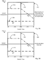
- FIG. 3A illustrates a non-limiting example embodiment of some methods of the invention, which may be used for maintaining the rate of incorporation of the group III element indium into the growth surface of III-V semiconductor layer 116 by reducing the incoming flux of the indium into the growth surface.
- FIG. 3A includes a graph 300, which illustrates the relationship between growth time, InGaN composition and the incoming flux of indium to growth surface of the III-V semiconductor layer 116.
- Line 302 represents the variation in the incoming indium flux to the growth surface as a function of growth time
- line 304 represents the composition of the InGaN layer 116 at the growth surface as a function of growth time.
- region 306 of graph 300 illustrates the growth period for the formation of the first sublayer 112 (e.g., initial InGaN sublayer) utilizing a first set of growth conditions.
- the incoming flux of indium to the growth surface may be constant over the period of growth used to form the first sublayer 112, and the composition at the growth surface of the first sublayer 112 may also be substantially constant during the growth of the first sublayer 112 such that the composition is at least substantially constant across a thickness of the first sublayer 112.
- Region 308 of graph 300 illustrates the growth period for the formation of the second sublayer 118 (e.g., following InGaN sublayer) utilizing a second set of growth conditions differing from the first set of growth conditions used to form the first sublayer 112.
- the incoming flux of indium to growth surface 108' may be reduced at a desired reduction rate after the average total thickness of InGaN layer 116 reaches the initial critical thickness ( D C1 ) at a time represented by line 310.
- D C1 initial critical thickness
- the InGaN composition of the InGaN layer may remain substantially constant, as represented by line 304.
- second sublayer 118 continues as the incoming flux of indium to growth surface 108' of the InGaN layer decreases, at most until the InGaN layer thickness equals the following critical thickness ( D C2 ) at a time represented by line 312, at which time the growth may be terminated.
- selecting the second set of growth conditions may comprise reducing an indium precursor flow rate to reduce the incoming flux of indium to the growth surface of the InGaN layer.
- the flow of indium precursor to the growth surface of InGaN layer 116 may affect the incoming flux of indium species available for interaction on the growth surface of the InGaN layer. Therefore, by reducing the indium precursor flow rate, a corresponding reduction of incoming flux of indium species to the growth surface of InGaN layer 116 may be achieved, and the rate at which indium is incorporated into the InGaN layer 116 may be maintained at least substantially constant.
- selecting a reduced indium precursor flow rate may comprise reducing an indium flow rate at a reduction rate of approximately 5 cc per minute or less, at a reduction rate of approximately 3 cc per minute or less, or even at a reduction rate of approximately than 1 cc per minute or less.
- FIG. 3B illustrates graph 314, which shows a relationship between growth time, InGaN composition, and the flow rate of the indium precursor.
- Line 316 represents the precursor flow rate as a function of growth time
- line 318 represents the composition of the InGaN layer 116 as a function of growth time of the InGaN layer 116.
- region 320 of graph 314 illustrates a growth period used to form first sublayer 112 (e.g., the initial InGaN sublayer) utilizing a first set of growth conditions.
- the indium precursor flow rate 316 is constant over the period of growth 320 for forming first sublayer 112, and the InGaN composition is also substantially constant across a thickness of first sublayer 112.
- Region 322 of graph 314 illustrates a growth period to form second sublayer 118 (e.g., following InGaN sublayer).
- the indium precursor flow rate 316 may be reduced at a selected reduction rate after the thickness of first sublayer 112 reaches the initial critical thickness ( D C1 ) at a time represented by line 324.
- the InGaN composition of the InGaN layer may remain at least substantially constant, as represented by line 316.
- the growth of the second sublayer 118 may continue as the indium precursor flow rate decreases at most until the InGaN layer thickness reaches the second critical thickness ( D C2 ) at a time represented by line 326, at which point the growth may be terminated.
- the indium precursor for the formation of InGaN layer 116 may comprise, for example, trimethylindium (TMI) and/or triethylindium (TEI).
- TMI trimethylindium
- TEI triethylindium
- the flow rate of the indium precursor for initial growth conditions may comprise, for example, a flow rate in a range extending from about 60 to about 100 cc per min. More particularly, the flow rate of the indium precursor during the second set of growth conditions may comprise, for example, a flow rate range extending from about 40 to about 80 cc per min.
- the reduction rate of the precursor flow rate during the second set of growth conditions may comprise, for example, a reduction rate in a range extending from about 0.5 to about 10 cc per minute, per minute.
- selecting the second set of growth conditions further comprises increasing a desorption flux of indium from the growth surface of the InGaN layer 116.
- increasing the desorption flux of indium from the growth surface may prevent the InGaN layer from incorporating more indium as the average total thickness of the InGaN layer increases. Therefore, by increasing the desorption flux of indium from the growth surface 108', the net rate of indium incorporation into the growing surface of the InGaN layer 116 may be maintained at least substantially constant as the average total thickness of the InGaN layer 116 increases.
- Increasing the desorption flux of indium from the growth surface 108' may further comprise, for example, one or more of decreasing a reactor growth pressure, decreasing a diffusion boundary layer thickness, and increasing a substrate rotation speed (e.g., when utilizing a rotating disc type reactor (RDR)).
- RDR rotating disc type reactor
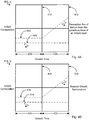
- FIG. 4A illustrates a non-limiting example embodiment of some methods outside of the invention for maintaining the net rate of incorporation of indium into InGaN layer 116 at least substantially constant by increasing the desorption flux of indium from growth surface 108'.
- FIG. 4A comprises a graph 400, which illustrates a relationship between growth time, the InGaN composition, and the desorption flux of indium from growth surface 108'.
- Line 402 represents the indium desorption flux from the growth surface as a function of growth time
- line 404 represents the composition of the InGaN layer as a function of growth time.
- region 406 of graph 400 illustrates a growth period used to form the first sublayer 112 (e.g., the initial InGaN sublayer) utilizing a first set of growth conditions.
- the desorption flux of indium from the growth surface may be constant during the period of growth used to form the first sublayer 112, and the InGaN composition may also be constant across a thickness of the first sublayer 112.
- Region 408 of graph 400 illustrates the growth time used to form the second sublayer 118 (e.g., the following InGaN sublayer) utilizing a different, second set of growth conditions.
- the desorption flux of indium from a growth surface of the InGaN layer 116 increases at a selected incrementation rate after the average total thickness ( D 0 ) of InGaN layer 116 reaches the first critical thickness ( D C1 ) at a time represented by line 410.
- the InGaN composition of the InGaN layer may remain at least substantially constant, as shown by line 404.
- the growth of the second sublayer 118 may continue as the desorption flux of indium from the growth surface of the InGaN layer increases at most until the average total InGaN layer thickness ( D 0 ) equals the second critical thickness ( D C2 ) at a time represented by line 412, at which time the growth may be terminated.
- selecting the second set of growth conditions may comprise increasing the substrate growth temperature to increase the desorption flux of indium from the growth surface of the InGaN layer 116.
- increasing the substrate growth temperature may increase the desorption flux of indium from the growth surface of the InGaN layer 116. Therefore, by increasing the substrate growth temperature, a corresponding increase in the desorption flux of indium from the growth surface 108' may be achieved, and the rate of indium incorporation in the growing InGaN layer 116 may be maintained at least substantially constant as the thickness of the InGaN layer 116 increases.
- selecting the second set of growth conditions such that the substrate growth temperature increases at a desired rate further comprises increasing the substrate growth temperature at an incrementation rate of approximately 0.5°C per minute or less, by an incrementation rate of approximately 2°C per minute or less, or even by an incrementation rate of approximately 10°C per minute or less.
- FIG. 4B illustrates graph 414 showing a relationship between growth time, InGaN composition and the substrate growth temperature.
- Line 416 represents the substrate growth temperature as a function of growth time
- line 418 represents the composition of the InGaN layer as a function of growth time.
- region 420 of graph 400 illustrates the growth period for the growth of first sublayer 112 utilizing the first set of growth conditions.
- the substrate growth temperature 416 is constant over period 420 of growth used to form the first sublayer 112, and the InGaN composition is also constant over the growth of first sublayer 112 utilizing the first set of growth conditions.
- Region 422 of graph 400 illustrates the growth period for the growth of second sublayer 118 utilizing the different, second set of growth conditions.
- the substrate growth temperature 416 increases at a selected incrementation rate after the thickness of the first sublayer 112 reaches the initial critical thickness ( D C1 ) at a time represented by line 424.
- the concentration of indium within the InGaN layer 116 may remain at least substantially constant, as shown by line 418.
- the growth of second sublayer 118 continues as the substrate temperature increases at most until the InGaN layer thickness ( D 0 ) reaches the second critical thickness ( D C2 ) at a time represented by line 426, at which point the growth may be terminated.
- the substrate growth temperature during the first set of growth conditions may comprise, for example, a growth temperature of from about 750 to about 850°C.
- the substrate growth temperature during the second set of growth conditions may comprise, for example, a reactor growth temperature of from about 800 to about 900°C.
- the incrementation rate of the reactor growth temperature during the second set of growth conditions may comprise, for example, an incrementation rate of between about 0.5 and about 10°C per minute, per minute.
- the III-V semiconductor layer 116 (i.e., a layer of InGaN) may be grown comprising an initial, first sublayer, a following, second sublayer, and one or more additional sublayers grown over the second sublayer.
- the one or more additional sublayers may be grown utilizing one or more additional growth conditions selected such that the composition of the III-V semiconductor layer 116 (i.e. an InGaN layer) is at least substantially constant across the III-V semiconductor layer 116, and such that the III-V semiconductor layer 116 is substantially free of strain relaxation.
- embodiments of the invention for growing a III-V semiconductor layer may comprise growing two or more sublayers stacked one over another utilizing two or more different sets of growth conditions, wherein the average total thickness of the III-V semiconductor layer may equal the sum of the thicknesses of the two or more sublayers.
- FIG. 2A illustrates semiconductor structure 200, which includes semiconductor structure 120 of FIG. 1C and an additional sublayer.
- the additional sublayer may comprise a penultimate sublayer 202.
- Penultimate sublayer 202 may have a thickness ( D PS ) such that the average total thickness ( D 0 ) of the III-V semiconductor layer is greater than the critical thickness of an adjacent underlying sublayer (e.g., sublayer 118 and/or sublayer 112).
- the adjacent underlying sublayer comprises second sublayer 118
- the penultimate sublayer thickness ( D PS ) yields an average total thickness ( D 0 ) of III-V semiconductor layer 116 that is greater than the second sublayer critical thickness ( D C2 )
- penultimate sublayer 202 may have a thickness (D PS ) such that the average total thickness ( D 0 ) of the III-V semiconductor layer is less than or equal to penultimate sublayer critical thickness ( D CPS ).
- FIG. 2B illustrates semiconductor structure 210, which includes semiconductor structure 200 of FIG. 2A and an ultimate sublayer 212 grown over the penultimate sublayer 202.
- Ultimate sublayer 212 may have a thickness ( D US ) such that the average total thickness ( D 0 ) of the III-V semiconductor layer is greater than the critical thickness of the adjacent, underlying penultimate sublayer 202 (i.e., such that D 0 > D CPS ) .
- ultimate sublayer 202 may have a thickness ( D US ) such that the average total thickness ( D 0 ) of the III-V semiconductor layer 116 is less than or equal to ultimate sublayer critical thickness ( D CUS ).
- III-V semiconductor layer 116 comprising four sublayers. It should be appreciated, however, that III-V semiconductor layer 116 may include two or more sublayers including for example, penultimate sublayer 202 and ultimate sublayer 212.
- growing the two or more sublayers may utilize two or more different sets of growth conditions, such that a rate of incorporation of a group III element (e.g., indium) into a growth surface of a sublayer being grown is substantially equal to a rate at which the group III element has been incorporated into a growth surface of an adjacent, underlying sublayer, such that the concentration of the group III element in the III-V semiconductor layer (i.e., InGaN) is substantially constant across a thickness of the III-V semiconductor layer.
- a group III element e.g., indium
- concentration of the group III element in the III-V semiconductor layer i.e., InGaN
- the methods for selecting the two or more different sets of growth conditions such that a rate of incorporation of a group III element (i.e. indium) into a growth surface of sublayer being grown is substantially equal to a rate at which the group III element has been previously incorporated into a growth surface of an adjacent, underling sublayer, such that the composition of the III-V semiconductor layer is substantially constant, have been described herein and may include at least one of reducing the incoming flux of the group III element into the growth surface, and increasing the desorption flux of the group III element from the growth surface, as discussed herein.
- a group III element i.e. indium
- Additional sublayers of the III-V semiconductor layer may be grown to further increase the thickness of the layer while substantially maintaining a uniform composition through an entire thickness of the III-V semiconductor layer.
- utilizing the embodiments of the invention to grow additional sublayers may enable the formation of thicker III-V semiconductor layers (e.g., InGaN layers) free of strain relaxation and associated defects, relative to at least some previously known methods.
- Embodiments of methods and structures of the present invention may be used for epitaxially growing indium gallium nitride layers.
- the methods and structures allow for the growth of InGaN semiconductor layers with substantially uniform indium concentrations, free of strain relaxation and the associated defects.
- FIGS. 5A and 5B illustrate indium gallium nitride layers grown by previously known methods different from those of the current invention.
- FIG. 5A illustrates an atomic force microscopy scan (AFM) of the growth surface 500 of an InGaN layer.
- the InGaN layer is not grown utilizing embodiments of the invention, but rather using a single set of growth conditions held constant during the entire time period over which the InGaN layer is grown.
- the InGaN growth surface 500 produced using a single set of growth conditions includes a relatively rough surface, which includes a plurality of surface pits 502. As described herein, the rough surface may be detrimental to the formation of devices using such an InGaN layer.
- FIG. 5B illustrates data produced by Ruther backscattering spectrometry (RBS), which illustrates the composition of the InGaN layer.
- RBS Ruther backscattering spectrometry
- peak 504 represents the composition of the layer of InGaN, and it is clear that the composition of the layer changes from point 506 to point 508, which indicates an increase in the concentration of indium in the layer, which may be due to strain relaxation and a subsequent increase in indium incorporation associated with such strain relaxation.
- FIGS. 5C and 5D illustrate indium gallium nitride layers grown using embodiments of the invention.
- the structure may be formed as described below with reference to FIGS. 1A-1C .
- Substrate 106 may comprise sapphire, and semiconductor layer 104 may comprise GaN grown utilizing MOCVD methods.
- the initial, first InGaN sublayer 112 may be grown using MOCVD at a temperature between about 750 and about 850°C at a reactor pressure of between about 700 and about 800 Torr utilizing an indium precursor trimethlyindium (TMI) as a source of indium.
- TMI trimethlyindium
- the TMI flow rate may be between about 70 and about 90 cc per minute with a TMI bubbler temperature of about 20°C.
- second InGaN sublayer 118 may also be grown using MOCVD at a temperature between about 750 and about 850°C at a reactor pressure between about 700 and about 800 Torr utilizing the indium precursor TMI as the source of the indium.
- the TMI flow rate may be reduced to between about 50 and about 70 cc per minute with a TMI bubbler temperature of about 20°C.
- the reduction rate in the TMI flow rate may be between about 0.5 and about 1 cc per minute.
- the InGaN layer 116 produced may have an indium concentration greater than approximately 5 % and a thickness greater than approximately 200 nm. In some embodiments, the InGaN layer produced may have an indium composition greater than approximately 8 % and a thickness greater than approximately 150 nm.
- FIG. 5D illustrates data produced by RBS from an InGaN layer grown utilizing the embodiments of the invention.
- peak 512 represents the composition of the layer of InGaN, and it is clear that the composition of the layer remains substantially unchanged from point 514 to point 516, which indicates a uniform indium concentration. Therefore the InGaN layers produced utilizing the embodiments of the invention may be relatively more suitable for device formation relative to InGaN layers formed by at least some previously known methods.
Claims (6)
- Procédé d'élaboration d'une structure comprenant une couche de nitrure de gallium-indium (InGaN), le procédé comprenant :la croissance d'une couche d'InGaN (116), comprenant :la croissance d'une première sous-couche d'InGaN (112) en utilisant un premier ensemble de conditions de croissance, etla croissance d'au moins une seconde sous-couche d'InGaN (118) sur la première sous-couche d'InGaN (112) en utilisant un second ensemble de conditions de croissance différent du premier ensemble de conditions de croissance, la première sous-couche d'InGaN (112) et l'au moins une seconde sous-couche d'InGaN (118) formant la couche d'InGaN (116),l'élaboration de la couche d'InGaN (116) de façon qu'elle ait une épaisseur totale moyenne (D0) supérieure à une épaisseur critique (DC1) de la première sous-couche d'InGaN (112) et inférieure à une épaisseur critique (Dc2) de la seconde sous-couche d'InGaN (118), dans lequel l'épaisseur critique de chaque sous-couche d'InGaN est l'épaisseur totale moyenne de ladite sous-couche à laquelle et au-delà de laquelle la croissance pseudomorphe s'arrête et ladite sous-couche subit une relaxation de contraintes, etla sélection du premier ensemble de conditions de croissance et du second ensemble de conditions de croissance de telle façon qu'un taux net d'incorporation d'indium dans une surface de croissance de la première sous-couche d'InGaN (112) soit au moins sensiblement égal à un taux net d'incorporation d'indium dans une surface de croissance de l'au moins une seconde sous-couche d'InGaN (118) de telle façon qu'une composition de la couche d'InGaN (116) reste constante à travers toute l'épaisseur totale moyenne de la couche d'InGaN,dans lequel la sélection du premier ensemble de conditions de croissance et du second ensemble de conditions de croissance comprend en outre la réduction d'un flux entrant d'indium dans la surface de croissance de l'au moins une seconde sous-couche d'InGaN (118) par rapport à un flux entrant d'indium dans la surface de croissance de la première sous-couche d'InGaN (112), ceci comprenant au moins une option parmi la diminution d'une pression partielle d'un précurseur d'indium, la réduction d'une pression de réacteur, la réduction d'un débit de précurseur, la réduction d'un ratio du précurseur d'indium par rapport à un alkyle, l'augmentation d'un débit de précurseur d'azote et l'augmentation d'un débit de gaz inerte.
- Procédé selon la revendication 1, comprenant en outre la sélection du premier ensemble de conditions de croissance et du second ensemble de conditions de croissance de telle façon que la couche d'InGaN (116) soit exempte de relaxation de contraintes.
- Procédé selon l'une quelconque des revendications précédentes, dans lequel la première étape de l'élaboration de la couche d'InGaN de façon qu'elle ait une épaisseur totale moyenne supérieure à une épaisseur critique de la première sous-couche d'InGaN et inférieure à une épaisseur critique de la seconde sous-couche d'InGaN comprend la croissance de la première sous-couche d'InGaN jusqu'à une première épaisseur inférieure ou égale à une épaisseur critique de la première sous-couche d'InGaN et la croissance de l'au moins une seconde sous-couche d'InGaN jusqu'à une épaisseur inférieure ou égale à une épaisseur critique de la seconde sous-couche d'InGaN.
- Procédé selon l'une quelconque des revendications précédentes, comprenant en outre :la croissance d'au moins une sous-couche d'InGaN supplémentaire (202, 212) sur la seconde sous-couche d'InGaN (118) en utilisant au moins un ensemble supplémentaire de conditions de croissance, etla sélection de l'au moins un ensemble supplémentaire de conditions de croissance de telle façon que la concentration d'indium dans la couche d'InGaN (116) reste sensiblement constante à travers toute l'épaisseur moyenne de la couche d'InGaN.
- Procédé selon l'une quelconque des revendications précédentes, dans lequel la sélection du second ensemble différent de conditions de croissance comprend en outre la diminution d'un débit d'un précurseur d'indium de 5 sccm par minute ou moins pendant la croissance de la seconde sous-couche d'InGaN (118) .
- Procédé d'élaboration d'une structure comprenant une couche de nitrure de gallium-indium (InGaN), le procédé comprenant :la croissance d'une couche d'InGaN (116), comprenant :la croissance d'une première sous-couche d'InGaN (112) en utilisant un premier ensemble de conditions de croissance, etla croissance d'au moins une seconde sous-couche d'InGaN (118) sur la première sous-couche d'InGaN (112) en utilisant un second ensemble de conditions de croissance différent du premier ensemble de conditions de croissance, la première sous-couche d'InGaN (112) et l'au moins une seconde sous-couche d'InGaN (118) formant la couche d'InGaN (116),l'élaboration de la couche d'InGaN (116) de façon qu'elle ait une épaisseur totale moyenne (D0) supérieure à une épaisseur critique (DC1) de la première sous-couche d'InGaN (112) et inférieure à une épaisseur critique (Dc2) de la seconde sous-couche d'InGaN (118), dans lequel l'épaisseur critique de chaque sous-couche d'InGaN est l'épaisseur totale moyenne de ladite sous-couche à laquelle et au-delà de laquelle la croissance pseudomorphe s'arrête et ladite sous-couche subit une relaxation de contraintes, etla sélection du premier ensemble de conditions de croissance et du second ensemble de conditions de croissance de telle façon qu'un taux net d'incorporation d'indium dans une surface de croissance de la première sous-couche d'InGaN (112) soit au moins sensiblement égal à un taux net d'incorporation d'indium dans une surface de croissance de l'au moins une seconde sous-couche d'InGaN (118) de telle façon qu'une composition de la couche d'InGaN (116) reste constante à travers toute l'épaisseur totale moyenne de la couche d'InGaN,dans lequel la sélection du premier ensemble de conditions de croissance et du second ensemble de conditions de croissance comprend en outre l'augmentation d'un flux de désorption d'indium depuis la surface de croissance de l'au moins une seconde sous-couche d'InGaN (118) par rapport à un flux de désorption d'indium à partir de la surface de croissance de la première sous-couche d'InGaN (112), ceci comprenant au moins une option parmi la diminution d'une pression de croissance de réacteur, la diminution d'une épaisseur de couche limite de diffusion et l'augmentation d'une vitesse de rotation du substrat.
Applications Claiming Priority (2)
| Application Number | Priority Date | Filing Date | Title |
|---|---|---|---|
| US31869310P | 2010-03-29 | 2010-03-29 | |
| PCT/US2011/029589 WO2011123303A1 (fr) | 2010-03-29 | 2011-03-23 | Structures semi-conductrices iii-v et leurs procédés d'élaboration |
Publications (2)
| Publication Number | Publication Date |
|---|---|
| EP2553716A1 EP2553716A1 (fr) | 2013-02-06 |
| EP2553716B1 true EP2553716B1 (fr) | 2018-10-17 |
Family
ID=43877231
Family Applications (1)
| Application Number | Title | Priority Date | Filing Date |
|---|---|---|---|
| EP11711427.2A Active EP2553716B1 (fr) | 2010-03-29 | 2011-03-23 | Structures semi-conductrices iii-v et leurs procédés d'élaboration |
Country Status (8)
| Country | Link |
|---|---|
| US (2) | US8377802B2 (fr) |
| EP (1) | EP2553716B1 (fr) |
| JP (1) | JP6074359B2 (fr) |
| KR (2) | KR101892610B1 (fr) |
| CN (1) | CN102822944B (fr) |
| SG (1) | SG182781A1 (fr) |
| TW (1) | TWI442455B (fr) |
| WO (1) | WO2011123303A1 (fr) |
Families Citing this family (11)
| Publication number | Priority date | Publication date | Assignee | Title |
|---|---|---|---|---|
| TWI442455B (zh) | 2010-03-29 | 2014-06-21 | S O I 矽科技絕緣體工業公司 | Iii-v族半導體結構及其形成方法 |
| WO2012064748A1 (fr) * | 2010-11-08 | 2012-05-18 | Georgia Tech Research Corporation | Systèmes et procédés de formation d'un alliage semi-conducteur à base d'un nitrure du groupe iii sans séparation de phase |
| FR2968678B1 (fr) | 2010-12-08 | 2015-11-20 | Soitec Silicon On Insulator | Procédés pour former des matériaux a base de nitrure du groupe iii et structures formées par ces procédés |
| US9023721B2 (en) | 2010-11-23 | 2015-05-05 | Soitec | Methods of forming bulk III-nitride materials on metal-nitride growth template layers, and structures formed by such methods |
| FR2968830B1 (fr) | 2010-12-08 | 2014-03-21 | Soitec Silicon On Insulator | Couches matricielles ameliorees pour le depot heteroepitaxial de materiaux semiconducteurs de nitrure iii en utilisant des procedes hvpe |
| US9076927B2 (en) * | 2012-01-13 | 2015-07-07 | The Regents Of The University Of California | (In,Ga,Al)N optoelectronic devices grown on relaxed (In,Ga,Al)N-on-GaN base layers |
| EP2862198A1 (fr) * | 2012-06-15 | 2015-04-22 | Oerlikon Advanced Technologies AG | Procédé de dépôt d'un film semi-conducteur en nitrure de groupe iii |
| CN106796965B (zh) | 2014-06-26 | 2019-07-23 | 索泰克公司 | 半导体结构及其制造方法 |
| CN109841500B (zh) * | 2018-12-19 | 2021-02-26 | 华南师范大学 | 一种InGaN外延层及其制造方法 |
| WO2020124419A1 (fr) | 2018-12-19 | 2020-06-25 | 华南师范大学 | Couche de épitaxiale d'ingan et son procédé de fabrication |
| FR3091622B1 (fr) * | 2019-01-09 | 2021-09-17 | Soitec Silicon On Insulator | Structure semi-conductrice optoélectronique comprenant une couche d’injection de type p à base d’InGaN |
Family Cites Families (12)
| Publication number | Priority date | Publication date | Assignee | Title |
|---|---|---|---|---|
| US6958093B2 (en) * | 1994-01-27 | 2005-10-25 | Cree, Inc. | Free-standing (Al, Ga, In)N and parting method for forming same |
| US6440823B1 (en) | 1994-01-27 | 2002-08-27 | Advanced Technology Materials, Inc. | Low defect density (Ga, Al, In)N and HVPE process for making same |
| JP3869641B2 (ja) * | 2000-01-31 | 2007-01-17 | 富士通株式会社 | 半導体装置及び半導体レーザ装置 |
| JP3692407B2 (ja) * | 2003-08-28 | 2005-09-07 | 国立大学法人 東京大学 | 半導体量子ドット素子の製造方法 |
| KR100895654B1 (ko) * | 2004-08-31 | 2009-05-07 | 혼다 기켄 고교 가부시키가이샤 | 질화물 반도체 결정의 성장 |
| JP2006080278A (ja) * | 2004-09-09 | 2006-03-23 | Toshiba Ceramics Co Ltd | 歪みシリコンウエハおよびその製造方法 |
| FR2895419B1 (fr) * | 2005-12-27 | 2008-02-22 | Commissariat Energie Atomique | Procede de realisation simplifiee d'une structure epitaxiee |
| US7534638B2 (en) * | 2006-12-22 | 2009-05-19 | Philips Lumiled Lighting Co., Llc | III-nitride light emitting devices grown on templates to reduce strain |
| US7951693B2 (en) * | 2006-12-22 | 2011-05-31 | Philips Lumileds Lighting Company, Llc | III-nitride light emitting devices grown on templates to reduce strain |
| WO2008094464A2 (fr) * | 2007-01-26 | 2008-08-07 | Crystal Is, Inc. | Couches épitaxiales épaisses de nitrures pseudomorphes |
| JP4539752B2 (ja) | 2008-04-09 | 2010-09-08 | 住友電気工業株式会社 | 量子井戸構造の形成方法および半導体発光素子の製造方法 |
| TWI442455B (zh) | 2010-03-29 | 2014-06-21 | S O I 矽科技絕緣體工業公司 | Iii-v族半導體結構及其形成方法 |
-
2010
- 2010-12-27 TW TW99146168A patent/TWI442455B/zh active
-
2011
- 2011-03-23 KR KR1020187012709A patent/KR101892610B1/ko active Active
- 2011-03-23 KR KR1020127025500A patent/KR20130064725A/ko not_active Ceased
- 2011-03-23 EP EP11711427.2A patent/EP2553716B1/fr active Active
- 2011-03-23 SG SG2012056081A patent/SG182781A1/en unknown
- 2011-03-23 WO PCT/US2011/029589 patent/WO2011123303A1/fr not_active Ceased
- 2011-03-23 JP JP2013502650A patent/JP6074359B2/ja active Active
- 2011-03-23 US US13/069,900 patent/US8377802B2/en active Active
- 2011-03-23 CN CN201180015070.9A patent/CN102822944B/zh active Active
-
2013
- 2013-01-10 US US13/738,406 patent/US9012919B2/en active Active
Non-Patent Citations (1)
| Title |
|---|
| None * |
Also Published As
| Publication number | Publication date |
|---|---|
| KR20180050437A (ko) | 2018-05-14 |
| KR101892610B1 (ko) | 2018-08-28 |
| CN102822944A (zh) | 2012-12-12 |
| KR20130064725A (ko) | 2013-06-18 |
| WO2011123303A1 (fr) | 2011-10-06 |
| US20130126896A1 (en) | 2013-05-23 |
| US8377802B2 (en) | 2013-02-19 |
| TW201137945A (en) | 2011-11-01 |
| SG182781A1 (en) | 2012-09-27 |
| CN102822944B (zh) | 2016-01-06 |
| JP6074359B2 (ja) | 2017-02-01 |
| US9012919B2 (en) | 2015-04-21 |
| JP2013524513A (ja) | 2013-06-17 |
| EP2553716A1 (fr) | 2013-02-06 |
| US20110284863A1 (en) | 2011-11-24 |
| TWI442455B (zh) | 2014-06-21 |
Similar Documents
| Publication | Publication Date | Title |
|---|---|---|
| EP2553716B1 (fr) | Structures semi-conductrices iii-v et leurs procédés d'élaboration | |
| US9276070B2 (en) | Semiconductor structures including stacks of indium gallium nitride layers | |
| US8405128B2 (en) | Method for enhancing growth of semipolar (Al,In,Ga,B)N via metalorganic chemical vapor deposition | |
| US8975165B2 (en) | III-V semiconductor structures with diminished pit defects and methods for forming the same | |
| JP6016375B2 (ja) | Iii/v族半導体材料を形成する方法及びそのような方法を用いて形成された半導体構造体 | |
| JPH0918092A (ja) | 単結晶iii−v族化合物半導体層の成長方法 | |
| TWI521733B (zh) | 用以產生含鎵三族氮化物半導體之方法 | |
| US9899564B2 (en) | Group III nitride semiconductor and method for producing same | |
| KR101894072B1 (ko) | 낮춰진 피트 결함들을 갖는 ⅲ-ⅴ 반도체 구조물들 및 그 형성 방법 | |
| US20140312370A1 (en) | Optoelectronic device |
Legal Events
| Date | Code | Title | Description |
|---|---|---|---|
| PUAI | Public reference made under article 153(3) epc to a published international application that has entered the european phase |
Free format text: ORIGINAL CODE: 0009012 |
|
| 17P | Request for examination filed |
Effective date: 20120803 |
|
| AK | Designated contracting states |
Kind code of ref document: A1 Designated state(s): AL AT BE BG CH CY CZ DE DK EE ES FI FR GB GR HR HU IE IS IT LI LT LU LV MC MK MT NL NO PL PT RO RS SE SI SK SM TR |
|
| DAX | Request for extension of the european patent (deleted) | ||
| STAA | Information on the status of an ep patent application or granted ep patent |
Free format text: STATUS: EXAMINATION IS IN PROGRESS |
|
| 17Q | First examination report despatched |
Effective date: 20171207 |
|
| GRAP | Despatch of communication of intention to grant a patent |
Free format text: ORIGINAL CODE: EPIDOSNIGR1 |
|
| STAA | Information on the status of an ep patent application or granted ep patent |
Free format text: STATUS: GRANT OF PATENT IS INTENDED |
|
| INTG | Intention to grant announced |
Effective date: 20180525 |
|
| GRAS | Grant fee paid |
Free format text: ORIGINAL CODE: EPIDOSNIGR3 |
|
| GRAA | (expected) grant |
Free format text: ORIGINAL CODE: 0009210 |
|
| STAA | Information on the status of an ep patent application or granted ep patent |
Free format text: STATUS: THE PATENT HAS BEEN GRANTED |
|
| AK | Designated contracting states |
Kind code of ref document: B1 Designated state(s): AL AT BE BG CH CY CZ DE DK EE ES FI FR GB GR HR HU IE IS IT LI LT LU LV MC MK MT NL NO PL PT RO RS SE SI SK SM TR |
|
| REG | Reference to a national code |
Ref country code: GB Ref legal event code: FG4D |
|
| REG | Reference to a national code |
Ref country code: CH Ref legal event code: EP |
|
| REG | Reference to a national code |
Ref country code: IE Ref legal event code: FG4D |
|
| REG | Reference to a national code |
Ref country code: DE Ref legal event code: R096 Ref document number: 602011052942 Country of ref document: DE Ref country code: AT Ref legal event code: REF Ref document number: 1054976 Country of ref document: AT Kind code of ref document: T Effective date: 20181115 |
|
| REG | Reference to a national code |
Ref country code: NL Ref legal event code: MP Effective date: 20181017 |
|
| REG | Reference to a national code |
Ref country code: LT Ref legal event code: MG4D |
|
| REG | Reference to a national code |
Ref country code: AT Ref legal event code: MK05 Ref document number: 1054976 Country of ref document: AT Kind code of ref document: T Effective date: 20181017 |
|
| PG25 | Lapsed in a contracting state [announced via postgrant information from national office to epo] |
Ref country code: NL Free format text: LAPSE BECAUSE OF FAILURE TO SUBMIT A TRANSLATION OF THE DESCRIPTION OR TO PAY THE FEE WITHIN THE PRESCRIBED TIME-LIMIT Effective date: 20181017 |
|
| PG25 | Lapsed in a contracting state [announced via postgrant information from national office to epo] |
Ref country code: AT Free format text: LAPSE BECAUSE OF FAILURE TO SUBMIT A TRANSLATION OF THE DESCRIPTION OR TO PAY THE FEE WITHIN THE PRESCRIBED TIME-LIMIT Effective date: 20181017 Ref country code: LV Free format text: LAPSE BECAUSE OF FAILURE TO SUBMIT A TRANSLATION OF THE DESCRIPTION OR TO PAY THE FEE WITHIN THE PRESCRIBED TIME-LIMIT Effective date: 20181017 Ref country code: ES Free format text: LAPSE BECAUSE OF FAILURE TO SUBMIT A TRANSLATION OF THE DESCRIPTION OR TO PAY THE FEE WITHIN THE PRESCRIBED TIME-LIMIT Effective date: 20181017 Ref country code: LT Free format text: LAPSE BECAUSE OF FAILURE TO SUBMIT A TRANSLATION OF THE DESCRIPTION OR TO PAY THE FEE WITHIN THE PRESCRIBED TIME-LIMIT Effective date: 20181017 Ref country code: NO Free format text: LAPSE BECAUSE OF FAILURE TO SUBMIT A TRANSLATION OF THE DESCRIPTION OR TO PAY THE FEE WITHIN THE PRESCRIBED TIME-LIMIT Effective date: 20190117 Ref country code: IS Free format text: LAPSE BECAUSE OF FAILURE TO SUBMIT A TRANSLATION OF THE DESCRIPTION OR TO PAY THE FEE WITHIN THE PRESCRIBED TIME-LIMIT Effective date: 20190217 Ref country code: FI Free format text: LAPSE BECAUSE OF FAILURE TO SUBMIT A TRANSLATION OF THE DESCRIPTION OR TO PAY THE FEE WITHIN THE PRESCRIBED TIME-LIMIT Effective date: 20181017 Ref country code: BG Free format text: LAPSE BECAUSE OF FAILURE TO SUBMIT A TRANSLATION OF THE DESCRIPTION OR TO PAY THE FEE WITHIN THE PRESCRIBED TIME-LIMIT Effective date: 20190117 Ref country code: PL Free format text: LAPSE BECAUSE OF FAILURE TO SUBMIT A TRANSLATION OF THE DESCRIPTION OR TO PAY THE FEE WITHIN THE PRESCRIBED TIME-LIMIT Effective date: 20181017 Ref country code: HR Free format text: LAPSE BECAUSE OF FAILURE TO SUBMIT A TRANSLATION OF THE DESCRIPTION OR TO PAY THE FEE WITHIN THE PRESCRIBED TIME-LIMIT Effective date: 20181017 |
|
| PG25 | Lapsed in a contracting state [announced via postgrant information from national office to epo] |
Ref country code: RS Free format text: LAPSE BECAUSE OF FAILURE TO SUBMIT A TRANSLATION OF THE DESCRIPTION OR TO PAY THE FEE WITHIN THE PRESCRIBED TIME-LIMIT Effective date: 20181017 Ref country code: SE Free format text: LAPSE BECAUSE OF FAILURE TO SUBMIT A TRANSLATION OF THE DESCRIPTION OR TO PAY THE FEE WITHIN THE PRESCRIBED TIME-LIMIT Effective date: 20181017 Ref country code: PT Free format text: LAPSE BECAUSE OF FAILURE TO SUBMIT A TRANSLATION OF THE DESCRIPTION OR TO PAY THE FEE WITHIN THE PRESCRIBED TIME-LIMIT Effective date: 20190217 Ref country code: AL Free format text: LAPSE BECAUSE OF FAILURE TO SUBMIT A TRANSLATION OF THE DESCRIPTION OR TO PAY THE FEE WITHIN THE PRESCRIBED TIME-LIMIT Effective date: 20181017 Ref country code: GR Free format text: LAPSE BECAUSE OF FAILURE TO SUBMIT A TRANSLATION OF THE DESCRIPTION OR TO PAY THE FEE WITHIN THE PRESCRIBED TIME-LIMIT Effective date: 20190118 |
|
| REG | Reference to a national code |
Ref country code: DE Ref legal event code: R097 Ref document number: 602011052942 Country of ref document: DE |
|
| PG25 | Lapsed in a contracting state [announced via postgrant information from national office to epo] |
Ref country code: DK Free format text: LAPSE BECAUSE OF FAILURE TO SUBMIT A TRANSLATION OF THE DESCRIPTION OR TO PAY THE FEE WITHIN THE PRESCRIBED TIME-LIMIT Effective date: 20181017 Ref country code: IT Free format text: LAPSE BECAUSE OF FAILURE TO SUBMIT A TRANSLATION OF THE DESCRIPTION OR TO PAY THE FEE WITHIN THE PRESCRIBED TIME-LIMIT Effective date: 20181017 Ref country code: CZ Free format text: LAPSE BECAUSE OF FAILURE TO SUBMIT A TRANSLATION OF THE DESCRIPTION OR TO PAY THE FEE WITHIN THE PRESCRIBED TIME-LIMIT Effective date: 20181017 |
|
| PLBE | No opposition filed within time limit |
Free format text: ORIGINAL CODE: 0009261 |
|
| STAA | Information on the status of an ep patent application or granted ep patent |
Free format text: STATUS: NO OPPOSITION FILED WITHIN TIME LIMIT |
|
| PG25 | Lapsed in a contracting state [announced via postgrant information from national office to epo] |
Ref country code: RO Free format text: LAPSE BECAUSE OF FAILURE TO SUBMIT A TRANSLATION OF THE DESCRIPTION OR TO PAY THE FEE WITHIN THE PRESCRIBED TIME-LIMIT Effective date: 20181017 Ref country code: EE Free format text: LAPSE BECAUSE OF FAILURE TO SUBMIT A TRANSLATION OF THE DESCRIPTION OR TO PAY THE FEE WITHIN THE PRESCRIBED TIME-LIMIT Effective date: 20181017 Ref country code: SM Free format text: LAPSE BECAUSE OF FAILURE TO SUBMIT A TRANSLATION OF THE DESCRIPTION OR TO PAY THE FEE WITHIN THE PRESCRIBED TIME-LIMIT Effective date: 20181017 Ref country code: SK Free format text: LAPSE BECAUSE OF FAILURE TO SUBMIT A TRANSLATION OF THE DESCRIPTION OR TO PAY THE FEE WITHIN THE PRESCRIBED TIME-LIMIT Effective date: 20181017 |
|
| 26N | No opposition filed |
Effective date: 20190718 |
|
| PG25 | Lapsed in a contracting state [announced via postgrant information from national office to epo] |
Ref country code: MC Free format text: LAPSE BECAUSE OF FAILURE TO SUBMIT A TRANSLATION OF THE DESCRIPTION OR TO PAY THE FEE WITHIN THE PRESCRIBED TIME-LIMIT Effective date: 20181017 Ref country code: SI Free format text: LAPSE BECAUSE OF FAILURE TO SUBMIT A TRANSLATION OF THE DESCRIPTION OR TO PAY THE FEE WITHIN THE PRESCRIBED TIME-LIMIT Effective date: 20181017 |
|
| REG | Reference to a national code |
Ref country code: CH Ref legal event code: PL |
|
| GBPC | Gb: european patent ceased through non-payment of renewal fee |
Effective date: 20190323 |
|
| PG25 | Lapsed in a contracting state [announced via postgrant information from national office to epo] |
Ref country code: LU Free format text: LAPSE BECAUSE OF NON-PAYMENT OF DUE FEES Effective date: 20190323 |
|
| REG | Reference to a national code |
Ref country code: BE Ref legal event code: MM Effective date: 20190331 |
|
| PG25 | Lapsed in a contracting state [announced via postgrant information from national office to epo] |
Ref country code: LI Free format text: LAPSE BECAUSE OF NON-PAYMENT OF DUE FEES Effective date: 20190331 Ref country code: CH Free format text: LAPSE BECAUSE OF NON-PAYMENT OF DUE FEES Effective date: 20190331 Ref country code: GB Free format text: LAPSE BECAUSE OF NON-PAYMENT OF DUE FEES Effective date: 20190323 |
|
| PG25 | Lapsed in a contracting state [announced via postgrant information from national office to epo] |
Ref country code: BE Free format text: LAPSE BECAUSE OF NON-PAYMENT OF DUE FEES Effective date: 20190331 |
|
| PG25 | Lapsed in a contracting state [announced via postgrant information from national office to epo] |
Ref country code: TR Free format text: LAPSE BECAUSE OF FAILURE TO SUBMIT A TRANSLATION OF THE DESCRIPTION OR TO PAY THE FEE WITHIN THE PRESCRIBED TIME-LIMIT Effective date: 20181017 |
|
| PG25 | Lapsed in a contracting state [announced via postgrant information from national office to epo] |
Ref country code: MT Free format text: LAPSE BECAUSE OF NON-PAYMENT OF DUE FEES Effective date: 20190323 |
|
| PG25 | Lapsed in a contracting state [announced via postgrant information from national office to epo] |
Ref country code: CY Free format text: LAPSE BECAUSE OF FAILURE TO SUBMIT A TRANSLATION OF THE DESCRIPTION OR TO PAY THE FEE WITHIN THE PRESCRIBED TIME-LIMIT Effective date: 20181017 |
|
| PG25 | Lapsed in a contracting state [announced via postgrant information from national office to epo] |
Ref country code: HU Free format text: LAPSE BECAUSE OF FAILURE TO SUBMIT A TRANSLATION OF THE DESCRIPTION OR TO PAY THE FEE WITHIN THE PRESCRIBED TIME-LIMIT; INVALID AB INITIO Effective date: 20110323 |
|
| PG25 | Lapsed in a contracting state [announced via postgrant information from national office to epo] |
Ref country code: MK Free format text: LAPSE BECAUSE OF FAILURE TO SUBMIT A TRANSLATION OF THE DESCRIPTION OR TO PAY THE FEE WITHIN THE PRESCRIBED TIME-LIMIT Effective date: 20181017 |
|
| REG | Reference to a national code |
Ref country code: DE Ref legal event code: R079 Ref document number: 602011052942 Country of ref document: DE Free format text: PREVIOUS MAIN CLASS: H01L0021203000 Ipc: H10P0014220000 |
|
| PGFP | Annual fee paid to national office [announced via postgrant information from national office to epo] |
Ref country code: DE Payment date: 20260204 Year of fee payment: 16 Ref country code: IE Payment date: 20260211 Year of fee payment: 16 |
|
| PGFP | Annual fee paid to national office [announced via postgrant information from national office to epo] |
Ref country code: FR Payment date: 20260223 Year of fee payment: 16 |