EP2553778B1 - Architecture d'amplificateur pour systèmes laser à haute puissance - Google Patents
Architecture d'amplificateur pour systèmes laser à haute puissance Download PDFInfo
- Publication number
- EP2553778B1 EP2553778B1 EP11760349.8A EP11760349A EP2553778B1 EP 2553778 B1 EP2553778 B1 EP 2553778B1 EP 11760349 A EP11760349 A EP 11760349A EP 2553778 B1 EP2553778 B1 EP 2553778B1
- Authority
- EP
- European Patent Office
- Prior art keywords
- amplifier
- polarization state
- pulse
- light
- modules
- Prior art date
- Legal status (The legal status is an assumption and is not a legal conclusion. Google has not performed a legal analysis and makes no representation as to the accuracy of the status listed.)
- Active
Links
Images





Classifications
-
- H—ELECTRICITY
- H01—ELECTRIC ELEMENTS
- H01S—DEVICES USING THE PROCESS OF LIGHT AMPLIFICATION BY STIMULATED EMISSION OF RADIATION [LASER] TO AMPLIFY OR GENERATE LIGHT; DEVICES USING STIMULATED EMISSION OF ELECTROMAGNETIC RADIATION IN WAVE RANGES OTHER THAN OPTICAL
- H01S3/00—Lasers, i.e. devices using stimulated emission of electromagnetic radiation in the infrared, visible or ultraviolet wave range
- H01S3/23—Arrangements of two or more lasers not provided for in groups H01S3/02 - H01S3/22, e.g. tandem arrangements of separate active media
- H01S3/2308—Amplifier arrangements, e.g. MOPA
- H01S3/2325—Multi-pass amplifiers, e.g. regenerative amplifiers
- H01S3/2333—Double-pass amplifiers
-
- H—ELECTRICITY
- H01—ELECTRIC ELEMENTS
- H01S—DEVICES USING THE PROCESS OF LIGHT AMPLIFICATION BY STIMULATED EMISSION OF RADIATION [LASER] TO AMPLIFY OR GENERATE LIGHT; DEVICES USING STIMULATED EMISSION OF ELECTROMAGNETIC RADIATION IN WAVE RANGES OTHER THAN OPTICAL
- H01S3/00—Lasers, i.e. devices using stimulated emission of electromagnetic radiation in the infrared, visible or ultraviolet wave range
- H01S3/005—Optical devices external to the laser cavity, specially adapted for lasers, e.g. for homogenisation of the beam or for manipulating laser pulses, e.g. pulse shaping
-
- H—ELECTRICITY
- H01—ELECTRIC ELEMENTS
- H01S—DEVICES USING THE PROCESS OF LIGHT AMPLIFICATION BY STIMULATED EMISSION OF RADIATION [LASER] TO AMPLIFY OR GENERATE LIGHT; DEVICES USING STIMULATED EMISSION OF ELECTROMAGNETIC RADIATION IN WAVE RANGES OTHER THAN OPTICAL
- H01S3/00—Lasers, i.e. devices using stimulated emission of electromagnetic radiation in the infrared, visible or ultraviolet wave range
- H01S3/05—Construction or shape of optical resonators; Accommodation of active medium therein; Shape of active medium
- H01S3/06—Construction or shape of active medium
- H01S3/0602—Crystal lasers or glass lasers
- H01S3/0604—Crystal lasers or glass lasers in the form of a plate or disc
-
- H—ELECTRICITY
- H01—ELECTRIC ELEMENTS
- H01S—DEVICES USING THE PROCESS OF LIGHT AMPLIFICATION BY STIMULATED EMISSION OF RADIATION [LASER] TO AMPLIFY OR GENERATE LIGHT; DEVICES USING STIMULATED EMISSION OF ELECTROMAGNETIC RADIATION IN WAVE RANGES OTHER THAN OPTICAL
- H01S3/00—Lasers, i.e. devices using stimulated emission of electromagnetic radiation in the infrared, visible or ultraviolet wave range
- H01S3/23—Arrangements of two or more lasers not provided for in groups H01S3/02 - H01S3/22, e.g. tandem arrangements of separate active media
- H01S3/2308—Amplifier arrangements, e.g. MOPA
- H01S3/2316—Cascaded amplifiers
-
- H—ELECTRICITY
- H01—ELECTRIC ELEMENTS
- H01S—DEVICES USING THE PROCESS OF LIGHT AMPLIFICATION BY STIMULATED EMISSION OF RADIATION [LASER] TO AMPLIFY OR GENERATE LIGHT; DEVICES USING STIMULATED EMISSION OF ELECTROMAGNETIC RADIATION IN WAVE RANGES OTHER THAN OPTICAL
- H01S3/00—Lasers, i.e. devices using stimulated emission of electromagnetic radiation in the infrared, visible or ultraviolet wave range
- H01S3/23—Arrangements of two or more lasers not provided for in groups H01S3/02 - H01S3/22, e.g. tandem arrangements of separate active media
- H01S3/2308—Amplifier arrangements, e.g. MOPA
- H01S3/2325—Multi-pass amplifiers, e.g. regenerative amplifiers
- H01S3/2341—Four pass amplifiers
-
- H—ELECTRICITY
- H01—ELECTRIC ELEMENTS
- H01S—DEVICES USING THE PROCESS OF LIGHT AMPLIFICATION BY STIMULATED EMISSION OF RADIATION [LASER] TO AMPLIFY OR GENERATE LIGHT; DEVICES USING STIMULATED EMISSION OF ELECTROMAGNETIC RADIATION IN WAVE RANGES OTHER THAN OPTICAL
- H01S3/00—Lasers, i.e. devices using stimulated emission of electromagnetic radiation in the infrared, visible or ultraviolet wave range
- H01S3/23—Arrangements of two or more lasers not provided for in groups H01S3/02 - H01S3/22, e.g. tandem arrangements of separate active media
- H01S3/2383—Parallel arrangements
Definitions
- IPCC Intergovernmental Panel on Climate Change
- Nuclear energy a non-carbon emitting energy source
- nuclear reactors In the United States alone, nuclear reactors have already generated more than 55,000 metric tons (MT) of spent nuclear fuel (SNF). In the near future, we will have enough spent nuclear fuel to fill the Yucca Mountain geological waste repository to its legislated limit of 70,000 MT.
- ICF Inertial Confinement Fusion
- D deuterium
- T tritium
- MFE magnetic fusion energy
- ICF Important technology for ICF is being developed primarily at the National Ignition Facility (NIF) at Lawrence Livermore National Laboratory (LLNL), assignee of this invention, in Livermore, California.
- NIF National Ignition Facility
- LLNL Lawrence Livermore National Laboratory
- a laser-based ICF project designed to achieve thermonuclear fusion ignition and burn utilizes laser energies of 1 to 1.3 MJ. Fusion yields of the order of 10 to 20 MJ are expected. Fusion yields in excess of 200 MJ are expected to be required in a central hot spot fusion geometry if fusion technology, by itself, were to be used for cost effective power generation.
- significant technical challenges remain to achieve an economy powered by pure ICF energy.
- the invention is defined in claim 1 (device) and claim 12 (method).
- the present invention relates generally to laser systems. More specifically, the present invention relates to methods and systems for generating high power laser beams using a three-dimensional amplifier geometry.
- the invention has been applied to an amplifier assembly utilizing the polarization state of the beam being amplified to direct the beam through multiple amplifier stages along a predetermined optical path.
- the three-dimensional amplifier geometry described herein enables suppression of parasitic modes to be performed using an electro-optic switch operating at power levels less than that of the final amplified beam.
- the methods and systems can be applied to a variety of other laser amplifier architectures and laser systems.
- a main amplifier system includes a first reflector operable to receive input light through a first aperture and direct the input light along an optical path.
- the input light is characterized by a first polarization.
- the main amplifier system also includes a first polarizer disposed along the optical path.
- the first polarizer is operable to reflect light characterized by the first polarization state.
- the main amplifier system further includes a first set of amplifier modules disposed along the optical path and a second set of amplifier modules disposed along the optical path.
- Each of the first set of amplifier modules includes an entrance window, a quarter wave plate, a plurality of amplifier slablets arrayed substantially parallel to each other, and an exit window.
- Each of the second set of amplifier modules includes an entrance window, a quarter wave plate, a plurality of amplifier slablets arrayed substantially parallel to each other, and an exit window.
- the main amplifier system additionally includes a set of mirrors operable to reflect light exiting the first set of amplifier modules to enter the second set of amplifier modules and a second polarizer disposed along the optical path.
- the second polarizer is operable to reflect light characterized by a second polarization state.
- the main amplifier system also includes a second reflector disposed along the optical path and operable to direct light through a second aperture.
- a method of amplifying an input pulse includes receiving, through a first aperture, an input pulse having a first polarization state along a beamline of an amplifier system, reflecting the input pulse off an input mirror, and reflecting the input pulse off a first polarizer as a result of the input pulse having the first polarization state.
- the method also includes converting the first polarization state into a first intermediate polarization state, amplifying the input pulse to provide an amplified pulse having the first intermediate polarization state, and converting the amplified pulse into having the first intermediate polarization state into an amplified pulse having a second polarization state.
- the method further includes passing the amplified pulse through the first polarizer as a result of the amplified pulse having the second polarization state and passing the amplified pulse through a second polarizer as a result of the amplified pulse having the second polarization state.
- the method additionally includes converting the second polarization state into a second intermediate polarization state, amplifying the amplified pulse to provide an output pulse having the second intermediate polarization state, and converting the second intermediate polarization state into the first polarization state.
- the method includes reflecting the output pulse off the second polarizer as a result of the output pulse having the first polarization state, reflecting the amplified pulse off an output mirror, and directing the output pulse having the first polarization state along the beamline of the amplifier system, through a second aperture.
- Embodiments of the present invention combine the efficiencies of four pass energy extraction from a laser with a quad-based architecture to provide a new rep-rateable laser system architecture.
- the designs described herein reduce or eliminate the need for a high average power optical switch as the individual beamlines in the high energy laser systems are scaled to many multi-kilojoule pulses per second while maintaining laser extraction efficiency and enhancing laser system compactness.
- embodiments of the present invention provide laser systems useful for Laser Inertial Fusion Engine (LIFE) applications, including pure fusion LIFE engines, other users of pulsed average power lasers, and for pumping of various laser media in order to generate ultra-short laser pulses.
- embodiments of the present invention provide architectures for laser systems operating in the stored energy, high average power mode of operation with performance characteristics not available using conventional designs.
- Embodiments of the present invention enable four-pass amplification of the beams within a quad, without the necessity of a large-aperture optical switch.
- embodiments of the present invention enable the use of pressurized gas cooling using the space between amplifier slabs (e.g., slablets), windows, and/or quarter-wave plates.
- the cooling flow rates are suitably low that a variety of anti-reflection coatings on the windows, slabs and quarter-wave plates can be used, including sol-gel, hardened sol-gel, or ammonia-hardened sol-gel coatings.
- embodiments of the present invention provide amplifier systems for which the overall laser amplifier can be short in length by allowing the amplifier slablets to be packed together closely.
- the laser slablets may be pumped using edges of the slablets.
- a benefit provided by an edge-pumped configuration is that the output profile of the laser beams can be optimized using gradient doping of the laser amplifier slablets.
- embodiments of the present invention are characterized by a non-linear index of the laser amplifier slablets that is reduced by a factor of 2/3 by the use of circular polarization in comparison to that produced using linear polarization.
- embodiments of the present invention enable relay imaging without the need for an additional cavity telescope and angle discriminating reflectors (such as Rugate) can be used to remove high angle parasitic laser modes.
- the laser architecture described herein is amenable to the use of corrector plates, adaptive optics, and spatial beam shapers to mitigate birefringence, phase defects, and amplitude errors, as appropriate to the particular application.
- the compact nature of embodiments of the present invention may permit the assembly of laser modules of a size commensurate with a LIFE Inertial Fusion Energy (IFE) power plant.
- IFE LIFE Inertial Fusion Energy
- the multi-pass amplifier is to be construed as a multi-beamline amplifier wherein multiple beamlines are therein amplified but wherein each beam line passes only once in each amplifier module, each module comprising stablets.
- Embodiments of the present invention relate to laser systems. More specifically, the present invention relates to methods and systems for amplifying high power laser beams using a three-dimensional amplifier geometry.
- the invention has been applied to an amplifier assembly utilizing the polarization state of the beam being amplified to direct the beam through multiple amplifier stages along a predetermined optical path.
- the three-dimensional amplifier geometry described herein enables suppression of parasitic modes to be performed using an electro-optic switch operating at power levels less than that of the final amplified beam.
- the methods and systems can be applied to a variety of other laser amplifier architectures and laser systems.
- FIG. 1 is a simplified schematic diagram of the NIF beamline.
- light from the master oscillators and fiber optically coupled preamplifiers is injected into the beamline at the Transport Spatial Filter (TSF).
- TSF Transport Spatial Filter
- Initially light propagates through the Power Amplifier and reflects off LM3.
- the light then reflects off the polarizer and begins the first of four passes through the main amplifier.
- the polarization switch is in a state to pass the light propagating towards the main amplifier.
- the light After a first pass through the main amplifier and reflection off of the deformable mirror (LM1), the light makes a second pass through the main amplifier.
- LM1 deformable mirror
- the polarization switch changes the polarization of the light so that it is aligned with the polarizer, which passes through the polarizer and reflects off LM2.
- the light then makes two more passes through the main amplifier, has the polarization changed by the polarization switch again, and reflects off the polarizer and LM3 in order to make a second pass through the power amplifier.
- the NIF architecture utilizes two passes through the power amplifier and four passes through the main amplifier.
- FIG. 2 is a simplified unfolded view of the NIF beamline. An analysis of the unfolded view illustrates that the amplified pulse traverses the same optical components on each of the four passes through the main amplifier.
- the polarization switch is a plasma electrode Pockels cell (PEPC).
- PEPC plasma electrode Pockels cell
- the light intensity at the TSF focus after four passes through the main amplifier and two passes through the power amplifier is on the order of 10 18 VJ/cm 2 .
- the pinholes used in the spatial filters will begin to melt or ablate, a process that can occur at intensities as low as 10 8 W/cm 2 . Melting, solidifying, ablation, erosion, vapor production, and the like are thus issues presented during high repetition operation of the architecture illustrated in FIG. 1 .
- some LIFE systems utilize booster amplifiers having slablets that are spaced apart by a small distance to allow a cooling channel between each pair of slablets. Slablets are used in these designs rather than a single slab because the slablets are easier to cool, and easier to replace if necessary. To maintain appropriate temperatures, the slablets are enclosed between windows and helium is pumped between the slablets, for example in a direction perpendicular to the surface of the slablets. The use of slablets increases the number of surfaces that have to be finished, and consequently increases the surface area of the gain media. Because surface imperfections are additive as light propagates through the surface imperfections repeatedly, the inventors have determined that it is preferable to avoid passing the light through the same portion of the gain medium more than once.
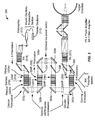
- FIG. 3 is a simplified unfolded view of a multi-pass amplifier 300 according to an embodiment of the present invention.
- light from a master oscillator 310 and preamplifier 312 is injected into the power amplifier 314 in the S-polarization: Injection of a first beamline with S-polarization (also referred to as horizontal polarization) may occur just before the pinhole plane of TSF that is utilized in conjunction with the multi-pass amplifier 300.
- Light enters the first amplifier module including slablets 316 and passes through a quarter wave plate (QWP) 318 that converts the S-polarized light into circularly polarized light.
- QWP quarter wave plate
- the circularly polarized light passes through the slablets 316 positioned at normal incidence, in contrast with designs using slabs at Brewster's angle.
- the slablets 316 are positioned between windows 320a and 320b in order to enable cooling of the slablets 316 using helium or other suitable coolant gas as discussed above.
- Passing through the amplifier/gain slablets also referred to as amplifier slabs, gain slabs, or slablets
- amplifier slabs, gain slabs, or slablets where the beamline experiences gain at normal incidence provides the benefit of reducing the non-linear index by a factor of 2/3 from the original value, thereby decreasing the ⁇ B.
- amplifier modules that can be referred to as a "Normal Amplifier" because light is incident on the amplifier slablets at normal incidence.
- the Normal Amplifier (also referred to as an amplifier module) includes a plurality of amplifier slablets 316, a quarter-wave plate 318 and optional windows 320a/b that are all nominally positioned at normal incidence to the beams that propagate through them.
- the number of slablets in each amplifier module can range from about 10 slablets to about 100 slablets. In a specific embodiment, between 50 and 60 slablets are utilized.
- an amplifier module After the pass through the first amplifier module, the beam is reflected into the second amplifier module using, for example, a set of reflectors 325a and 325b that may be dielectric mirrors or angle discriminating reflectors.
- the second and subsequent amplifier modules share common elements with the first amplifier module. Similar elements may or may not be discussed in the description that follows for purposes of clarity and conciseness.
- an amplifier module includes a set of windows (which may be commonly shared with other amplifier modules as described below), a QWP, and a set of amplifier slablets.
- the amplifier module may include other elements as appropriate to the particular application.
- One of ordinary skill in the art would recognize many variations, modifications, and alternatives.
- the QWP 332 converts the light to P-polarization (also referred to as vertical polarization) as illustrated in FIG. 3 .
- the light then passes through a polarizer 334 aligned to pass the P-polarization state and is reflected by a set of mirrors 336a and 336b as discussed below.
- This set of mirrors can be dielectric mirrors, angle discriminating reflectors, or the like.
- the light (in the P-polarization state) passes through another polarizer 338 and propagates to the entrance of a third amplifier module.
- a QWP is positioned at the entrance to the third amplifier module, in order to convert the light from the P-polarization state to circular polarization.
- the light is circularly polarized as illustrated in FIG. 3 .
- Another set of mirrors 342a and 342b which may be dielectric mirrors, angle discriminating reflectors, or the like, is utilized to form an optical path between the third and fourth amplifier modules. Light is converted back to S-polarization by the QWP 350 in the fourth amplifier module, exiting after the fourth amplification pass in the S-polarization.
- the S-polarized light reflects off a polarizer 360 and a mirror 362, where it is directed toward the PA 370, which may include a set of amplifier slabs (or slablets) oriented at Brewster's angle.
- the PA 370 may include a set of amplifier slabs (or slablets) oriented at Brewster's angle.
- slablets only a single set of windows is used for each amplifier module, rather than a set of windows for every slab.
- multiple amplifier modules may be combined in a single cooling enclosure, which may reduce the number of windows.
- power amplifier 314 and power amplifier 370 are a same power amplifier operable to provide initially amplified light to the first amplifier module and to receive amplified light from the fourth amplifier module.
- the main amplifier (MA) amplifier section includes the four amplifier modules discussed above.
- a fourth beamline can be injected into the TSF at the bottom of FIG. 3 , propagating in the reverse direction at a small angle with respect to the first beamline illustrated in FIG. 3 .
- Optional birefringence compensators can be placed between the first and second amplifier modules as well as between the third and fourth amplifier modules to compensate for birefringence accumulated in the amplified beams. Both birefringence compensators are optional. Additionally, it is possible to insert a "low power" switch between the second amplifier module and the third amplifier module. The term "low power" is used in comparison to the beam intensity after the pass through the fourth amplifier module. Since the optional switch can be utilized after the second amplifier module, the power is significantly less than after the fourth amplifier module, enabling switches to be used that are suitable for use at lower powers than associated with the amplification pass through the fourth amplifier module.
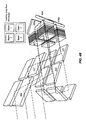
- FIG. 4A is a three dimensional view of a multi-pass amplifier system 400 illustrated according to an embodiment of the present invention.
- the architecture illustrated in FIG. 4A is related to the unfolded architecture illustrated in FIG. 3 .
- the amplifier system illustrated in FIG. 4A provides a "quad" of four normal incidence amplifier modules 460, 461, 462, and one not shown) in which the amplified beams share components.
- the multi-pass amplifier illustrated in FIG. 4A does not include the master oscillator 310, preamplifier 312, or power amplifiers 314/370 illustrated in FIG. 3 . Of course, depending on the particular implementation, these additional optical systems may be integrated with the multi-pass amplifier.
- the elements illustrated in FIG. 4A may also be referred to as a main amplifier system 400.
- the multi-pass amplifier system 400 (for example, through Aperture 1) as S-polarized light and reflects off mirror 410.
- the S-polarized light is then reflected off of polarizer 420 toward the first amplifier module 460, which includes a set of windows surrounding a QWP and a plurality of amplifier slablets (See, for example, FIG. 3 for additional description related to amplifier modules).
- the light passes through the QWP and is converted to circular polarization.
- the second amplifier module 461 also includes a QWP, for example, at the end opposing mirror 450b, which converts the light to P-polarization.
- the light (after two amplification passes), passes through a polarizer (not shown) positioned under polarizer 420 and reflects off a set of 45° mirrors (not shown). The light then passes through a polarizer (not shown) that is positioned below polarizer 422 and aligned with the P-polarized light. Because of the three-dimensional nature of the amplifier architecture, consideration of both FIG. 3 and FIG. 4A in conjunction with each other is helpful in understanding embodiments of the present invention.
- the light them makes two more amplification passes, first through a third amplifier module (not shown) and fourth amplifier module 462.
- the third and fourth amplifier modules include a QWP on the side opposing 45 mirror set 456, which converts the light from P-polarization to circular polarization (during amplification) and then to S-polarization.
- the S-polarized light exiting the fourth amplifier module 462 reflects off polarizer 422 toward mirror 412, where it is reflected out of the main amplifier system.
- a switch can optionally be used, for example, after the second amplification pass, to improve system performance.
- each beamline will enter at one aperture and exit at another.
- a beam entering Aperture 4 will exit at Aperture 1.
- the beams can be canted at a small angle (e.g., 1 mrad) with respect to each other to provide multiple passes propagating along slightly different beam paths.
- the beams can be canted at other angles, for example, angles ranging from about 1 mrad to about 3 mrad or less than 1 mrad.
- embodiments of the present invention provide an amplifier architecture having a four pass geometry in which each beam only makes a single pass through each amplifier module. Additionally, no polarization switch is used in the embodiment illustrated in FIG. 4 .
- four beams are amplified as each of the four beams makes a pass through each of the four amplifier modules (i.e., four beams and four pass amplification for each beam), which is suitable to provide high power output with a reasonable size front end.
- four beams are amplified as each of the four beams makes a pass through each of the four amplifier modules (i.e., four beams and four pass amplification for each beam), which is suitable to provide high power output with a reasonable size front end.
- One of ordinary skill in the art would recognize many variations, modifications, and alternatives.
- four beamlines are utilized:
- Embodiments of the present invention provide benefits not available using conventional architectures including the reduction of the number of telescopes used along the optical path.
- the telescope that serves as the cavity spatial filter (CSF) is not present in the architecture illustrated in FIG. 3 .
- the CSF relays an image plane about 22 meters (equal to the length of the CSF telescope) for an overall optical cavity length of 44 meters, whereas in some embodiments, the entire main amplifier system illustrated in FIG. 4 is packed into a module about 6 meters in length. Additionally, vignetting losses are reduced by embodiments of the present invention in comparison with conventional architectures.
- Beam cleanup can be performed in some embodiments using only the TSF and/or narrow range angular coatings on the mirrors or other optical elements present in the system.
- angle discriminating coatings can be utilized on one or more reflective or transmissive optics along the beam path including mirrors and/or polarizers.
- a variety of bulk angular discriminating optics are available as options and the filtering does not have to occur at the focal point, but discrimination can be performed at large apertures, either as a coating or as bulk material, where it is easier to dissipate heat.
- using large aperture angular discrimination can reduce the loads of any other spatial filters that are used in the system, if spatial filters are used.
- the four amplifier modules illustrated in FIG. 4A can be packaged in two or more separate cooling enclosures or in a single cooling enclosure as appropriate to the particular application.
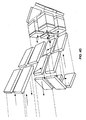
- FIG. 4B is a three dimensional perspective diagram illustrating ray trace paths through a multi-pass amplifier according to an embodiment of the present invention.
- the three dimensional perspective diagram illustrated in FIG. 4B shares some common components with that illustrated in FIG. 4A .
- the amplifier modules may also be coupled by the 45 degree mirrors oriented to provide two amplification passes in a horizontal plane (e.g., Beam 1 and Beam 2), rather than the vertical plane illustrated in FIG. 4A . Accordingly, light passing through amplifier module 471 is reflected toward amplifier module 470 by reflectors 450e and 450f.
- FIG. 4C is a three dimensional perspective view of multi-pass amplifier viewed from a first direction according to an embodiment of the present invention.
- FIG. 4D is a three dimensional perspective view of a multi-pass amplifier viewed from a second direction according to an embodiment of the present invention.
- the multi-pass amplifiers illustrated in FIGS. 4C and 4D share common components with the amplifier systems illustrated in FIGS. 4A and 4B and are not labeled for purposes of clarity and conciseness.
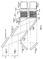
- FIG. 5 is a simplified schematic diagram illustrating a top half of a multi-pass amplifier according to an embodiment of the present invention. As described below, two additional amplifier modules (not shown) complete a four amplifier module system in some embodiments. In FIG. 5 , a single beamline of a quad of beamlines are illustrated, showing two amplifier modules 560 and 562 (Normal Amplifiers). These Normal Amplifiers can be compared to the first and second amplified modules discussed in FIG. 3 .
- Light enters the amplifier system with an S-polarization (570), reflects of mirror 510 and off of polarizer 520. The input light passes through one of the windows (window 565) surrounding the quarter wave plate (QWP) 530 and the set of amplifier slablets 540.
- S-polarization 570
- the input light passes through one of the windows (window 565) surrounding the quarter wave plate (QWP) 530 and the set of amplifier slablets 540.
- QWP quarter wave plate
- the QWP 530 converts the light with S-polarization to circular polarization and the beam is amplified by the amplifier slablets 540.
- the light is substantially at normal incidence to the QWP and the amplifier slablets in the first amplifier module 560.
- the light is reflected by the 45 degree mirror 550 to a second amplifier module (not shown) behind the plane of the figure.
- the light makes a second amplification pass and is converted to P-polarization by the QWP in the second amplifier module. Because the light is in the P-polarization state, it passes through polarizer 520, which extends into and behind the plane of the figure, and is reflected off 45 degree mirrors 552 and 554.
- Polarizer 520 could also be two polarizers that are stacked along a line normal to the plane of the figures.
- the light in the P-polarization state passes through polarizer 522 (extending behind the plane of the figure or a polarizer positioned behind the plane of the figure) and enters a third amplifier module (not shown) behind the plane of the figure.
- the QWP in the third amplifier module converts the light to circular polarization and after amplification, the light is reflected by 45 degree mirror set 566 to impinge on the fourth amplifier module 562. After the fourth amplification pass, the light is converted to S-polarization by QWP 514 and is reflected from polarizer 522 and mirror 512 to exit the system.
- entrance aperture 570 is labeled as “In” and exit aperture 572 is labeled as “Out,” it will be appreciated that in a multi-beam system (e.g., a four beam system), a second beamline will be entering at aperture 572 and exiting at aperture 570. Thus, "In” and “Out” are only applicable to one of the multiple beamlines.
- FIG. 6 is a simplified schematic diagram illustrating a top half of a multi-pass amplifier including a polarization switch according to an embodiment of the present invention.
- the multi-pass amplifier system illustrated in FIG. 6 shares common elements with the multi-pass amplifier system illustrated in FIG. 5 and common elements are not necessarily described for purposes of clarity and conciseness.
- switch 605 which may be a half-wave switch such as a PEPC, is inserted in the optical path after the light has traveled through two of the amplifier modules. In an "off" state, the half-wave switch would act as a half wave plate, thereby blocking transmission of light through the system.
- the switch When the extraction pulse is due, the switch will be energized to the "on" state, in which state the switch would be a zero-wave plate, thereby permitting the extraction pulse to pass through the polarizers aligned with the polarization of the pulse.
- the switch is shown in the plane containing the two amplifier modules 360 and 362, it will be appreciated that a switch in the top plane will be active for the beamlines starting and ending in the plane positioned behind the plane of the figure. The switch for the beamlines entering and exiting in the plane of the figure will be placed in the plane behind the figure.
- switch 605 Placement of switch 605 at a position between the second and third amplifier modules enables amplified spontaneous emission (ASE) and other undesired light (stray light from glints) that can reduce the amplification efficiency to be blocked after at most two passes through the amplifier modules.
- ASE amplified spontaneous emission
- other undesired light stray light from glints
- the fluences associated with two passes is less than or equal to about 100 Joules. Therefore, the fluence experienced by switch 605 is much less than the fluence experienced by the polarization switch illustrated in FIG. 1 . Comparing FIGS. 1 and 6 , the placement of the polarization switch in FIG. 1 results in an exposure to the full fluence associated with four amplification passes ( ⁇ 10 KJ), several orders of magnitude greater than the fluence after two amplification passes that is experienced by switch 605.
- the lower power experienced by switch 605 enables the use of multiple options for switching, including Pockels cell, employing a transparent electrode made, for example, using indium/tin/oxide coatings (see, for example, W.T. Pawlewicz, I.B.Mann, W.H. Lowdermilk and D. Milam, Laser-damage -resistant transparent conductive indium tin oxide coatings, Appl. Phys. Lett. 34(3), 1 Feb. 1979 ) as demonstrated at centimeter scale (see, for example, M.D. Skeldon, M.S. Jin D.J. Smith and S.T. Bui, Performance of longitudinal mode KDP Pockels cells with transparent conductive electrodes, SPIE Vol. 1410 Solid State Lasers II (1991 )), other suitable transparent electrodes, or the like.
- indium/tin/oxide coatings see, for example, W.T. Pawlewicz, I.B.Mann, W.H. Lowdermilk and D. Milam, Laser-damage
- FIG. 7 is a side view of a multi-pass amplifier including a pump light injection system according to an embodiment of the present invention.
- the multi-pass amplifier illustrated in FIG. 7 shares common elements with the multi-pass amplifier system illustrated in FIG. 5 and common elements are not necessarily described for purposes of clarity and conciseness.
- Amplifier modules and 45° mirror sets to direct the beam into the set of amplifier modules behind the plane of the figure are illustrated in FIG. 7 .
- pump light is injected using dichroic mirrors to enable face pumping of the amplifier slablets along a direction aligned with the light beam to be amplified (normal incidence).
- the positions of the polarizers and mirrors used to direct the amplified beams can be adjusted to allow for the placement of the dichroic mirrors 710 used to pump the gain media.
- the design illustrated in FIG. 7 enables the pump light to reach the gain media while still maintaining high efficiency for the amplified light beams.
- Optical concentrators or ducts of various types may be used to direct the diode pump light into the amplifier end faces and/or edges. Both the lasant concentrations and slablet thicknesses may be varied along the length of the amplifier assembly in order to hold thermally induced phase distortion and thermally induced stress birefringence within acceptable tolerances.
- FIG. 8 is a perspective drawing illustrating a method of gap pumping amplifier slablets according to an embodiment of the present invention.
- a single amplifier slablet is illustrated, although multiple slablets will typically be utilized as illustrated in FIG. 3 and other figures described herein.
- a fin 810 that is shaped in a generally conical shape is attached to the top surface of the amplifier slablet 820.
- a similar fin 811 is attached to the bottom edge of the amplifier slablet.
- the fins provide an aerodynamic environment that enhances the flow of the high pressure helium used as the cooling fluid. In the illustrated embodiment, the helium is flowing up past the amplifier slablet 820 and fins 810 and 811.
- the amplifier slablet has an edge cladding 830 positioned around the edges of the amplifier slablet for collecting the ASE that propagates across the slablets.
- the edge cladding 830 is cooled in the illustrated embodiment by circulating water through the edge cladding cooling channels 832.
- Pump light is injected through ducts 840 in a direction perpendicular to the direction of propagation of the amplified light.
- the ducts separate the slablets from each other, with a gap between the slablets through which the cooling gas flows.
- the ducts 840 are characterized by predetermined dimensions, for example, plates approximately 3 mm thick and approximately 40 cm long.
- the ducts overlap with the edge cladding and form spacers between the slablets.
- the pump light exits the duct on the inner surfaces of the ducts positioned between the slablets and propagates into the region between adjacent slablets. Because the pump light diffracts as it exits the duct, or by design of the duct surface, the pump light enters the gap region with a spread of angles. As the light in the lower index region between amplifier slablets impinges on the higher index slablets, the pump light is coupled into the amplifier slablets, providing gain.
- the faces of the amplifier slablets can be etched or otherwise enhanced to increase the coupling of the pump light from the gap region into the amplifier slablets.
- the amplifier slablets can be AR coated for normal incidence light using etching, by a solgel layer, or the like, they can absorb the pump light through these faces.
- the faces of the slablets could be etched with an irregular pattern or other suitable treatment to increase the coupling of the pump light into the amplifier slablets by scattering, deflection, or the like.
- the output surfaces of the ducts 840 can be angled to match the numerical aperture of the duct to the amplifier slablet coupling coefficient to provide for uniform absorption of the pump light across the amplifier slablet.
- structures that scatter mildly when viewed from an angle and act as an AR coating at normal incidence can be used that couple the pump light into the amplifier slablets effectively while still providing high quality coatings in terms of damage performance.
- Fiber couplers joined to semiconductor lasers can also be utilized according to some embodiments to replace or supplement the ducts 840.
- FIG. 9 is a simplified schematic diagram illustrating a two-pass amplifier architecture according to an embodiment of the present invention.
- a two-pass architecture can be implemented that does not include a switch (e.g., a PEPC) to prevent ASE or a large aperture Faraday rotator.
- the amplifier slablets utilized in FIG. 9 can be positioned to receive light at substantially normal incidence (not at Brewster's angle) and anti-reflection (AR) coated or may be positioned to receive light at Brewster's angle and not be AR coated.
- FIG. 10 is a simplified schematic diagram illustrating integration of a set of two-pass amplifier architectures according to an embodiment of the present invention. In the embodiment illustrated in FIG. 10 , two two-pass beamlines can be stacked and shared such that the laser pulses do not traverse the same optical element more than once.
- light enters the system through the TSF 910 in the S-polarization.
- the light is amplified by the power amplifier 912, which in the illustrated embodiment, includes a plurality of slablets positioned at Brewster's angle.
- the input light reflects off the polarizer 920, which is aligned to reflect light in the S-polarization and pass light in the P-polarization.
- the reflected light is then is converted into circular polarization by the QWP 922.
- the second pass through the QWP 922 converts the light to the P-polarization, which enables the light to pass through the polarizer 920 and enter the CSF 930.
- the CSF which is optional in some embodiments, filters the light to improve the beam quality.
- the light in the P-polarization makes a first pass through the main amplifier 932, which includes a plurality of slablets oriented at Brewster's angle in the illustrated embodiment. After reflection off mirror 934, the light makes a second pass through the main amplifier 932 to achieve two amplification passes.
- the amplified light passes through the optional CSF 930, the polarizer 920 and is converted into circularly polarized light by the QWP 922. After a final reflection off of mirror 924, the QWP converts the light to S-polarization, which reflects off the polarizer 920 toward mirror 914 as it begins the exit from the amplifier system.
- the light in the S-polarization reflects off polarizer 1024 and makes two passes through the QWP 1022 (before and after reflection off of mirror 1020), converting the light in the S-polarization state into P-polarization.
- the light them passes through the polarizer 1024 and is amplified during the pass through main amplifier 1026.
- the light is then directed toward the second main amplifier 1036 after reflection from mirrors 1028 and 1038.
- each amplifier is a single pass amplifier for the beamline illustrated in FIG. 10 .
- another beamline can propagate from the output to the input in the reverse direction.
- FIG. 11 is a simplified schematic diagram illustrating a single aperture four pass amplifier design with a "low power" PEPC. As discussed above, the term “low power” is in comparison to the final output power of optical systems described herein.
- the amplifier illustrated in FIG. 11 shares common elements with the amplifier system illustrated in FIG. 9 and common elements are not necessarily described or numbered for purposes of clarity and conciseness.
- light to be amplified is injected in the S-polarization and reflects off the polarizer toward the QWP, which converts the light to circular polarization. The light passes through the slablets during a first amplification pass and passes through an optical birefringence compensator.
- the light is reflected back through the optional birefringence compensator prior to a second amplification pass through the slablets.
- the QWP will convert the polarization to the P-polarization so that the light (having had two amplification passes) passes through the polarizer toward the low power switch.
- the switch is operated to pass the light so that it can be reflected back toward the slablets. After the light passes through the switch after reflection, the switch can be closed.
- FIG. 12 is an unwound version of the system illustrated in FIG. 11 , illustrating the optical path during the four amplification passes.
- the low power switch enables suppression of parasitic modes to be performed using an electro-optic switch operating at power levels less than that of the final amplified beam. In the embodiment illustrated in FIGS. 11 and 12 , the parasitic mode suppression is performed after two of four amplification passes.
- the embodiments illustrated in FIGS. 9-12 may not utilize the three-dimensional architecture discussed in relation to FIGS. 4A-4D , but may be characterized by a two-dimensional architecture in the sense that amplifier modules are not necessarily arrayed in two dimensions.
- the amplifier modules are arrayed as a 2x2 array in a plane substantially orthogonal to the direction of propagation of the light being amplified in the amplifier modules.
- This geometry may not be needed in the embodiments illustrated in FIGS. 9-12 .
- the embodiments illustrated in FIGS. 9-12 may be considered as a subset of the more general three-dimensional geometries illustrated in FIGS. 4A-4D .
- One of ordinary skill in the art would recognize many variations, modifications, and alternatives.
- birefringence compensators as indicated in FIGS. 3 and 11 .
- Stress induced birefringence may cause spatially dependent depolarization of the laser pulses passing through the laser amplifiers.
- the addition of a compensator plate may be required to reverse the sign of the depolarization between amplifier passes so as to allow the identically distorted following amplifier to correct the polarization state.
Landscapes
- Physics & Mathematics (AREA)
- Electromagnetism (AREA)
- Engineering & Computer Science (AREA)
- Plasma & Fusion (AREA)
- Optics & Photonics (AREA)
- Chemical & Material Sciences (AREA)
- Crystallography & Structural Chemistry (AREA)
- Lasers (AREA)
Claims (17)
- Système amplificateur optique (400) comprenant :- un premier réflecteur (410 ; 510 ; 610) utilisable pour recevoir une lumière d'entrée à travers une première ouverture et diriger la lumière d'entrée le long d'un trajet optique, dans lequel la lumière d'entrée est caractérisée par un état de polarisation (S) ;- un premier polariseur (420 ; 520) utilisable pour réfléchir la lumière ayant l'état de polarisation (S) le long du trajet optique ;- un premier ensemble de modules amplificateurs (460, 461 ; 470, 471 ; 560) disposés le long du trajet optique, comprenant un premier module amplificateur (460 ; 470 ; 560) et un deuxième module amplificateur (461 ; 471) ;- un second ensemble de modules amplificateurs (462 ; 472 ; 562) disposés le long du trajet optique, comprenant un troisième module amplificateur et un quatrième module amplificateur (462 ; 472 ; 562) ;- un ensemble de miroirs (450a, 450b, 450f, 450e ; 550) utilisable pour réfléchir la lumière sortant du premier module amplificateur pour entrer dans le deuxième module amplificateur, chaque amplificateur ayant à chaque extrémité une fenêtre ;- un ensemble de miroirs (552, 554) utilisable pour réfléchir la lumière sortant du premier ensemble de modules amplificateurs (460, 461 ; 470, 471 ; 560) pour qu'elle entre dans le second ensemble de modules amplificateurs (462 ; 472 ; 562) ;- un deuxième polariseur (422 ; 522 ; 622) utilisable pour réfléchir la lumière ayant un état de polarisation (S) le long du trajet optique ; et- un second réflecteur (412 ; 512) utilisable pour réfléchir la lumière amplifiée réfléchie à partir du deuxième polariseur (422 ; 522) ;dans lequel les modules amplificateurs sont disposés selon une géométrie tridimensionnelle, les fenêtres d'extrémité de chaque amplificateur étant sensiblement situées dans deux plans, parallèles l'un à l'autre.
- Système amplificateur selon la revendication 1, étant un système amplificateur principal (AP), dans lequel chacun du premier ensemble de modules amplificateurs (460, 461 ; 470, 471 ; 560) comprend :- une fenêtre d'entrée (320a ; 565) ;- une plaque quart d'onde (318, 332 ; 530 ; QWP) ;- une pluralité de petites plaques amplificatrices (316, 330 ; 540) disposées de manière sensiblement parallèle les unes par rapport aux autres ; et- une fenêtre de sortie (320b) ; et- dans lequel chacun du second ensemble de modules amplificateurs (462 ; 472 ; 562) comprend :- une fenêtre d'entrée ;- une plaque quart d'onde (340, 350 ; 514 ; QWP) ;- une pluralité de petites plaques amplificatrices disposées de manière sensiblement parallèle les unes par rapport aux autres ; et- une fenêtre de sortie.
- Système amplificateur principal selon la revendication 2, comprenant en outre une plaque correctrice utilisable pour atténuer au moins l'une d'une erreur de phase ou de polarisation.
- Système amplificateur principal selon la revendication 2, dans lequel la pluralité de modules amplificateurs comprend quatre modules amplificateurs (460, 461, 462 ; 470, 471, 472 ; 560, 562).
- Système amplificateur principal selon la revendication 2, dans lequel chacun de la pluralité de modules amplificateurs est refroidi par l'écoulement d'un gaz, le gaz comprenant éventuellement de l'hélium.
- Système amplificateur principal selon la revendication 2, dans lequel le premier réflecteur (410 ; 510 ; 610) comprend un réflecteur d'entrée pour une première ligne de faisceau (faisceau 1) et un réflecteur de sortie pour une seconde ligne de faisceau (faisceau 4).
- Système amplificateur principal selon la revendication 2, comprenant en outre un interrupteur (605) positionné entre deux miroirs (552, 554) de l'ensemble de miroirs.
- Système amplificateur selon la revendication 2, dans lequel l'état de polarisation comprend une polarisation S.
- Système amplificateur selon la revendication 2, dans lequel une ligne de faisceau (faisceau 1) du système amplificateur (400) comprend le trajet optique allant de la première ouverture à la seconde ouverture différente de la première ouverture.
- Système amplificateur optique selon la revendication 1, dans lequel l'amplificateur comprend un amplificateur à deux passes (1026, 1036).
- Système amplificateur optique selon la revendication 1, dans lequel l'amplificateur (400) comprend une pluralité de petites plaques utilisables pour recevoir un écoulement de gaz de refroidissement entre la pluralité de petites plaques.
- Procédé d'amplification d'une impulsion d'entrée, le procédé comprenant :- la réception, à travers une première ouverture, d'une impulsion d'entrée ayant un premier état de polarisation (S) le long d'une ligne de faisceau d'entrée (faisceau 1) d'un système amplificateur (400) ;- la réflexion de l'impulsion d'entrée à partir d'un miroir d'entrée (410 ; 510 ; 610) ;- la réflexion de l'impulsion d'entrée à partir d'un premier polariseur (420 ; 520) en conséquence du fait que l'impulsion d'entrée a le premier état de polarisation (S) ;- la conversion du premier état de polarisation (S) en un premier état de polarisation intermédiaire ;- l'amplification de l'impulsion d'entrée en utilisant un premier ensemble de modules amplificateurs (460, 461 ; 470, 471 ; 560) pour fournir une impulsion amplifiée ayant le premier état de polarisation intermédiaire, ledit premier ensemble de modules amplificateurs comprenant un premier module amplificateur (460 ; 470 ; 560) et un second module amplificateur (461 ; 471), l'impulsion sortant dudit premier module amplificateur étant réfléchie par un ensemble de miroirs (450a, 450b ; 450f, 450e ; 550) utilisable pour réfléchir la lumière sortant du premier module amplificateur pour entrer dans le second module amplificateur, chaque amplificateur ayant à chaque extrémité une fenêtre ;- la conversion de l'impulsion amplifiée ayant le premier état de polarisation intermédiaire en une impulsion amplifiée ayant un second état de polarisation (P) ;- le passage de l'impulsion amplifiée à travers un deuxième polariseur en conséquence du fait que l'impulsion amplifiée a le second état de polarisation (P), l'impulsion sortant dudit deuxième polariseur étant réfléchie par un ensemble de miroirs (552, 554) utilisables pour réfléchir la lumière sortant du premier ensemble de modules amplificateurs pour qu'elle entre dans le second ensemble de modules amplificateurs ;- le passage de l'impulsion amplifiée à travers un troisième polariseur en conséquence du fait que l'impulsion amplifiée a le second état de polarisation (P) ;- la conversion du second état de polarisation (P) en un second état de polarisation intermédiaire ;- l'amplification de l'impulsion amplifiée en utilisant un second ensemble de modules amplificateurs (462 ; 472 ; 562) pour fournir une impulsion de sortie ayant le second état de polarisation intermédiaire, ledit second ensemble de modules amplificateurs comprenant un troisième module amplificateur et un quatrième module amplificateur (462 ; 472 ; 562), l'impulsion sortant dudit troisième module amplificateur étant réfléchie par un ensemble de miroirs (456b, 456a ; 456g ; 556) utilisable pour réfléchir la lumière sortant du troisième module amplificateur pour qu'elle entre dans le quatrième module amplificateur, chaque amplificateur ayant à chaque extrémité une fenêtre ;- la conversion du second état de polarisation intermédiaire en le premier état de polarisation (S) ;- la réflexion de l'impulsion de sortie à partir du polariseur (422 ; 522 ; 622) en conséquence du fait que l'impulsion de sortie a le premier état de polarisation (S) ;- la réflexion de l'impulsion amplifiée à partir d'un miroir de sortie (412 ; 512) ; et- la direction de l'impulsion de sortie ayant le premier état de polarisation (S) le long d'une ligne de faisceau sortant ((faisceau 4) du système amplificateur (400), à travers une seconde ouverture, ladite ligne de faisceau sortant étant différente de la ligne de faisceau entrant ; et dans lequel les modules amplificateurs sont disposés selon une géométrie tridimensionnelle, les fenêtres d'extrémité de chaque amplificateur étant placées sensiblement dans deux plans, parallèles l'un à l'autre.
- Procédé selon la revendication 12, dans lequel la conversion du premier état de polarisation (S) en le premier état de polarisation intermédiaire comprend le passage de l'impulsion d'entrée à travers une plaque quart d'onde (318, 332 ; 530 ; QWP).
- Procédé selon la revendication 12, dans lequel l'amplification de l'impulsion d'entrée pour fournir une impulsion amplifiée comprend le passage de l'impulsion d'entrée à travers une pluralité de petites plaques amplificatrices (316, 330 ; 540) à un angle d'incidence sensiblement normal.
- Procédé selon la revendication 12, dans lequel la ligne de faisceau (faisceau 1) du système amplificateur (400) comprend un trajet optique allant de la première ouverture à la seconde ouverture différente de la première ouverture.
- Procédé selon la revendication 12, dans lequel le premier état de polarisation comprend une polarisation S et le second état de polarisation comprend une polarisation P.
- Procédé selon la revendication 12, dans lequel le premier état de polarisation comprend une polarisation circulaire ayant un premier sens de rotation et le second état de polarisation intermédiaire comprend une polarisation circulaire ayant un second sens de rotation opposé au premier sens de rotation.
Applications Claiming Priority (2)
| Application Number | Priority Date | Filing Date | Title |
|---|---|---|---|
| US31813610P | 2010-03-26 | 2010-03-26 | |
| PCT/US2011/030081 WO2011120009A1 (fr) | 2010-03-26 | 2011-03-25 | Architecture d'amplificateur à passes multiples pour systèmes laser à haute puissance |
Publications (3)
| Publication Number | Publication Date |
|---|---|
| EP2553778A1 EP2553778A1 (fr) | 2013-02-06 |
| EP2553778A4 EP2553778A4 (fr) | 2013-08-28 |
| EP2553778B1 true EP2553778B1 (fr) | 2015-12-09 |
Family
ID=44673667
Family Applications (1)
| Application Number | Title | Priority Date | Filing Date |
|---|---|---|---|
| EP11760349.8A Active EP2553778B1 (fr) | 2010-03-26 | 2011-03-25 | Architecture d'amplificateur pour systèmes laser à haute puissance |
Country Status (7)
| Country | Link |
|---|---|
| US (1) | US8687270B2 (fr) |
| EP (1) | EP2553778B1 (fr) |
| JP (1) | JP5933521B2 (fr) |
| KR (2) | KR101862418B1 (fr) |
| CN (1) | CN102870293A (fr) |
| RU (1) | RU2589274C2 (fr) |
| WO (1) | WO2011120009A1 (fr) |
Cited By (1)
| Publication number | Priority date | Publication date | Assignee | Title |
|---|---|---|---|---|
| US11329448B2 (en) | 2017-05-24 | 2022-05-10 | United Kingdom Research And Innovation | Laser amplifier module |
Families Citing this family (9)
| Publication number | Priority date | Publication date | Assignee | Title |
|---|---|---|---|---|
| JP2013135075A (ja) * | 2011-12-26 | 2013-07-08 | Gigaphoton Inc | 固体レーザ増幅器、レーザ光増幅器、固体レーザ装置、およびレーザ装置 |
| US9537282B2 (en) * | 2013-09-20 | 2017-01-03 | Alcatel Lucent | System and method for a multi-mode pump in an optical amplifier |
| US9160136B1 (en) * | 2014-05-30 | 2015-10-13 | Lee Laser, Inc. | External diffusion amplifier |
| US9899798B2 (en) | 2015-08-03 | 2018-02-20 | University Of Central Florida Research Foundation, Inc. | Apparatus and method for suppressing parasitic lasing and applications thereof |
| EP3622593A4 (fr) * | 2017-05-08 | 2021-01-06 | Lawrence Livermore National Security, LLC | Mise à l'échelle de lasers à semi-conducteurs pulsés à haute énergie à une puissance moyenne élevée |
| CN107104350B (zh) * | 2017-05-25 | 2023-07-28 | 衢州学院 | 一种激光放大器 |
| RU2703937C1 (ru) * | 2018-12-11 | 2019-10-22 | Федеральное государственное бюджетное научное учреждение "Федеральный исследовательский центр Институт прикладной физики Российской академии наук" (ИПФ РАН) | Способ увеличения частоты следования ультракоротких высокомощных лазерных импульсов в ограниченной последовательности |
| CN112018587B (zh) * | 2020-07-27 | 2022-06-03 | 横琴东辉科技有限公司 | 一种抑制sbs实现高功率单频光纤激光输出的方法 |
| CN116435857B (zh) * | 2023-04-04 | 2025-07-25 | 中国工程物理研究院激光聚变研究中心 | 一种光束偏振可控装置、热退偏补偿系统及使用方法 |
Family Cites Families (54)
| Publication number | Priority date | Publication date | Assignee | Title |
|---|---|---|---|---|
| US3798571A (en) * | 1969-06-09 | 1974-03-19 | American Optical Corp | Slab laser system with means to overcome the positive lens effect caused by the thermal gradient in the laser rod |
| AU463106B2 (en) * | 1973-02-09 | 1975-07-17 | Leonard Hughes John | Laser amplifier |
| US4132955A (en) * | 1974-08-01 | 1979-01-02 | Helen Hughes | System for amplifying laser beams |
| US4039962A (en) * | 1974-08-01 | 1977-08-02 | John Leonard Hughes | System for amplifying laser beams |
| FR2402956A1 (fr) * | 1977-09-08 | 1979-04-06 | Comp Generale Electricite | Chaine d'amplification laser |
| US4698816A (en) | 1982-12-20 | 1987-10-06 | General Electric Co. | Optical transmission filter |
| US4575849A (en) * | 1982-12-20 | 1986-03-11 | General Electric Company | Optical filter polarizer combination and laser apparatus incorporating this combination |
| US4563763A (en) | 1983-08-22 | 1986-01-07 | Board Of Trustees, Leland Stanford University | Method and apparatus for cooling a slab laser |
| US4559627A (en) * | 1984-06-18 | 1985-12-17 | General Electric Company | Face pumped rectangular slab laser apparatus having an improved optical resonator cavity |
| US4642809A (en) * | 1985-02-28 | 1987-02-10 | Rca Corporation | Slab active lasing medium |
| US4682340A (en) * | 1985-12-30 | 1987-07-21 | Gte Government Systems Corporation | Apparatus for and method of extracting an output beam from a laser system |
| US4734911A (en) * | 1986-03-14 | 1988-03-29 | Hughes Aircraft Company | Efficient phase conjugate laser |
| US4969169A (en) * | 1986-04-15 | 1990-11-06 | Hampshire Instruments, Inc. | X-ray lithography system |
| US4725787A (en) * | 1986-12-31 | 1988-02-16 | The United States Of America As Represented By The Secretary Of The Army | Phase-conjugated hybrid slab laser |
| US4918395A (en) * | 1988-11-21 | 1990-04-17 | Spectra-Physics | Multipass laser amplifier with at least one expanded pass |
| US4837769A (en) * | 1989-02-01 | 1989-06-06 | The United States Of America As Represented By The Secretary Of The Army | Phase conjugated slab laser designator |
| US4989216A (en) * | 1990-04-18 | 1991-01-29 | The United States Of America As Represented By The Secretary Of The Army | Double conjugate laser amplifier |
| US5018163A (en) * | 1990-04-26 | 1991-05-21 | The United States Of America As Represented By The Secretary Of The Army | Gatling gun laser pulse amplifier using an optical diode |
| US5260954A (en) * | 1992-10-29 | 1993-11-09 | The Unived States Of America As Represented By The United States Department Of Energy | Pulse compression and prepulse suppression apparatus |
| US5268787A (en) * | 1993-02-17 | 1993-12-07 | Energy Compression Research Corp. | Multiple-pass method and apparatus for laser amplification |
| US5469454A (en) * | 1994-05-02 | 1995-11-21 | University Of Central Florida | Mode locked laser diode in a high power solid state regenerative amplifier and mount mechanism |
| US5742634A (en) | 1994-08-24 | 1998-04-21 | Imar Technology Co. | Picosecond laser |
| KR0149771B1 (ko) * | 1995-07-28 | 1998-12-01 | 윤덕용 | 고반복, 고에너지 및 고출력 레이저 빔 발생용 고체 레이저 |
| JP3588195B2 (ja) * | 1996-07-18 | 2004-11-10 | 浜松ホトニクス株式会社 | 固体レーザ増幅器 |
| IL126915A (en) * | 1998-11-05 | 2002-09-12 | Elop Electrooptics Ind Ltd | System and sailing for amplifying a laser beam |
| WO2001003260A1 (fr) * | 1999-07-06 | 2001-01-11 | Qinetiq Limited | Amplificateur optique a passages multiples |
| US6373866B1 (en) * | 2000-01-26 | 2002-04-16 | Lumenis Inc. | Solid-state laser with composite prismatic gain-region |
| US6556339B2 (en) * | 2001-03-30 | 2003-04-29 | Coherent Technologies, Inc. | Noncollinearly pumped solid state Raman laser |
| US6697408B2 (en) | 2001-04-04 | 2004-02-24 | Coherent, Inc. | Q-switched cavity dumped CO2 laser for material processing |
| DE60234823D1 (de) * | 2001-04-04 | 2010-02-04 | Coherent Deos | Gütegeschalteter co2 laser für materialbearbeitung |
| US6847673B2 (en) * | 2001-06-22 | 2005-01-25 | The Regents Of The University Of California | Solid state laser disk amplifer architecture: the normal-incidence stack |
| US6862308B2 (en) * | 2001-10-15 | 2005-03-01 | The Regents Of The University Of California | Hybrid heat capacity-moving slab solid-state laser |
| JP2004055819A (ja) * | 2002-07-19 | 2004-02-19 | Univ Osaka | レーザ光集光器、及びレーザ光集光方法 |
| EP1387220A3 (fr) * | 2002-07-29 | 2007-01-03 | Canon Kabushiki Kaisha | Méthode d'ajustage et appareil d'un système optique, et appareil d'exposition |
| US6993059B2 (en) * | 2003-06-11 | 2006-01-31 | Coherent, Inc. | Apparatus for reducing spacing of beams delivered by stacked diode-laser bars |
| US7675674B2 (en) * | 2003-08-11 | 2010-03-09 | Raydiance, Inc. | High-power-optical-amplifier using a number of spaced, thin slabs |
| US7075959B1 (en) * | 2003-11-14 | 2006-07-11 | Hamilton Sundstrand Corporation | Cooling device for diode pumped laser |
| US7280571B2 (en) * | 2004-11-23 | 2007-10-09 | Northrop Grumman Corporation | Scalable zig-zag laser amplifier |
| US8349226B2 (en) * | 2005-02-22 | 2013-01-08 | Gsi Helmholtzzentrum Fur Schwerionenforschung Gmbh | Method of increasing the laser damage threshold of diffraction gratings |
| US7386019B2 (en) * | 2005-05-23 | 2008-06-10 | Time-Bandwidth Products Ag | Light pulse generating apparatus and method |
| US7688443B2 (en) | 2005-10-11 | 2010-03-30 | Jmar Llc | Multipulse agile laser source for real time spark spectrochemical hazard analysis |
| JP5086677B2 (ja) * | 2006-08-29 | 2012-11-28 | ギガフォトン株式会社 | 極端紫外光源装置用ドライバーレーザ |
| US7619227B2 (en) * | 2007-02-23 | 2009-11-17 | Corning Incorporated | Method of reducing radiation-induced damage in fused silica and articles having such reduction |
| WO2009058185A2 (fr) * | 2007-10-04 | 2009-05-07 | Lawrence Livermore National Security, Llc | Commande d'une centrale à fusion-fission à confinement inertiel par laser |
| TWI352215B (en) * | 2007-11-21 | 2011-11-11 | Ind Tech Res Inst | Beam shaping module |
| CN101231385B (zh) * | 2008-02-26 | 2010-04-21 | 四川大学 | 用于啁啾脉冲放大的光谱整形调制方法 |
| US8416830B2 (en) * | 2008-12-03 | 2013-04-09 | Ipg Photonics Corporation | Wavelength stabilized light emitter and system for protecting emitter from backreflected light |
| US9450373B2 (en) * | 2009-03-05 | 2016-09-20 | Lawrence Livermore National Security, Llc | Apparatus and method for enabling quantum-defect-limited conversion efficiency in cladding-pumped Raman fiber lasers |
| US8284809B2 (en) * | 2009-03-23 | 2012-10-09 | Lawrence Livermore National Security, Llc | Laser bandwidth interlock capable of single pulse detection and rejection |
| US8320056B2 (en) * | 2009-08-20 | 2012-11-27 | Lawrence Livermore National Security, Llc | Spatial filters for high average power lasers |
| US8670175B2 (en) * | 2009-09-04 | 2014-03-11 | Lawrence Livermore National Security, Llc | Method and system for compact and efficient high energy pulsed laser amplifier |
| JP5666285B2 (ja) * | 2010-03-15 | 2015-02-12 | ギガフォトン株式会社 | 再生増幅器、レーザ装置および極端紫外光生成装置 |
| US8483255B2 (en) * | 2010-11-05 | 2013-07-09 | Lawrence Livermore National Security, Llc | Transverse pumped laser amplifier architecture |
| US8588261B2 (en) * | 2011-03-15 | 2013-11-19 | John A. Caird | Method and system for suppression of stimulated Raman scattering in laser materials |
-
2011
- 2011-03-25 RU RU2012145532/28A patent/RU2589274C2/ru not_active IP Right Cessation
- 2011-03-25 EP EP11760349.8A patent/EP2553778B1/fr active Active
- 2011-03-25 KR KR1020127027810A patent/KR101862418B1/ko not_active Expired - Fee Related
- 2011-03-25 US US13/072,581 patent/US8687270B2/en active Active
- 2011-03-25 JP JP2013501530A patent/JP5933521B2/ja not_active Expired - Fee Related
- 2011-03-25 WO PCT/US2011/030081 patent/WO2011120009A1/fr not_active Ceased
- 2011-03-25 KR KR1020187014303A patent/KR20180079352A/ko not_active Ceased
- 2011-03-25 CN CN2011800176639A patent/CN102870293A/zh active Pending
Non-Patent Citations (1)
| Title |
|---|
| DR. RÜDIGER PASCHOTTA: "Encyclopedia of Laser Physics and Technology - multipass amplifiers, multiple passes, gain medium, thermal lensing, regenerative amplifier", 1 June 2014 (2014-06-01), XP055123399, Retrieved from the Internet <URL:http://www.rp-photonics.com/multipass_amplifiers.html> [retrieved on 20140613] * |
Cited By (1)
| Publication number | Priority date | Publication date | Assignee | Title |
|---|---|---|---|---|
| US11329448B2 (en) | 2017-05-24 | 2022-05-10 | United Kingdom Research And Innovation | Laser amplifier module |
Also Published As
| Publication number | Publication date |
|---|---|
| RU2012145532A (ru) | 2014-05-10 |
| EP2553778A1 (fr) | 2013-02-06 |
| JP2013524490A (ja) | 2013-06-17 |
| EP2553778A4 (fr) | 2013-08-28 |
| WO2011120009A1 (fr) | 2011-09-29 |
| KR20130069595A (ko) | 2013-06-26 |
| CN102870293A (zh) | 2013-01-09 |
| US8687270B2 (en) | 2014-04-01 |
| RU2589274C2 (ru) | 2016-07-10 |
| US20110273766A1 (en) | 2011-11-10 |
| JP5933521B2 (ja) | 2016-06-08 |
| KR101862418B1 (ko) | 2018-07-04 |
| KR20180079352A (ko) | 2018-07-10 |
Similar Documents
| Publication | Publication Date | Title |
|---|---|---|
| EP2553778B1 (fr) | Architecture d'amplificateur pour systèmes laser à haute puissance | |
| US10777964B2 (en) | Method and system for compact efficient laser architecture | |
| Danson et al. | Petawatt and exawatt class lasers worldwide | |
| US8483255B2 (en) | Transverse pumped laser amplifier architecture | |
| US20140192829A1 (en) | Multi-crystal frequency tripler for third harmonic conversion | |
| Andrusyak | Dense spectral beam combining with volume Bragg gratings in photo-thermo-refractive glass | |
| Lowdermilk | High Energy Lasers for Inertial Fusion Research and Applications | |
| Howard Lowdermilk | Inertial Confinement Fusion Program at Lawrence Livermore National Laboratory: The National Ignition Facility, Inertial Fusion Energy, 100–1000 TW Lasers, and the Fast Igniter Concept | |
| Murray et al. | WH Lowdermilk, EM Campbell, JT Hunt |
Legal Events
| Date | Code | Title | Description |
|---|---|---|---|
| PUAI | Public reference made under article 153(3) epc to a published international application that has entered the european phase |
Free format text: ORIGINAL CODE: 0009012 |
|
| 17P | Request for examination filed |
Effective date: 20120921 |
|
| AK | Designated contracting states |
Kind code of ref document: A1 Designated state(s): AL AT BE BG CH CY CZ DE DK EE ES FI FR GB GR HR HU IE IS IT LI LT LU LV MC MK MT NL NO PL PT RO RS SE SI SK SM TR |
|
| RIN1 | Information on inventor provided before grant (corrected) |
Inventor name: MANES, KENNETH RENE Inventor name: SPAETH, MARY LOUISE Inventor name: ERLANDSON, ALVIN C. |
|
| DAX | Request for extension of the european patent (deleted) | ||
| A4 | Supplementary search report drawn up and despatched |
Effective date: 20130731 |
|
| RIC1 | Information provided on ipc code assigned before grant |
Ipc: H01S 3/00 20060101AFI20130725BHEP Ipc: H01S 3/06 20060101ALI20130725BHEP Ipc: H01S 3/23 20060101ALI20130725BHEP |
|
| 17Q | First examination report despatched |
Effective date: 20140814 |
|
| GRAP | Despatch of communication of intention to grant a patent |
Free format text: ORIGINAL CODE: EPIDOSNIGR1 |
|
| INTG | Intention to grant announced |
Effective date: 20150612 |
|
| RIN1 | Information on inventor provided before grant (corrected) |
Inventor name: MANES, KENNETH RENE Inventor name: SPAETH, MARY LOUISE Inventor name: LANDSON, ALVIN C. |
|
| GRAS | Grant fee paid |
Free format text: ORIGINAL CODE: EPIDOSNIGR3 |
|
| GRAA | (expected) grant |
Free format text: ORIGINAL CODE: 0009210 |
|
| AK | Designated contracting states |
Kind code of ref document: B1 Designated state(s): AL AT BE BG CH CY CZ DE DK EE ES FI FR GB GR HR HU IE IS IT LI LT LU LV MC MK MT NL NO PL PT RO RS SE SI SK SM TR |
|
| REG | Reference to a national code |
Ref country code: GB Ref legal event code: FG4D |
|
| REG | Reference to a national code |
Ref country code: AT Ref legal event code: REF Ref document number: 764928 Country of ref document: AT Kind code of ref document: T Effective date: 20151215 Ref country code: CH Ref legal event code: EP |
|
| REG | Reference to a national code |
Ref country code: IE Ref legal event code: FG4D |
|
| REG | Reference to a national code |
Ref country code: DE Ref legal event code: R096 Ref document number: 602011021861 Country of ref document: DE |
|
| REG | Reference to a national code |
Ref country code: LT Ref legal event code: MG4D |
|
| REG | Reference to a national code |
Ref country code: NL Ref legal event code: MP Effective date: 20151209 |
|
| PG25 | Lapsed in a contracting state [announced via postgrant information from national office to epo] |
Ref country code: LT Free format text: LAPSE BECAUSE OF FAILURE TO SUBMIT A TRANSLATION OF THE DESCRIPTION OR TO PAY THE FEE WITHIN THE PRESCRIBED TIME-LIMIT Effective date: 20151209 Ref country code: NO Free format text: LAPSE BECAUSE OF FAILURE TO SUBMIT A TRANSLATION OF THE DESCRIPTION OR TO PAY THE FEE WITHIN THE PRESCRIBED TIME-LIMIT Effective date: 20160309 Ref country code: ES Free format text: LAPSE BECAUSE OF FAILURE TO SUBMIT A TRANSLATION OF THE DESCRIPTION OR TO PAY THE FEE WITHIN THE PRESCRIBED TIME-LIMIT Effective date: 20151209 |
|
| REG | Reference to a national code |
Ref country code: AT Ref legal event code: MK05 Ref document number: 764928 Country of ref document: AT Kind code of ref document: T Effective date: 20151209 |
|
| PG25 | Lapsed in a contracting state [announced via postgrant information from national office to epo] |
Ref country code: RS Free format text: LAPSE BECAUSE OF FAILURE TO SUBMIT A TRANSLATION OF THE DESCRIPTION OR TO PAY THE FEE WITHIN THE PRESCRIBED TIME-LIMIT Effective date: 20151209 Ref country code: LV Free format text: LAPSE BECAUSE OF FAILURE TO SUBMIT A TRANSLATION OF THE DESCRIPTION OR TO PAY THE FEE WITHIN THE PRESCRIBED TIME-LIMIT Effective date: 20151209 Ref country code: GR Free format text: LAPSE BECAUSE OF FAILURE TO SUBMIT A TRANSLATION OF THE DESCRIPTION OR TO PAY THE FEE WITHIN THE PRESCRIBED TIME-LIMIT Effective date: 20160310 Ref country code: NL Free format text: LAPSE BECAUSE OF FAILURE TO SUBMIT A TRANSLATION OF THE DESCRIPTION OR TO PAY THE FEE WITHIN THE PRESCRIBED TIME-LIMIT Effective date: 20151209 Ref country code: SE Free format text: LAPSE BECAUSE OF FAILURE TO SUBMIT A TRANSLATION OF THE DESCRIPTION OR TO PAY THE FEE WITHIN THE PRESCRIBED TIME-LIMIT Effective date: 20151209 Ref country code: FI Free format text: LAPSE BECAUSE OF FAILURE TO SUBMIT A TRANSLATION OF THE DESCRIPTION OR TO PAY THE FEE WITHIN THE PRESCRIBED TIME-LIMIT Effective date: 20151209 |
|
| PG25 | Lapsed in a contracting state [announced via postgrant information from national office to epo] |
Ref country code: IS Free format text: LAPSE BECAUSE OF FAILURE TO SUBMIT A TRANSLATION OF THE DESCRIPTION OR TO PAY THE FEE WITHIN THE PRESCRIBED TIME-LIMIT Effective date: 20151209 |
|
| PG25 | Lapsed in a contracting state [announced via postgrant information from national office to epo] |
Ref country code: IT Free format text: LAPSE BECAUSE OF FAILURE TO SUBMIT A TRANSLATION OF THE DESCRIPTION OR TO PAY THE FEE WITHIN THE PRESCRIBED TIME-LIMIT Effective date: 20151209 Ref country code: CZ Free format text: LAPSE BECAUSE OF FAILURE TO SUBMIT A TRANSLATION OF THE DESCRIPTION OR TO PAY THE FEE WITHIN THE PRESCRIBED TIME-LIMIT Effective date: 20151209 |
|
| PG25 | Lapsed in a contracting state [announced via postgrant information from national office to epo] |
Ref country code: SK Free format text: LAPSE BECAUSE OF FAILURE TO SUBMIT A TRANSLATION OF THE DESCRIPTION OR TO PAY THE FEE WITHIN THE PRESCRIBED TIME-LIMIT Effective date: 20151209 Ref country code: EE Free format text: LAPSE BECAUSE OF FAILURE TO SUBMIT A TRANSLATION OF THE DESCRIPTION OR TO PAY THE FEE WITHIN THE PRESCRIBED TIME-LIMIT Effective date: 20151209 Ref country code: BE Free format text: LAPSE BECAUSE OF NON-PAYMENT OF DUE FEES Effective date: 20160331 Ref country code: RO Free format text: LAPSE BECAUSE OF FAILURE TO SUBMIT A TRANSLATION OF THE DESCRIPTION OR TO PAY THE FEE WITHIN THE PRESCRIBED TIME-LIMIT Effective date: 20151209 Ref country code: AT Free format text: LAPSE BECAUSE OF FAILURE TO SUBMIT A TRANSLATION OF THE DESCRIPTION OR TO PAY THE FEE WITHIN THE PRESCRIBED TIME-LIMIT Effective date: 20151209 Ref country code: PT Free format text: LAPSE BECAUSE OF FAILURE TO SUBMIT A TRANSLATION OF THE DESCRIPTION OR TO PAY THE FEE WITHIN THE PRESCRIBED TIME-LIMIT Effective date: 20160411 Ref country code: IS Free format text: LAPSE BECAUSE OF FAILURE TO SUBMIT A TRANSLATION OF THE DESCRIPTION OR TO PAY THE FEE WITHIN THE PRESCRIBED TIME-LIMIT Effective date: 20160409 Ref country code: SM Free format text: LAPSE BECAUSE OF FAILURE TO SUBMIT A TRANSLATION OF THE DESCRIPTION OR TO PAY THE FEE WITHIN THE PRESCRIBED TIME-LIMIT Effective date: 20151209 |
|
| REG | Reference to a national code |
Ref country code: DE Ref legal event code: R097 Ref document number: 602011021861 Country of ref document: DE |
|
| REG | Reference to a national code |
Ref country code: FR Ref legal event code: PLFP Year of fee payment: 6 |
|
| PLBE | No opposition filed within time limit |
Free format text: ORIGINAL CODE: 0009261 |
|
| STAA | Information on the status of an ep patent application or granted ep patent |
Free format text: STATUS: NO OPPOSITION FILED WITHIN TIME LIMIT |
|
| PG25 | Lapsed in a contracting state [announced via postgrant information from national office to epo] |
Ref country code: PL Free format text: LAPSE BECAUSE OF FAILURE TO SUBMIT A TRANSLATION OF THE DESCRIPTION OR TO PAY THE FEE WITHIN THE PRESCRIBED TIME-LIMIT Effective date: 20151209 Ref country code: DK Free format text: LAPSE BECAUSE OF FAILURE TO SUBMIT A TRANSLATION OF THE DESCRIPTION OR TO PAY THE FEE WITHIN THE PRESCRIBED TIME-LIMIT Effective date: 20151209 Ref country code: LU Free format text: LAPSE BECAUSE OF FAILURE TO SUBMIT A TRANSLATION OF THE DESCRIPTION OR TO PAY THE FEE WITHIN THE PRESCRIBED TIME-LIMIT Effective date: 20160325 Ref country code: MC Free format text: LAPSE BECAUSE OF FAILURE TO SUBMIT A TRANSLATION OF THE DESCRIPTION OR TO PAY THE FEE WITHIN THE PRESCRIBED TIME-LIMIT Effective date: 20151209 |
|
| REG | Reference to a national code |
Ref country code: CH Ref legal event code: PL |
|
| 26N | No opposition filed |
Effective date: 20160912 |
|
| PG25 | Lapsed in a contracting state [announced via postgrant information from national office to epo] |
Ref country code: SI Free format text: LAPSE BECAUSE OF FAILURE TO SUBMIT A TRANSLATION OF THE DESCRIPTION OR TO PAY THE FEE WITHIN THE PRESCRIBED TIME-LIMIT Effective date: 20151209 |
|
| REG | Reference to a national code |
Ref country code: IE Ref legal event code: MM4A |
|
| PG25 | Lapsed in a contracting state [announced via postgrant information from national office to epo] |
Ref country code: BE Free format text: LAPSE BECAUSE OF FAILURE TO SUBMIT A TRANSLATION OF THE DESCRIPTION OR TO PAY THE FEE WITHIN THE PRESCRIBED TIME-LIMIT Effective date: 20151209 |
|
| PG25 | Lapsed in a contracting state [announced via postgrant information from national office to epo] |
Ref country code: IE Free format text: LAPSE BECAUSE OF NON-PAYMENT OF DUE FEES Effective date: 20160325 Ref country code: LI Free format text: LAPSE BECAUSE OF NON-PAYMENT OF DUE FEES Effective date: 20160331 Ref country code: CH Free format text: LAPSE BECAUSE OF NON-PAYMENT OF DUE FEES Effective date: 20160331 |
|
| REG | Reference to a national code |
Ref country code: FR Ref legal event code: PLFP Year of fee payment: 7 |
|
| PG25 | Lapsed in a contracting state [announced via postgrant information from national office to epo] |
Ref country code: MT Free format text: LAPSE BECAUSE OF FAILURE TO SUBMIT A TRANSLATION OF THE DESCRIPTION OR TO PAY THE FEE WITHIN THE PRESCRIBED TIME-LIMIT Effective date: 20151209 |
|
| REG | Reference to a national code |
Ref country code: FR Ref legal event code: PLFP Year of fee payment: 8 |
|
| PG25 | Lapsed in a contracting state [announced via postgrant information from national office to epo] |
Ref country code: CY Free format text: LAPSE BECAUSE OF FAILURE TO SUBMIT A TRANSLATION OF THE DESCRIPTION OR TO PAY THE FEE WITHIN THE PRESCRIBED TIME-LIMIT Effective date: 20151209 Ref country code: HU Free format text: LAPSE BECAUSE OF FAILURE TO SUBMIT A TRANSLATION OF THE DESCRIPTION OR TO PAY THE FEE WITHIN THE PRESCRIBED TIME-LIMIT; INVALID AB INITIO Effective date: 20110325 |
|
| PG25 | Lapsed in a contracting state [announced via postgrant information from national office to epo] |
Ref country code: HR Free format text: LAPSE BECAUSE OF FAILURE TO SUBMIT A TRANSLATION OF THE DESCRIPTION OR TO PAY THE FEE WITHIN THE PRESCRIBED TIME-LIMIT Effective date: 20151209 Ref country code: TR Free format text: LAPSE BECAUSE OF FAILURE TO SUBMIT A TRANSLATION OF THE DESCRIPTION OR TO PAY THE FEE WITHIN THE PRESCRIBED TIME-LIMIT Effective date: 20151209 Ref country code: MK Free format text: LAPSE BECAUSE OF FAILURE TO SUBMIT A TRANSLATION OF THE DESCRIPTION OR TO PAY THE FEE WITHIN THE PRESCRIBED TIME-LIMIT Effective date: 20151209 Ref country code: MT Free format text: LAPSE BECAUSE OF FAILURE TO SUBMIT A TRANSLATION OF THE DESCRIPTION OR TO PAY THE FEE WITHIN THE PRESCRIBED TIME-LIMIT Effective date: 20160331 |
|
| PG25 | Lapsed in a contracting state [announced via postgrant information from national office to epo] |
Ref country code: BG Free format text: LAPSE BECAUSE OF FAILURE TO SUBMIT A TRANSLATION OF THE DESCRIPTION OR TO PAY THE FEE WITHIN THE PRESCRIBED TIME-LIMIT Effective date: 20151209 |
|
| PG25 | Lapsed in a contracting state [announced via postgrant information from national office to epo] |
Ref country code: AL Free format text: LAPSE BECAUSE OF FAILURE TO SUBMIT A TRANSLATION OF THE DESCRIPTION OR TO PAY THE FEE WITHIN THE PRESCRIBED TIME-LIMIT Effective date: 20151209 |
|
| PGFP | Annual fee paid to national office [announced via postgrant information from national office to epo] |
Ref country code: GB Payment date: 20260327 Year of fee payment: 16 |
|
| PGFP | Annual fee paid to national office [announced via postgrant information from national office to epo] |
Ref country code: DE Payment date: 20260327 Year of fee payment: 16 |
|
| PGFP | Annual fee paid to national office [announced via postgrant information from national office to epo] |
Ref country code: FR Payment date: 20260325 Year of fee payment: 16 |