EP2555244A1 - Procédé de production d'un dispositif à photodiodes et dispositif à photodiodes comprenant une couche d'arrêt de gravure - Google Patents
Procédé de production d'un dispositif à photodiodes et dispositif à photodiodes comprenant une couche d'arrêt de gravure Download PDFInfo
- Publication number
- EP2555244A1 EP2555244A1 EP11176476A EP11176476A EP2555244A1 EP 2555244 A1 EP2555244 A1 EP 2555244A1 EP 11176476 A EP11176476 A EP 11176476A EP 11176476 A EP11176476 A EP 11176476A EP 2555244 A1 EP2555244 A1 EP 2555244A1
- Authority
- EP
- European Patent Office
- Prior art keywords
- layer
- conductivity
- etch stop
- handling wafer
- type
- Prior art date
- Legal status (The legal status is an assumption and is not a legal conclusion. Google has not performed a legal analysis and makes no representation as to the accuracy of the status listed.)
- Withdrawn
Links
- 238000000034 method Methods 0.000 title claims abstract description 29
- 239000004065 semiconductor Substances 0.000 claims abstract description 17
- 239000000463 material Substances 0.000 claims description 13
- 229910003811 SiGeC Inorganic materials 0.000 claims description 7
- 239000010410 layer Substances 0.000 description 104
- XUIMIQQOPSSXEZ-UHFFFAOYSA-N Silicon Chemical compound [Si] XUIMIQQOPSSXEZ-UHFFFAOYSA-N 0.000 description 11
- 229910052710 silicon Inorganic materials 0.000 description 11
- 239000010703 silicon Substances 0.000 description 11
- 238000002161 passivation Methods 0.000 description 7
- 239000000758 substrate Substances 0.000 description 7
- 239000013067 intermediate product Substances 0.000 description 6
- 238000004519 manufacturing process Methods 0.000 description 5
- 230000008569 process Effects 0.000 description 4
- WGTYBPLFGIVFAS-UHFFFAOYSA-M tetramethylammonium hydroxide Chemical compound [OH-].C[N+](C)(C)C WGTYBPLFGIVFAS-UHFFFAOYSA-M 0.000 description 4
- 238000001039 wet etching Methods 0.000 description 4
- 239000006117 anti-reflective coating Substances 0.000 description 3
- 230000010354 integration Effects 0.000 description 3
- 238000001465 metallisation Methods 0.000 description 3
- 239000012670 alkaline solution Substances 0.000 description 2
- 239000003795 chemical substances by application Substances 0.000 description 2
- 238000005530 etching Methods 0.000 description 2
- 238000000227 grinding Methods 0.000 description 2
- 238000005286 illumination Methods 0.000 description 2
- 238000000623 plasma-assisted chemical vapour deposition Methods 0.000 description 2
- KWYUFKZDYYNOTN-UHFFFAOYSA-M Potassium hydroxide Chemical compound [OH-].[K+] KWYUFKZDYYNOTN-UHFFFAOYSA-M 0.000 description 1
- 229910052581 Si3N4 Inorganic materials 0.000 description 1
- VYPSYNLAJGMNEJ-UHFFFAOYSA-N Silicium dioxide Chemical compound O=[Si]=O VYPSYNLAJGMNEJ-UHFFFAOYSA-N 0.000 description 1
- 230000002411 adverse Effects 0.000 description 1
- 230000004075 alteration Effects 0.000 description 1
- 238000013459 approach Methods 0.000 description 1
- 238000006664 bond formation reaction Methods 0.000 description 1
- 230000001419 dependent effect Effects 0.000 description 1
- 239000002019 doping agent Substances 0.000 description 1
- 230000005518 electrochemistry Effects 0.000 description 1
- 230000007613 environmental effect Effects 0.000 description 1
- 238000000407 epitaxy Methods 0.000 description 1
- 229910052738 indium Inorganic materials 0.000 description 1
- 229910052751 metal Inorganic materials 0.000 description 1
- 239000002184 metal Substances 0.000 description 1
- 239000000203 mixture Substances 0.000 description 1
- 230000003287 optical effect Effects 0.000 description 1
- 238000009877 rendering Methods 0.000 description 1
- 230000004044 response Effects 0.000 description 1
- HQVNEWCFYHHQES-UHFFFAOYSA-N silicon nitride Chemical compound N12[Si]34N5[Si]62N3[Si]51N64 HQVNEWCFYHHQES-UHFFFAOYSA-N 0.000 description 1
- 229910052814 silicon oxide Inorganic materials 0.000 description 1
- 239000002356 single layer Substances 0.000 description 1
- 239000000126 substance Substances 0.000 description 1
- 230000007704 transition Effects 0.000 description 1
Images


Classifications
-
- H—ELECTRICITY
- H10—SEMICONDUCTOR DEVICES; ELECTRIC SOLID-STATE DEVICES NOT OTHERWISE PROVIDED FOR
- H10F—INORGANIC SEMICONDUCTOR DEVICES SENSITIVE TO INFRARED RADIATION, LIGHT, ELECTROMAGNETIC RADIATION OF SHORTER WAVELENGTH OR CORPUSCULAR RADIATION
- H10F39/00—Integrated devices, or assemblies of multiple devices, comprising at least one element covered by group H10F30/00, e.g. radiation detectors comprising photodiode arrays
- H10F39/80—Constructional details of image sensors
- H10F39/811—Interconnections
-
- H—ELECTRICITY
- H10—SEMICONDUCTOR DEVICES; ELECTRIC SOLID-STATE DEVICES NOT OTHERWISE PROVIDED FOR
- H10F—INORGANIC SEMICONDUCTOR DEVICES SENSITIVE TO INFRARED RADIATION, LIGHT, ELECTROMAGNETIC RADIATION OF SHORTER WAVELENGTH OR CORPUSCULAR RADIATION
- H10F39/00—Integrated devices, or assemblies of multiple devices, comprising at least one element covered by group H10F30/00, e.g. radiation detectors comprising photodiode arrays
- H10F39/011—Manufacture or treatment of image sensors covered by group H10F39/12
- H10F39/026—Wafer-level processing
-
- H—ELECTRICITY
- H10—SEMICONDUCTOR DEVICES; ELECTRIC SOLID-STATE DEVICES NOT OTHERWISE PROVIDED FOR
- H10F—INORGANIC SEMICONDUCTOR DEVICES SENSITIVE TO INFRARED RADIATION, LIGHT, ELECTROMAGNETIC RADIATION OF SHORTER WAVELENGTH OR CORPUSCULAR RADIATION
- H10F39/00—Integrated devices, or assemblies of multiple devices, comprising at least one element covered by group H10F30/00, e.g. radiation detectors comprising photodiode arrays
- H10F39/10—Integrated devices
- H10F39/12—Image sensors
- H10F39/199—Back-illuminated image sensors
Definitions
- the invention relates to a method of producing a photodiode device for backside illumination, comprising a terminal layer at the rear surface, and a photodiode device comprising an etch stop layer.
- backside illuminated photodiodes combined with 3D integration techniques offer the possibility to lower the assembly cost compared to traditional hybrid designs, where the photodiodes and the circuitry are wire bonded.
- the costs of production methods using SOI bonding are high, so that there is a demand for less expensive production methods.
- US 2006/0157811 describes a photodiode device having an optically transparent conductive electrode layer, which serves as optical window, and an ohmic backside contact surface.
- US 2010/0193893 describes a 3D integration of float zone integrated photodiodes by means of SOI bonding formation.
- US 2010/0213565 describes a photodiode array made of frontside and backside electrical contacts for improved response.
- the method is used to produce a photodiode device comprising a semiconductor base layer of a first type of conductivity, which is intrinsically conductive or provided with a doping for low conductivity, a first contact region of the first type of conductivity and a second contact region of an opposite second type of conductivity located at the front surface of the base layer, and a terminal layer of the first type of conductivity or the second type of conductivity located at the rear surface of the base layer.
- the method comprises the steps of providing a handling wafer, and arranging the terminal layer and the base layer above the handling wafer in such a manner that the terminal layer is located between the base layer and the handling wafer, and an etch stop layer is formed between the base layer and the handling wafer. Then the first contact region and the second contact region are produced, and the handling wafer is removed at least up to the etch stop layer in such a manner that the terminal layer is maintained.
- the etch stop layer is arranged between the handling wafer and the terminal layer, and the etch stop layer is a semiconductor material of a type of conductivity that is opposite to the type of conductivity of the terminal layer.
- the etch stop layer is arranged between the handling wafer and the terminal layer, and the etch stop layer is SiGeC.
- the terminal layer is provided with a conductivity that is higher than the conductivity of the base layer, and the etch stop layer is formed by the terminal layer.
- the handling wafer is a semiconductor material provided with the second type of conductivity.
- a junction of opposite types of conductivity of the base layer and the handling wafer generates a depletion region, which is used as the etch stop layer.
- the handling wafer is provided with a conductivity that is higher than the conductivity of the base layer, and the handling wafer is removed up to the depletion region in such a manner that a residual layer portion of the handling wafer forms the terminal layer.
- Embodiments of the photodiode device comprise a semiconductor base layer having a front surface and an opposite rear surface and being intrinsically conductive or provided with a low doping for high resistivity of a first type of conductivity, a first contact region of the first type of conductivity and a second contact region of an opposite second type of conductivity located at the front surface, and a terminal layer of the first type of conductivity or the second type of conductivity located at the rear surface of the base layer.
- An etch stop layer is located at a rear surface of the terminal layer opposite to the base layer.
- the etch stop layer is a semiconductor material and has the type of conductivity that is opposite to the type of conductivity of the terminal layer.
- the etch stop layer is SiGeC.
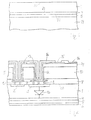
- Figure 1 shows a cross-section of a handling wafer 19 carrying an etch stop layer 5, a terminal layer 4 and a base layer 1, which has a front surface 20 and a rear surface 21 forming the boundary face to the terminal layer 4.
- the rear surface 22 of the terminal layer 4 is the boundary face to the etch stop layer 5.
- the front surface 20 is provided for the electric terminals and the wiring of the photodiode device.
- the handling wafer 19 may be silicon, for instance.
- the etch stop layer 5 may be produced by an epitaxial growth on the surface of the handling wafer 19.
- the terminal layer 4 is provided with high doping concentration as an anode or cathode layer of the photodiode.
- the base layer 1 may be intrinsically conducting semiconductor material, especially silicon, of either type of conductivity, rendering the structure of a PIN photodiode, or it may comprise a low doping for a high resistivity.
- the base layer 1 may be grown by epitaxy on the terminal layer 4.
- Figure 2 shows a cross-section according to Figure 1 after a further processing of the device.
- a first contact region 2 and a second contact region 3 are formed as doped regions of opposite types of conductivity and provided as terminals of the photodiode, which is schematically represented by the circuit symbol 18.
- a substrate 10 which may be a semiconductor material
- an intermediate layer 7 which may be an oxide of the semiconductor material.
- Contact plugs 8 connected to portions of a structured contact layer 9, which may be a metal, are arranged in the intermediate layer 7 on the first and second contact regions 2, 3, respectively.
- the first contact region 2 is provided with a first substrate via 11, and the second contact region 3 is provided with a second substrate via 12.
- the vias 11, 12 can be formed by a metalization 13, which may be separated from the substrate 10 by a dielectric layer 14.
- the contact plugs 8 and the vias 11, 12 are provided as electric terminal connections of the photodiode and are only an example, which may be substituted with electric connections or wirings of the photodiode that differ from the device structure shown in Figure 2 .
- the metalization 13 can be covered with a passivation layer 16, which may comprise contact windows 15 for an external electric contact.
- the handling wafer 19 is removed up to the etch stop layer 5.
- the handling wafer is a semiconductor material like silicon, it can be removed by grinding and a posterior wet etching that stops on the etch stop layer 5. The grinding process produces a rough surface, which is smoothed by the wet etching step.
- a high selectivity of the wet etching process is achieved with respect to the semiconductor material of the handling wafer 19.
- the etch stop layer may be a doped silicon layer, which has a sufficiently good etch selectivity versus intrinsically conducting silicon in alkaline solutions.
- Potassium hydroxide (KOH) or tetramethylammonium hydroxide (TMAH) can be used as the etching agent.
- the etch stop layer 5 may as well be SiGeC, which has a good selectivity versus silicon in wet etching processes. The selectivity depends on the C and Ge composition of the layer. Further to the mentioned alkaline solutions, HNA, which is a common isotropic etchant for silicon, can be used as the etching agent. Other possibilities of etch stop layers are an electrochemical etch stop and an etch stop that is effected at the transition from high to low doping concentrations in silicon.
- the rear side of the device which is intended for light incidence, may be coated, particularly with a passivation layer 6.
- a passivation layer 6 Its main purpose is a protection of the photodiode against an external attack of chemicals or adverse environmental conditions.
- the passivation layer 6 can also function as an antireflective coating.
- the passivation layer 6 may be a single layer or a layer sequence and may comprise, for instance, silicon oxide, silicon nitride, silicon oxidnitride or a combination of any of these, which can be deposited by a PECVD technique (plasma-enhanced chemical vapor deposition).
- PECVD technique plasma-enhanced chemical vapor deposition
- a dedicated antireflective coating may also be applied, in order to maximize the quantum efficiency for a given wavelength or a range of wavelengths, depending on the application.
- Embodiments according to Figures 1 and 2 may particularly comprise, apart from an intrisically conductive base layer 1 (p- or n- conductivity), the following combinations: etch stop layer 5 terminal layer 4 p+ n+ (cathode) n+ p+ (anode) SiGeC n+ (cathode) SiGeC p+ (anode)
- the doped layers can be produced with different dopants, like As for n-type and In or B for p-type conductivity, for instance.
- Figure 3 shows a cross-section according to Figure 1 for a further embodiment, in which the terminal layer 4 is used as the etch stop layer 5.
- the terminal layer 4 is highly doped for either conductivity type (p+ or n+ conductivity).
- the rear surface 22 of the terminal layer 4 is the boundary to the handling wafer 19.
- Figure 4 shows a cross-section according to Figure 2 for the embodiment according to Figure 3 .
- the dedicated etch stop layer 5 is substituted with the terminal layer 4, and a passivation layer 6 and/or an antireflective coating may be applied to the rear side, which is intended for light incidence.
- the other elements of this embodiment may be similar to the corresponding elements of the embodiment according to Figure 2 and are designated with the same reference numerals.
- the terminal layer 4 functions as anode (p+ conductivity) or cathode (n+ conductivity).
- Figure 5 shows a cross-section according to Figure 1 for a further embodiment, in which a pn junction is formed between the handling wafer 19 and the base layer 1.
- a depletion region 17 can be generated and used as the etch stop layer 5.
- the handling wafer 19 and the base layer 1 are provided with opposite types of conductivity.
- the handling wafer 19 may have p+ or p- conductivity if the base layer 1 has n- conductivity.
- the rear surface 21 of the base layer 1 is the boundary to the handling wafer 19; there the pn junction is located and the depletion region 17 is generated.
- Figure 6 shows a cross-section according to Figure 2 for the embodiment according to Figure 5 .
- the terminal layer 4 is formed by a residual layer portion of the handling wafer 19.
- the other elements of this embodiment may be similar to the corresponding elements of the embodiment according to Figure 2 and are designated with the same reference numerals.
- the handling wafer 19 is preferably highly doped, and the base layer 1 may be grown epitaxially as an intrinsically conductive silicon layer. After the integration of the photodiode the handling wafer 19 can be removed by using an electrochemical etch stop, which stops in the depletion region 17 of the pn junction when a bias is applied. This method is described in detail in the publication of R. L. Gealer et al. mentioned in the introduction.
- the described method of producing a photodiode device and the photodiode device comprising an etch stop layer offer new possibilities for fabricating three-dimensional integrated and backside illuminated photodiodes based on epitaxial processes, thereby substantially reducing the production costs, particularly when compared to conventional approaches using SOI materials.
Landscapes
- Light Receiving Elements (AREA)
Priority Applications (1)
| Application Number | Priority Date | Filing Date | Title |
|---|---|---|---|
| EP11176476A EP2555244A1 (fr) | 2011-08-03 | 2011-08-03 | Procédé de production d'un dispositif à photodiodes et dispositif à photodiodes comprenant une couche d'arrêt de gravure |
Applications Claiming Priority (1)
| Application Number | Priority Date | Filing Date | Title |
|---|---|---|---|
| EP11176476A EP2555244A1 (fr) | 2011-08-03 | 2011-08-03 | Procédé de production d'un dispositif à photodiodes et dispositif à photodiodes comprenant une couche d'arrêt de gravure |
Publications (1)
| Publication Number | Publication Date |
|---|---|
| EP2555244A1 true EP2555244A1 (fr) | 2013-02-06 |
Family
ID=44653995
Family Applications (1)
| Application Number | Title | Priority Date | Filing Date |
|---|---|---|---|
| EP11176476A Withdrawn EP2555244A1 (fr) | 2011-08-03 | 2011-08-03 | Procédé de production d'un dispositif à photodiodes et dispositif à photodiodes comprenant une couche d'arrêt de gravure |
Country Status (1)
| Country | Link |
|---|---|
| EP (1) | EP2555244A1 (fr) |
Citations (7)
| Publication number | Priority date | Publication date | Assignee | Title |
|---|---|---|---|---|
| US20040009649A1 (en) * | 2002-07-12 | 2004-01-15 | Kub Francis J. | Wafer bonding of thinned electronic materials and circuits to high performance substrates |
| US20060157811A1 (en) | 2000-04-20 | 2006-07-20 | Carlson Lars S | Fabrication of low leakage-current backside illuminated photodiodes |
| WO2007090055A1 (fr) * | 2006-01-31 | 2007-08-09 | Memc Electronic Materials, Inc. | Tranche a semi-conducteur a haute conductivite thermique |
| US20100148289A1 (en) * | 2008-12-17 | 2010-06-17 | Mccarten John P | Back illuminated sensor with low crosstalk |
| US20100193893A1 (en) | 2005-06-07 | 2010-08-05 | Gerald Meinhardt | Photodiode With Integrated Semiconductor Circuit and Method for the Production Thereof |
| US20100213565A1 (en) | 2006-06-05 | 2010-08-26 | Peter Steven Bui | High Speed Backside Illuminated, Front Side Contact Photodiode Array |
| WO2011013290A1 (fr) * | 2009-07-30 | 2011-02-03 | 信越半導体株式会社 | Procédé de fabrication dun dispositif à semi-conducteur |
-
2011
- 2011-08-03 EP EP11176476A patent/EP2555244A1/fr not_active Withdrawn
Patent Citations (7)
| Publication number | Priority date | Publication date | Assignee | Title |
|---|---|---|---|---|
| US20060157811A1 (en) | 2000-04-20 | 2006-07-20 | Carlson Lars S | Fabrication of low leakage-current backside illuminated photodiodes |
| US20040009649A1 (en) * | 2002-07-12 | 2004-01-15 | Kub Francis J. | Wafer bonding of thinned electronic materials and circuits to high performance substrates |
| US20100193893A1 (en) | 2005-06-07 | 2010-08-05 | Gerald Meinhardt | Photodiode With Integrated Semiconductor Circuit and Method for the Production Thereof |
| WO2007090055A1 (fr) * | 2006-01-31 | 2007-08-09 | Memc Electronic Materials, Inc. | Tranche a semi-conducteur a haute conductivite thermique |
| US20100213565A1 (en) | 2006-06-05 | 2010-08-26 | Peter Steven Bui | High Speed Backside Illuminated, Front Side Contact Photodiode Array |
| US20100148289A1 (en) * | 2008-12-17 | 2010-06-17 | Mccarten John P | Back illuminated sensor with low crosstalk |
| WO2011013290A1 (fr) * | 2009-07-30 | 2011-02-03 | 信越半導体株式会社 | Procédé de fabrication dun dispositif à semi-conducteur |
Non-Patent Citations (2)
| Title |
|---|
| R. L. GEALER, R. H. HAMMERLE, H. KARSTEN, H. S. WROBLOWA: "Electrochemical etch-stop control for silicon containing electronic components", J. APPL. ELECTROCHEMISTRY, vol. 18, 1988, pages 463 - 468 |
| R. L. GEALER, R. H. HAMMERLE, H. KARSTEN, H. S. WROBLOWA: "Electrochemical etch-stop control for silicon containing electronic components", J. APPL. ELECTROCHEMISTRY, vol. 18, 1988, pages 463 - 468, XP002665948 * |
Similar Documents
| Publication | Publication Date | Title |
|---|---|---|
| US10700222B2 (en) | Metallization of solar cells | |
| US6452086B1 (en) | Solar cell comprising a bypass diode | |
| CN107403799B (zh) | 半导体器件及其制造方法 | |
| US8115097B2 (en) | Grid-line-free contact for a photovoltaic cell | |
| US8368159B2 (en) | Photon counting UV-APD | |
| KR101655249B1 (ko) | 후방 접촉 슬리버 셀 | |
| US4847210A (en) | Integrated pin photo-detector method | |
| US7489014B2 (en) | Front side electrical contact for photodetector array and method of making same | |
| US4926231A (en) | Integrated pin photo-detector | |
| US10032942B2 (en) | Solar cell having Ti- or Ta-containing thermal and diffusion barrier layer for foil-based metallization | |
| KR20070099938A (ko) | 태양 전지 | |
| US8829332B1 (en) | Photovoltaic device formed on porous silicon isolation | |
| US9018726B2 (en) | Photodiode and production method | |
| US20140273332A1 (en) | Method for producing photovoltaic device isolated by porous silicon | |
| EP3226308B1 (fr) | Dispositif de rupture de tension pour cellules solaires | |
| EP2555244A1 (fr) | Procédé de production d'un dispositif à photodiodes et dispositif à photodiodes comprenant une couche d'arrêt de gravure | |
| CN218896638U (zh) | 集成光学传感器、成像系统以及电子设备 | |
| CN117116957A (zh) | 一种单光子雪崩二极管阵列及其制备方法 | |
| US12457823B2 (en) | Photodetector structure with air gap and related methods | |
| US9570637B2 (en) | Solar cell and manufacturing method of the same | |
| KR100971301B1 (ko) | 태양전지 및 그 제조방법 | |
| JPH0230189A (ja) | 半導体光検出装置 |
Legal Events
| Date | Code | Title | Description |
|---|---|---|---|
| PUAI | Public reference made under article 153(3) epc to a published international application that has entered the european phase |
Free format text: ORIGINAL CODE: 0009012 |
|
| AK | Designated contracting states |
Kind code of ref document: A1 Designated state(s): AL AT BE BG CH CY CZ DE DK EE ES FI FR GB GR HR HU IE IS IT LI LT LU LV MC MK MT NL NO PL PT RO RS SE SI SK SM TR |
|
| AX | Request for extension of the european patent |
Extension state: BA ME |
|
| STAA | Information on the status of an ep patent application or granted ep patent |
Free format text: STATUS: THE APPLICATION IS DEEMED TO BE WITHDRAWN |
|
| 18D | Application deemed to be withdrawn |
Effective date: 20130807 |