EP2555256A2 - Halbleiter-template-substrat, lichtemittierendes element mit einem halbleiter-template-substrat und herstellungsverfahren dafür - Google Patents
Halbleiter-template-substrat, lichtemittierendes element mit einem halbleiter-template-substrat und herstellungsverfahren dafür Download PDFInfo
- Publication number
- EP2555256A2 EP2555256A2 EP11763054A EP11763054A EP2555256A2 EP 2555256 A2 EP2555256 A2 EP 2555256A2 EP 11763054 A EP11763054 A EP 11763054A EP 11763054 A EP11763054 A EP 11763054A EP 2555256 A2 EP2555256 A2 EP 2555256A2
- Authority
- EP
- European Patent Office
- Prior art keywords
- light
- buffer layer
- emitting device
- semiconductor layer
- pyramid structures
- Prior art date
- Legal status (The legal status is an assumption and is not a legal conclusion. Google has not performed a legal analysis and makes no representation as to the accuracy of the status listed.)
- Withdrawn
Links
Images






Classifications
-
- H—ELECTRICITY
- H10—SEMICONDUCTOR DEVICES; ELECTRIC SOLID-STATE DEVICES NOT OTHERWISE PROVIDED FOR
- H10H—INORGANIC LIGHT-EMITTING SEMICONDUCTOR DEVICES HAVING POTENTIAL BARRIERS
- H10H20/00—Individual inorganic light-emitting semiconductor devices having potential barriers, e.g. light-emitting diodes [LED]
- H10H20/01—Manufacture or treatment
- H10H20/011—Manufacture or treatment of bodies, e.g. forming semiconductor layers
- H10H20/018—Bonding of wafers
-
- H—ELECTRICITY
- H10—SEMICONDUCTOR DEVICES; ELECTRIC SOLID-STATE DEVICES NOT OTHERWISE PROVIDED FOR
- H10H—INORGANIC LIGHT-EMITTING SEMICONDUCTOR DEVICES HAVING POTENTIAL BARRIERS
- H10H20/00—Individual inorganic light-emitting semiconductor devices having potential barriers, e.g. light-emitting diodes [LED]
- H10H20/01—Manufacture or treatment
- H10H20/011—Manufacture or treatment of bodies, e.g. forming semiconductor layers
- H10H20/013—Manufacture or treatment of bodies, e.g. forming semiconductor layers having light-emitting regions comprising only Group III-V materials
- H10H20/0133—Manufacture or treatment of bodies, e.g. forming semiconductor layers having light-emitting regions comprising only Group III-V materials with a substrate not being Group III-V materials
- H10H20/01335—Manufacture or treatment of bodies, e.g. forming semiconductor layers having light-emitting regions comprising only Group III-V materials with a substrate not being Group III-V materials the light-emitting regions comprising nitride materials
-
- H—ELECTRICITY
- H10—SEMICONDUCTOR DEVICES; ELECTRIC SOLID-STATE DEVICES NOT OTHERWISE PROVIDED FOR
- H10H—INORGANIC LIGHT-EMITTING SEMICONDUCTOR DEVICES HAVING POTENTIAL BARRIERS
- H10H20/00—Individual inorganic light-emitting semiconductor devices having potential barriers, e.g. light-emitting diodes [LED]
- H10H20/80—Constructional details
- H10H20/81—Bodies
- H10H20/815—Bodies having stress relaxation structures, e.g. buffer layers
-
- H—ELECTRICITY
- H10—SEMICONDUCTOR DEVICES; ELECTRIC SOLID-STATE DEVICES NOT OTHERWISE PROVIDED FOR
- H10P—GENERIC PROCESSES OR APPARATUS FOR THE MANUFACTURE OR TREATMENT OF DEVICES COVERED BY CLASS H10
- H10P14/00—Formation of materials, e.g. in the shape of layers or pillars
- H10P14/20—Formation of materials, e.g. in the shape of layers or pillars of semiconductor materials
- H10P14/27—Formation of materials, e.g. in the shape of layers or pillars of semiconductor materials using selective deposition, e.g. simultaneous growth of monocrystalline and non-monocrystalline semiconductor materials
- H10P14/271—Formation of materials, e.g. in the shape of layers or pillars of semiconductor materials using selective deposition, e.g. simultaneous growth of monocrystalline and non-monocrystalline semiconductor materials characterised by the preparation of substrate for selective deposition
- H10P14/272—Formation of materials, e.g. in the shape of layers or pillars of semiconductor materials using selective deposition, e.g. simultaneous growth of monocrystalline and non-monocrystalline semiconductor materials characterised by the preparation of substrate for selective deposition using mask materials other than SiO2 or SiN
-
- H—ELECTRICITY
- H10—SEMICONDUCTOR DEVICES; ELECTRIC SOLID-STATE DEVICES NOT OTHERWISE PROVIDED FOR
- H10P—GENERIC PROCESSES OR APPARATUS FOR THE MANUFACTURE OR TREATMENT OF DEVICES COVERED BY CLASS H10
- H10P14/00—Formation of materials, e.g. in the shape of layers or pillars
- H10P14/20—Formation of materials, e.g. in the shape of layers or pillars of semiconductor materials
- H10P14/27—Formation of materials, e.g. in the shape of layers or pillars of semiconductor materials using selective deposition, e.g. simultaneous growth of monocrystalline and non-monocrystalline semiconductor materials
- H10P14/276—Lateral overgrowth
- H10P14/278—Pendeoepitaxy
-
- H—ELECTRICITY
- H10—SEMICONDUCTOR DEVICES; ELECTRIC SOLID-STATE DEVICES NOT OTHERWISE PROVIDED FOR
- H10P—GENERIC PROCESSES OR APPARATUS FOR THE MANUFACTURE OR TREATMENT OF DEVICES COVERED BY CLASS H10
- H10P14/00—Formation of materials, e.g. in the shape of layers or pillars
- H10P14/20—Formation of materials, e.g. in the shape of layers or pillars of semiconductor materials
- H10P14/29—Formation of materials, e.g. in the shape of layers or pillars of semiconductor materials characterised by the substrates
- H10P14/2901—Materials
-
- H—ELECTRICITY
- H10—SEMICONDUCTOR DEVICES; ELECTRIC SOLID-STATE DEVICES NOT OTHERWISE PROVIDED FOR
- H10P—GENERIC PROCESSES OR APPARATUS FOR THE MANUFACTURE OR TREATMENT OF DEVICES COVERED BY CLASS H10
- H10P14/00—Formation of materials, e.g. in the shape of layers or pillars
- H10P14/20—Formation of materials, e.g. in the shape of layers or pillars of semiconductor materials
- H10P14/29—Formation of materials, e.g. in the shape of layers or pillars of semiconductor materials characterised by the substrates
- H10P14/2901—Materials
- H10P14/2921—Materials being crystalline insulating materials
-
- H—ELECTRICITY
- H10—SEMICONDUCTOR DEVICES; ELECTRIC SOLID-STATE DEVICES NOT OTHERWISE PROVIDED FOR
- H10P—GENERIC PROCESSES OR APPARATUS FOR THE MANUFACTURE OR TREATMENT OF DEVICES COVERED BY CLASS H10
- H10P14/00—Formation of materials, e.g. in the shape of layers or pillars
- H10P14/20—Formation of materials, e.g. in the shape of layers or pillars of semiconductor materials
- H10P14/32—Formation of materials, e.g. in the shape of layers or pillars of semiconductor materials characterised by intermediate layers between substrates and deposited layers
- H10P14/3202—Materials thereof
-
- H—ELECTRICITY
- H10—SEMICONDUCTOR DEVICES; ELECTRIC SOLID-STATE DEVICES NOT OTHERWISE PROVIDED FOR
- H10P—GENERIC PROCESSES OR APPARATUS FOR THE MANUFACTURE OR TREATMENT OF DEVICES COVERED BY CLASS H10
- H10P14/00—Formation of materials, e.g. in the shape of layers or pillars
- H10P14/20—Formation of materials, e.g. in the shape of layers or pillars of semiconductor materials
- H10P14/32—Formation of materials, e.g. in the shape of layers or pillars of semiconductor materials characterised by intermediate layers between substrates and deposited layers
- H10P14/3202—Materials thereof
- H10P14/3214—Materials thereof being Group IIIA-VA semiconductors
- H10P14/3216—Nitrides
-
- H—ELECTRICITY
- H10—SEMICONDUCTOR DEVICES; ELECTRIC SOLID-STATE DEVICES NOT OTHERWISE PROVIDED FOR
- H10P—GENERIC PROCESSES OR APPARATUS FOR THE MANUFACTURE OR TREATMENT OF DEVICES COVERED BY CLASS H10
- H10P14/00—Formation of materials, e.g. in the shape of layers or pillars
- H10P14/20—Formation of materials, e.g. in the shape of layers or pillars of semiconductor materials
- H10P14/34—Deposited materials, e.g. layers
- H10P14/3402—Deposited materials, e.g. layers characterised by the chemical composition
- H10P14/3414—Deposited materials, e.g. layers characterised by the chemical composition being group IIIA-VIA materials
- H10P14/3416—Nitrides
-
- H—ELECTRICITY
- H10—SEMICONDUCTOR DEVICES; ELECTRIC SOLID-STATE DEVICES NOT OTHERWISE PROVIDED FOR
- H10P—GENERIC PROCESSES OR APPARATUS FOR THE MANUFACTURE OR TREATMENT OF DEVICES COVERED BY CLASS H10
- H10P14/00—Formation of materials, e.g. in the shape of layers or pillars
- H10P14/20—Formation of materials, e.g. in the shape of layers or pillars of semiconductor materials
- H10P14/38—Formation of materials, e.g. in the shape of layers or pillars of semiconductor materials characterised by treatments done after the formation of the materials
Definitions
- the present invention relates to a semiconductor template substrate, a light-emitting device using the same, and a method of manufacturing the light-emitting device, and more particularly, to a semiconductor template substrate for decreasing defective crystalline and enabling easy separation, a light-emitting device using the same, and a method of manufacturing the light-emitting device.
- Fig. 6A illustrates a conventional horizontal semiconductor light-emitting device
- Fig. 6B illustrates a conventional vertical semiconductor light-emitting device.
- the horizontal semiconductor light-emitting device includes a buffer layer 2, an n-type nitride semiconductor layer 3, an active layer 4, and a p-type nitride semiconductor layer 5 that are sequentially stacked on a sapphire substrate 1.
- a p-type electrode 6 is formed on the p-type nitride semiconductor layer 5, and, by removing a partial region of the p-type nitride semiconductor layer 5 and active layer 4 in an etching process, an n-type electrode 7 is formed on an exposed portion of the n-type nitride semiconductor layer 3.
- a light-emitting area is relatively reduced, and a surface leakage current increases, causing the decrease in the emission performance of the horizontal light-emitting device.
- a resistance increases, and thus, an operating voltage increases. For this reason, heat is generated, causing the reduction in the service life of the horizontal light-emitting device.
- an operation of forming a p-type nitride semiconductor layer 5 on a substrate is the same as that of the horizontal light-emitting device.
- An insulating substrate is separated from the light-emitting device before an n-type electrode 7 is formed, and then, the n-type electrode 7 is formed at a bottom of an n-type semiconductor layer 3.
- a laser lift-off process is generally used for separation of the insulating substrate.
- the laser beam By irradiating a laser beam, which is a strong energy source, on a backside of a transparent sapphire substrate, the laser beam is strongly absorbed in a interface between a buffer layer and the sapphire substrate, and thus, a temperature of 900 °C or more is momentarily produced, whereby a nitride semiconductor in the interface is thermo-chemically dissolved and the sapphire substrate is separated from the vertical light-emitting device.
- the laser lift-off process causes the thermal/mechanical deformation of a light-emitting stack structure including an active layer.
- a mechanical stress occurs between the nitride semiconductor layer and a thick sapphire substrate due to different lattice constants and heat expansion coefficients, and, the vertical nitride semiconductor light-emitting device suffers a mechanical/thermal damage because the vertical nitride semiconductor light-emitting device cannot endure the mechanical stress.
- the present invention provides a semiconductor template substrate for preventing the damage of a semiconductor substrate in performing a separation process.
- the present invention provides an excellent semiconductor light-emitting device.
- the present invention provides a method of manufacturing an excellent semiconductor light-emitting device.
- the present invention relates to an approach to solve the above described problems.
- a separation layer is used to facilitate ease separation of the light-emitting device from a semiconductor substrate.
- the light-emitting device has an inverted pyramid structure due to the separation layer.
- a light-emitting device in accordance with a first aspect of the present invention, there is provided a light-emitting device.
- the light-emitting includes a semiconductor layer, a light-emitting stack structure, and a plurality of inverted pyramid structures.
- the light-emitting stack structure is formed on a first surface of the semiconductor layer and each of the inverted pyramid structures is formed on a second surface of the semiconductor layer opposite to the first surface.
- Each of the inverted pyramid structures has a sectional area decreasing as each of the inverted pyramid structures is more extended in a vertical direction from the second surface.
- a method of manufacturing a light-emitting device A buffer layer is formed on a substrate. A plurality of pyramid structures protruding from the buffer layer. A semiconductor layer separated from the buffer layer is formed. A semiconductor layer separated from the buffer layer is formed by growing a crystal from on each of the pyramid structures. The pyramid structures connect the buffer layer and the semiconductor layer. A light-emitting stack structure is formed on the semiconductor layer. Each of the pyramid structures is severed or a contact surface between each of the pyramid structures and the buffer layer is separated to separate the semiconductor layer from the buffer layer.
- a buffer layer is formed on a substrate.
- the buffer layer is divided into a plurality of separate light-emitting device regions to form divided separate semiconductor layers respectively formed in the separate light-emitting device regions.
- the separate semiconductor layers respectively formed in the separate light-emitting device regions are connected to the buffer layer corresponding to the separate light-emitting device regions by a plurality of protrusions.
- a light-emitting stack structure is formed on each of the separate semiconductor layers.
- Each of the pyramid structures is severed or a contact surface between each of the pyramid structures and the buffer layer is separated to separate the semiconductor layers from the buffer layer.
- a buffer layer is formed on a substrate.
- the buffer layer is divided into a plurality of light-emitting device regions, and a plurality of pyramid structures are respectively formed in the light-emitting device regions.
- the pyramid structures is grown from respective tops of the pyramid structures to form a semiconductor layer having a cleavage surface that divides the light-emitting device regions.
- the semiconductor layer and the buffer layer are connected by the pyramid structures, and the semiconductor layer is separated from the buffer lay.
- a light-emitting stack structure is formed on the semiconductor layer to make a separate auxiliary light-emitting device.
- Each of the pyramid structures to strip the semiconductor layer is severed from the buffer layer.
- the separate auxiliary light-emitting device is separated with respect to the cleavage surface.
- a buffer layer is formed on a substrate.
- the buffer layer is divided into a plurality of light-emitting device regions to form a plurality of pyramid structures in the light-emitting device regions.
- the pyramid structures is grown from respective tops of the pyramid structures to form a plurality of semiconductor layers that correspond to the respective light-emitting device regions and are separated from each other are formed.
- the semiconductor layers and the buffer layer are connected by the pyramid structures, and the semiconductor layers are separated from the buffer layer.
- the light-emitting stack structures are formed on the semiconductor layers to form separate light-emitting devices.
- the pyramid structures is severed to form light-emitting devices separated each other.
- a semiconductor substrate template in accordance with a sixth aspect of the present invention, there is provided a semiconductor substrate template.
- the semiconductor substrate template includes a buffer layer formed on a substrate, a plurality of pyramid structures formed on the buffer layer, and a semiconductor layer formed on the buffer layer.
- the semiconductor layer is separated from the buffer layer and connected to the buffer layer by the plurality of pyramid structures.
- a semiconductor substrate template in accordance with a seventh aspect of the present invention, there is provided a semiconductor substrate template.
- the semiconductor substrate template includes a buffer layer formed on a substrate, the buffer layer being divided into a plurality of auxiliary light-emitting regions, a plurality of protrusions protruding upward from the respective auxiliary light-emitting regions, and a plurality of separate semiconductor layers formed on the respective protrusions to be separated from the buffer layer, in the respective auxiliary light-emitting regions.
- a semiconductor substrate is simply separated from an insulating substrate, and thus, the semiconductor substrate is not damaged, thereby manufacturing a light-emitting device having excellent performance.
- a concave-convex pattern is formed at a bottom of a semiconductor substrate without a separate additional process, thus simplifying a manufacturing process.
- the semiconductor substrate cannot be damaged even in a process of separating a separate light-emitting device from the semiconductor substrate.
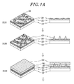
- Figs. 1A and 1B are views illustrating a method of manufacturing a light-emitting device in accordance with an embodiment of the present invention
- Figs. 2A and 2B are views for describing a method of manufacturing a light-emitting device in accordance with another embodiment of the present invention.
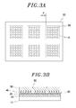
- Figs. 3A to 3G are views for describing a method of manufacturing a light-emitting device in accordance with another embodiment of the present invention.
- Fig. 4 is a view schematically illustrating a jig for forming an electrode
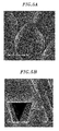
- Figs. 5A to 5C are views illustrating in-process materials of a light-emitting device manufactured in accordance with an embodiment of the present invention.
- Figs. 6A and 6B are views schematically illustrating a conventional horizontal light-emitting device and a conventional vertical light-emitting device.
- the present embodiment is an embodiment for growing an n-type GaN crystal with a sapphire substrate.
- materials that are used for a substrate and a buffer layer, a semiconductor layer, and a light-emitting stack structure are not limited thereto.
- a buffer layer 20 is formed on an insulating substrate 10, and a mask layer 30 having a plurality of exposure patterns 39 is formed on the buffer layer 20.
- the exposure patterns 39 are illustrated in a circular shape. However, the exposure patterns 39 may be formed in a polygonal shape such as a tetragonal shape, a triangular shape, or a hexagonal shape, and may be variously arranged.
- the substrate 10 may be a sapphire substrate or a substrate including silicon, GaAs, InP, and SiC, and may be selected from a group consisting of various materials.
- the buffer layer 20 may be formed by growing a GaN crystal.
- the buffer layer 20 may be formed by growing an n-type GaN crystal to a thickness of 2 ⁇ m to 5 ⁇ m with a HVPE crystal growing device.
- the buffer layer 20 may include an AlxGa(1-x)N (0 ⁇ x ⁇ 1) layer or Al 2 O 3 , and AlN or ZnO.
- the material of the mask layer 30 may use SiO 2 or Si 3 N 4 , and metal such as Cr, Au, Ti, or Ni.
- SiO 2 or Si 3 N 4 is deposited to a thickness of 500 ⁇ to 5000 ⁇ on the buffer layer 20 in PECVD, and then, by forming the exposure pattern 39 in a photolithography process, a portion of the buffer layer 20 is exposed.
- the exposure pattern may be formed by depositing SiO 2 or Si 3 N 4 to a thickness of 500 ⁇ to 5000 ⁇ , or metal such as Cr, Au, Ti, or Ni may be deposited in an exposure pattern shape.
- the mask layer 30 may be formed by a lift-off process. Photoresist is applied on the buffer layer 20, and an exposure process is performed. Subsequently, a photoresist pattern is formed by performing a development process. Therefore, the buffer layer 20 having a desired pattern shape is exposed, and the other portion is covered by the photoresist pattern. An auxiliary mask layer (not shown) is formed on the photoresist pattern formed on the buffer layer 20. Subsequently, the photoresist pattern and the auxiliary mask layer formed on the photoresist pattern are removed. Accordingly, the mask layer 30 having a desired pattern may be formed on the buffer layer 20.
- a diameter of each of the exposure patterns 39 is about 0.5 ⁇ m to about 5 ⁇ m, and an interval between adjacent exposure patterns 39 is about 05. ⁇ m to about 10 ⁇ m.
- a crystal is grown from the buffer layer 20 exposed by the exposure pattern 39.
- a pyramid structure 40 is formed from the inside of the exposure pattern 39 of the mask layer 30. This denotes that a sectional area of the pyramid structure 40 becomes narrower progressively closer to an upper portion of the pyramid structure 40.
- the pyramid structure 40 may have a conic structure or a hexagonal pyramid (polygonal pyramid) structure.
- a basic crystalline structure of GaN is a wurtzite structure, and thus, by growing GaN from the buffer layer 20 (exposed by the exposure pattern 39) to have a homed shape, a hexagonal pyramid structure may be formed.
- a diameter of a bottom of the pyramid structure 40 may be approximately equal to or slightly greater than that of the exposure pattern 39.
- a height of the pyramid structure 40 may be about 0.5 ⁇ m to about 7.5 ⁇ m greater by about 1 to 5 times than the diameter of the exposure pattern 39.
- the bottom of the pyramid structure 40 is overgrown, and thus becomes broader than the exposure pattern 39.
- the pyramid structure 40 protrudes to on the mask layer 30.
- the pyramid structure 40 may be formed in a hexagonal pyramid structure.
- an example of a crystal growth condition of HVPE is as follows. Ga metal is used as a raw material of Ga, NH 3 is used as a raw material of N, and Te or Si is mixed with Ga solution for forming n-type GaN.
- the substrate with the exposure pattern 39 formed therein is disposed in a reaction pipe, and, by growing a GaN crystal at about 1000 °C to 1100 °C, a hexagonal pyramid structure of n-type GaN is formed.
- a composition of the pyramid structure 40 may be AlxGa(1-x)N (0 ⁇ x ⁇ 1).
- a composition of the buffer layer 30 and the composition of the pyramid structure 40 may be formed identically or differently.
- AlxGa(1-x)N (0 ⁇ x ⁇ 1) layer that is the buffer layer 20 by adjusting the amount of Al (which is added into Ga solution that is used in forming the buffer layer 20) from 0 g to several g to hundreds mg per 1 g Ga, GaN whose a composition x is 0 to AlN whose a composition x is 1 may be obtained.
- an AlxGa(1-x)N (0 ⁇ x ⁇ 1) layer that is the buffer layer 20 by adjusting the amount of Al (which is added into Ga solution that is used in forming the pyramid structure 40) from 0 g to several mg to hundreds mg perr 1g Ga, GaN (whose a composition x is 0) to AlN whose a composition x is 1 may be obtained.
- the composition of the buffer layer 20 and the composition of the pyramid structure 40 are adjusted by changing a source. That is, the composition of the buffer layer 30 and the composition of the pyramid structure 40 may be formed identically or differently.
- Fig. 5A is an SEM photograph in a state in which the pyramid structure 40 has been formed in accordance with an embodiment of the present invention.
- the pyramid structure 40 is formed, and a semiconductor layer 50 is then formed in operation S130.
- the semiconductor layer 50 may be formed with the HVPE crystal growing device. For example, growth layers grown from respective side surfaces of the pyramid structures 40 may be coupled, thereby forming the semiconductor layer 50. That is, in the mask layer 30, it is difficult for a crystal to grow from the buffer layer 20. A GaN crystal starts to grow to an inclined side surface of the exposed pyramid structure 40, and crystal layers grown from the semiconductor layer 50 adjacent thereto are adhered to each other, thereby forming the semiconductor layer 50.
- a height of the semiconductor layer 50 may be a thickness that enables the pyramid structure 40 to sustain the thickness of the semiconductor layer 50.
- the height of the semiconductor layer 50 may be about 1 ⁇ m to 100 ⁇ m.
- the composition of the pyramid structure 40 may be GaN or AlxGa(1-x)N (0 ⁇ x ⁇ 1).
- a source growing the pyramid structure 40 differs from a source growing the semiconductor layer 50
- layers having different compositions may be obtained.
- Ga source reacts with ammonia for forming the pyramid structure 40
- Ga source reacts with Al source and ammonia for forming the semiconductor layer 50.
- the pyramid structure 40 is formed of GaN
- the semiconductor layer 50 is formed of AlGaN.
- an Al composition of the AlGaN layer may be adjusted.
- the composition of the pyramid structure 40 is merely one example, and, by changing a source used to form the pyramid structure 40, the pyramid structure 40 having another composition may be formed.
- a top of the semiconductor layer 50 may be a flat planarization layer.
- a crystal may start to grow from approximate half of the height of the pyramid structure 40 to the inclined side surface of the pyramid structure 40, crystals grown from adjacent pyramid structures 40 may be adhered to each other, and then, while maintaining growth until an entire region is planarized, the semiconductor layer 50 may be formed.
- the bottom of the semiconductor layer 50 may be formed at a position corresponding to one-third of the height of the pyramid structure 40.
- the technical spirit and scope of the present invention are not limited to the height.
- An empty space surrounded by the semiconductor layer 50, pyramid structure 40, and mask layer 30 is formed.
- a separation layer 90 is formed between the bottom of the semiconductor layer 50 and the mask layer 30.
- Fig. 5B is a side SEM photograph in a state in which the pyramid structure 40 and the semiconductor layer 50 have been formed in accordance with an embodiment of the present invention, and an empty space next to the pyramid structure can be seen.
- a light-emitting stack structure 60 is formed on the semiconductor layer 50.
- the light-emitting stack structure may be formed by forming an n-type AlGaN cladding layer, an AlGaN active layer, a p-type AlGaN cladding layer, and a p-type GaN cap layer.
- the light-emitting stack structure 60 may be formed by a HVPE crystal growing process.
- a cladding layer including n-type AlxGa(1-x)N (0 ⁇ x ⁇ 1), an active layer including AlxGa(1-x)N (0 ⁇ x ⁇ 1), a cladding layer including p-type AlxGa(1-x)N (0 ⁇ x ⁇ 1), and a p-type GaN cap layer may be sequentially formed.
- Materials of the respective layers of the light-emitting stack structure 60 and a stack sequence may be appropriately changed depending on an emission wavelength range, a light output, or the kind of a light-emitting device.
- the buffer layer 20, the semiconductor layer 50, and the light-emitting stack structure 60 may all be formed by the HVPE process, and thus, the buffer layer 20, the semiconductor layer 50, and the light-emitting stack structure 60 may be formed sequentially.
- the buffer layer 20, the semiconductor layer 50, and the light-emitting stack structure 60 may all be formed by an in-situ process.
- the substrate 10, the buffer layer 20, and the mask layer 30 are separated from the light-emitting stack structure 60. Unevenness may be formed on a separated surface.
- the separation of the substrate 10 may be performed by applying ultrasonic waves, physical vibration, or an impact.
- the pyramid structure 40 is severed from the separation layer 90 in which the semiconductor layer 50 and the buffer layer 40 are connected to only the pyramid structure 40, whereby separation is made.
- the pyramid structure 40 may be severed by applying a simple impact.
- an inverted pyramid structure is formed at the bottom of the semiconductor layer 50.
- the inverted pyramid structure denotes a structure in which a cross-sectional area increases progressively farther away from the bottom of the semiconductor layer 50. That is, the inverted pyramid structure formed at the semiconductor layer 50 serves as a structure that facilitates separation between the light-emitting device and the substrate 10 used to form the light-emitting device.
- separation is performed by irradiating a laser beam, separation is performed by irradiating the laser beam on the pyramid structure 40 of the separation layer 90 having relatively weak coupling strength compared to a conventional laser lift-off process, and thus, only a narrow region of a pyramid lower portion is thermally and chemically damaged by the laser beam, whereby the substrate 10 is separated from the light-emitting device without damaging the light-emitting stack structure 60.
- stress occurs in the pyramid structure 40 by applying strain to the substrate 10 and/or the buffer layer 20, thereby severing the pyramid structure 40.
- the separation layer 90 Due to the separation layer 90, the light-emitting device is easily separated from the substrate 10, and thus, a complicated process is not performed. Also, when separating the light-emitting device from the substrate 10, the semiconductor layer 50 of the light-emitting device is not damaged, and thus, a good-quality light-emitting device can be manufactured.
- Fig. 5C is an SEM photograph showing the bottom of the separated light-emitting stack structure, and a concave-convex pattern formed in severing the pyramid structure 40 can be seen.
- a p-type electrode 71 is formed on the light-emitting stack structure 60, and an n-type electrode 72 is formed at a bottom 51 of the separated semiconductor layer 50, thereby forming the light-emitting device.
- the n-type electrode 72 may be formed on the inverted pyramid structure, or formed at the bottom 51 of the semiconductor layer 50. Also, a separate intermediate layer may be formed, and then the electrodes 71 and 72 may be completely formed, depending on its design. In this case, in the bottom 51 of the semiconductor layer 50, the inverted pyramid structure may be formed by severing the pyramid structure 40. Also, since the bottom of the pyramid structure 40 is separated from the substrate 10, a protrusion pattern may be formed at the bottom 51 of the semiconductor layer 50 even without a separate pattern process.
- the p-type electrode 71 may be formed immediately before separation operation S510 after operation S140 of forming the light-emitting stack structure 60.
- the substrate 10 which has a structure before a process of separating the substrate 10 and on which the elements from the buffer layer 20 to the semiconductor layer 50 are formed through operation S140, may be used as a semiconductor template substrate.
- various electronic device structures are formed on the semiconductor template substrate, and then, by separating the separation layer 90, various vertical semiconductor devices may be manufactured.
- a second embodiment is substantially similar to a first embodiment, but relates to a method in which a region of the separation layer 90 is divided into a plurality of regions having different coupling strengths, and a light-emitting device is formed. Therefore, in forming the mask layer 30, as illustrated in Fig. 2A , the region of the separation layer 90 is divided into a first region 31 having relatively high coupling strength and a second region 32 having relatively low coupling strength.
- a diameter of each exposure pattern in the first region 31 differs from that of each exposure pattern in the second region 32, and an interval between the exposure patterns in the first region 31 differs from an interval between the exposure patterns in the second region 32.
- the diameter of each exposure pattern in the first region 31 having relatively high coupling strength is less than that of each exposure pattern in the second region 32 having relatively low coupling strength
- the interval between the exposure patterns in the first region 31 is less than the interval between the exposure patterns in the second region 32.
- the diameter of each exposure pattern and the interval between the exposure patterns in the first region 31 may be 1 ⁇ m
- the diameter of each exposure pattern and the interval between the exposure patterns in the second region 32 may be 3 ⁇ m.
- the pyramid structure 40 formed in the first region 31 has a gradient higher than the pyramid structure 40 formed in the second region 32.
- hexagonal pyramids are closely adhered to each other, and thus, an empty space is relatively reduced. Therefore, the separation layer 90 formed between the mask layer 30 and the semiconductor layer 50 is divided into a first separation part 91 having relatively high coupling strength and a second separation part 92 having relatively low coupling strength.
- the second embodiment is useful for a case in which the p-type electrode 71 is first formed before the separation layer 90 is separated.
- a method of manufacturing a light-emitting device in accordance with another embodiment of the present invention will be described with reference to Figs. 3A to 3D .
- a method of manufacturing one light-emitting device has been described.
- the present embodiment relates a method of manufacturing light-emitting devices in which a plurality of light-emitting devices are formed on one substrate and easily separated from the one substrate, and moreover, the light-emitting devices are easily separated from each other. Therefore, a manufacturing method similar to Fig. 1 will not be described.
- a buffer layer 20 is formed on a substrate 10, and a mask layer 30 that is as illustrated in Fig. 3A is formed on the buffer layer 20.
- the mask layer 30 has a plurality of light-emitting chip regions 'A'.
- each of the light-emitting chip regions 'A' is illustrated in a tetragonal shape.
- the light-emitting chip area 'A' is not limited to a tetragonal shape, and may be formed in various shapes such as a circular shape and a hexagonal shape depending on its design.
- the light-emitting chip regions 'A' are separated from each other by a certain chip interval 'd'.
- a plurality of exposure patterns 39 are formed in each light-emitting chip region of the mask layer 30.
- the mask layer 30 is formed, and then, as illustrated in Fig. 3B , a plurality of pyramid structures 40 are formed by selectively growing a crystal from the buffer layer 20 in the HVPE process, whereupon a semiconductor layer 50 is formed.
- a cleavage surface 55 that divides the semiconductor layer 50 into a plurality of separate light-emitting stack structures may be formed.
- a depth of the cleavage surface 55 may be adjusted to a depth a user desires, depending on a chip interval 'd' and a process condition.
- the depth of the cleavage surface 55 may be adjusted by adjusting a ratio of the height 'h' and the chip interval 'd'. For example, by adjusting the chip interval 'd' to less by about 0.4 to 0.6 times than the height 'h', as illustrated in Fig. 3C , a structure may be formed in which only a portion of the semiconductor chip 50 is connected and the light-emitting stack structures 60 are separated from each other.
- the light-emitting stack structure is formed on the semiconductor layer 50.
- the light-emitting stack structure 60 is divided into a plurality of light-emitting chip regions by the cleavage surface 51 of the semiconductor layer 50 for the formation thereof.
- each of the light-emitting devices is separated in vertical and horizontal directions.
- Such a separation process may be performed in different sequences.
- the substrate 10 is first separated in the vertical direction, and each of the light-emitting devices is then be separated in the horizontal direction. Separation in the horizontal direction may be performed by various processes using a physical impact or pressurization. For example, a film is adhered onto the light-emitting devices, and then, by compressing the film with a roller, each of the light-emitting devices may be separated. Alternatively, by applying appropriate vibration or pressure, separation in the horizontal direction and separation in the vertical direction may be performed simultaneously.
- a p-type electrode (not shown) is formed on the light-emitting stack structure 60, and an n-type electrode (not shown) is formed at a bottom of the separated semiconductor layer 50, thereby finishing the light-emitting device.
- a separate intermediate layer may be formed and each of the electrodes is then completely formed.
- the p-type electrode (not shown) may be formed at an appropriate time before or after a vertical separation operation and after a horizontal separation operation.
- the n-type electrode (not shown) may be formed before or after the horizontal separation operation.
- a jig 200 for forming an electrode may be used.
- the jig 200 includes a matrix type of chip containers 210 having an appropriate size for accommodating a plurality of light-emitting chips 100.
- a chip selector selects a chip 100 and puts the selected chip 100 into each of chip containers 210 included in the jig 200, and then, the electrodes are formed.
- the mask layer 30 is formed, and then, by selectively growing a crystal from the buffer layer 20, the plurality of pyramid structures are formed, whereupon the semiconductor layer 50 is formed.
- the semiconductor layer 50 may be separated and formed in units of separate light-emitting device. For example, by adjusting the chip interval d to greater by 0.4 to 0.6 times than the height h, the separately separated semiconductor layers 50 and the separate light-emitting stack structures 60 may be formed.
- the light-emitting stack structure 60 may be formed on each of the semiconductor layers 50, and, as illustrated in Fig.
- the semiconductor layers 50 may be separated from the buffer layer 30, thereby obtaining the separate light-emitting stack structures 60. Subsequently, the p-type electrode (not shown) is formed on each of the light-emitting stack structures 60, and the n-type electrode (not shown) is formed at a bottom of each of the separated semiconductor layers 50, thereby finishing the plurality of light-emitting devices.
- a semiconductor layer is formed on a pyramid structure, and then, by forming a light-emitting stack structure, a crystalline defective density is reduced, thus minimizing substrate dependency.
- a substrate can be simply separated from a light-emitting device without performing the laser lift-off process necessary for using an insulating substrate, thus enhancing usefulness. Accordingly, a process of manufacturing a vertical light-emitting device can be simplified, and the manufacturing cost can be largely saved.
- a hexagonal pyramid structure in a light-emitting region is formed by adjusting a chip interval and a height of a light-emitting stack structure in the light-emitting region, thereby forming a planarization nitride semiconductor layer. Accordingly, vertical separation and horizontal separation between light-emitting chips can be easily performed, and a manufacturing process can be simplified.
- a concave-convex pattern in which a hexagonal pyramid structure has been partially severed is formed in a bottom of the planarization nitride semiconductor layer, and thus, without an additional process, provided can be a light-emitting device for maximizing light emission efficiency.
Landscapes
- Led Devices (AREA)
- Semiconductor Lasers (AREA)
Applications Claiming Priority (3)
| Application Number | Priority Date | Filing Date | Title |
|---|---|---|---|
| KR1020100029496A KR101116904B1 (ko) | 2010-03-31 | 2010-03-31 | 질화물 반도체 결정 제조 방법 및 발광 소자 제조 방법 |
| KR1020100059632A KR101134130B1 (ko) | 2010-06-23 | 2010-06-23 | 질화물 반도체 발광 소자 제조 방법 |
| PCT/KR2011/002238 WO2011122882A2 (ko) | 2010-03-31 | 2011-03-31 | 반도체 템플릿 기판, 반도체 템플릿 기판을 이용하는 발광 소자 및 이의 제조 방법 |
Publications (2)
| Publication Number | Publication Date |
|---|---|
| EP2555256A2 true EP2555256A2 (de) | 2013-02-06 |
| EP2555256A4 EP2555256A4 (de) | 2015-09-16 |
Family
ID=44720424
Family Applications (1)
| Application Number | Title | Priority Date | Filing Date |
|---|---|---|---|
| EP11763054.1A Withdrawn EP2555256A4 (de) | 2010-03-31 | 2011-03-31 | Halbleiter-template-substrat, lichtemittierendes element mit einem halbleiter-template-substrat und herstellungsverfahren dafür |
Country Status (5)
| Country | Link |
|---|---|
| US (1) | US8716042B2 (de) |
| EP (1) | EP2555256A4 (de) |
| JP (1) | JP5512877B2 (de) |
| CN (1) | CN103038901A (de) |
| WO (1) | WO2011122882A2 (de) |
Families Citing this family (16)
| Publication number | Priority date | Publication date | Assignee | Title |
|---|---|---|---|---|
| JP2014026999A (ja) * | 2012-07-24 | 2014-02-06 | Sophia School Corp | 半導体装置、テンプレート基板、半導体装置の製造方法 |
| CN104638068B (zh) * | 2013-11-07 | 2018-08-24 | 上海蓝光科技有限公司 | 一种用于ⅲ-ⅴ族氮化物生长的衬底结构及其制备方法 |
| JP2015201488A (ja) * | 2014-04-04 | 2015-11-12 | 旭化成イーマテリアルズ株式会社 | 積層体、及びこれを用いた発光素子の製造方法 |
| JP6670683B2 (ja) * | 2016-06-07 | 2020-03-25 | 株式会社Screenラミナテック | キャリア基板と樹脂層からなるワークの分離方法および分離装置 |
| US10484428B2 (en) * | 2016-06-09 | 2019-11-19 | LGS Innovations LLC | Methods and systems for securing VPN cloud servers |
| CN106206875B (zh) * | 2016-08-16 | 2018-08-10 | 西安交通大学 | 一种柔性金字塔阵列GaN基半导体发光二级管及其制作方法 |
| CN106169524B (zh) * | 2016-08-16 | 2019-02-05 | 西安交通大学 | 一种微纳金字塔氮化镓基发光二极管阵列及其制备方法 |
| CN106098875B (zh) * | 2016-08-16 | 2019-02-05 | 西安交通大学 | 一种无荧光粉的白光金字塔阵列氮化镓基半导体发光二极管及其制备方法 |
| CN108470804A (zh) * | 2018-03-27 | 2018-08-31 | 华灿光电(浙江)有限公司 | 一种发光二极管芯片的制作方法、衬底及发光二极管芯片 |
| CN108878598B (zh) * | 2018-05-31 | 2020-03-27 | 华灿光电(浙江)有限公司 | 一种垂直结构发光二极管芯片的制作方法 |
| CN109148653A (zh) * | 2018-08-30 | 2019-01-04 | 湘能华磊光电股份有限公司 | 6英寸图形化蓝宝石衬底及制备方法和led外延片 |
| CN109994562A (zh) * | 2019-04-17 | 2019-07-09 | 华南理工大学 | 超多晶面六角锥图形化GaAs衬底上纳米柱及制备方法 |
| CN110957407B (zh) * | 2019-12-13 | 2021-04-09 | 深圳第三代半导体研究院 | 衬底、led及其制造方法 |
| FR3118305B1 (fr) * | 2020-12-22 | 2023-06-09 | Commissariat Energie Atomique | Procédé de réalisation d’une couche de nitrure |
| KR102391807B1 (ko) * | 2021-09-16 | 2022-04-29 | 이지그룹 주식회사 | 발광시트 및 이를 이용한 도로 표지판 |
| JP7796379B2 (ja) * | 2022-01-05 | 2026-01-09 | 学校法人 名城大学 | 窒化物半導体発光素子の製造方法 |
Family Cites Families (14)
| Publication number | Priority date | Publication date | Assignee | Title |
|---|---|---|---|---|
| DE60043122D1 (de) * | 1999-03-17 | 2009-11-19 | Mitsubishi Chem Corp | Halbleiterbasis ihre Herstellung und Halbleiterkristallhersetllungsmethode |
| JP3571641B2 (ja) * | 1999-11-15 | 2004-09-29 | 松下電器産業株式会社 | 窒化物半導体素子 |
| TW518767B (en) | 2000-03-31 | 2003-01-21 | Toyoda Gosei Kk | Production method of III nitride compound semiconductor and III nitride compound semiconductor element |
| JP3882539B2 (ja) * | 2000-07-18 | 2007-02-21 | ソニー株式会社 | 半導体発光素子およびその製造方法、並びに画像表示装置 |
| JP4206629B2 (ja) | 2000-10-04 | 2009-01-14 | パナソニック株式会社 | 半導体装置の製造方法および半導体装置ならびに半導体基板の製造方法 |
| US6562701B2 (en) * | 2001-03-23 | 2003-05-13 | Matsushita Electric Industrial Co., Ltd. | Method of manufacturing nitride semiconductor substrate |
| WO2003015143A1 (fr) * | 2001-08-01 | 2003-02-20 | Nagoya Industrial Science Research Institute | Film semi-conducteur en nitrure du groupe iii et son procede de production |
| JP2004158546A (ja) | 2002-11-05 | 2004-06-03 | Matsushita Electric Works Ltd | 半導体発光素子 |
| JP2004273661A (ja) * | 2003-03-07 | 2004-09-30 | Sumitomo Chem Co Ltd | 窒化ガリウム単結晶基板の製造方法 |
| JP2005142415A (ja) | 2003-11-07 | 2005-06-02 | Sony Corp | GaN系III−V族化合物半導体層の選択成長方法、半導体発光素子の製造方法および画像表示装置の製造方法 |
| KR100568830B1 (ko) | 2004-08-26 | 2006-04-10 | 에피밸리 주식회사 | Ⅲ-질화물 반도체 발광소자 |
| WO2010020077A1 (en) * | 2008-08-22 | 2010-02-25 | Lattice Power (Jiangxi) Corporation | Method for fabricating ingaain light-emitting device on a combined substrate |
| JP5180050B2 (ja) * | 2008-12-17 | 2013-04-10 | スタンレー電気株式会社 | 半導体素子の製造方法 |
| KR101142082B1 (ko) | 2009-03-12 | 2012-05-03 | 주식회사 엘지실트론 | 질화물 반도체 기판 및 그 제조 방법과 이를 이용한 질화물반도체 소자 |
-
2011
- 2011-03-31 US US13/638,165 patent/US8716042B2/en not_active Expired - Fee Related
- 2011-03-31 CN CN201180026689XA patent/CN103038901A/zh active Pending
- 2011-03-31 EP EP11763054.1A patent/EP2555256A4/de not_active Withdrawn
- 2011-03-31 JP JP2013502484A patent/JP5512877B2/ja not_active Expired - Fee Related
- 2011-03-31 WO PCT/KR2011/002238 patent/WO2011122882A2/ko not_active Ceased
Non-Patent Citations (1)
| Title |
|---|
| See references of WO2011122882A2 * |
Also Published As
| Publication number | Publication date |
|---|---|
| EP2555256A4 (de) | 2015-09-16 |
| WO2011122882A2 (ko) | 2011-10-06 |
| JP2013524502A (ja) | 2013-06-17 |
| US20130020594A1 (en) | 2013-01-24 |
| WO2011122882A4 (ko) | 2012-03-29 |
| WO2011122882A3 (ko) | 2012-01-26 |
| US8716042B2 (en) | 2014-05-06 |
| JP5512877B2 (ja) | 2014-06-04 |
| CN103038901A (zh) | 2013-04-10 |
Similar Documents
| Publication | Publication Date | Title |
|---|---|---|
| US8716042B2 (en) | Semiconductor template substrate, light-emitting device using a semiconductor template substrate, and manufacturing method therefor | |
| US8278125B2 (en) | Group-III nitride epitaxial layer on silicon substrate | |
| TWI240434B (en) | Method to produce semiconductor-chips | |
| US20110124139A1 (en) | Method for manufacturing free-standing substrate and free-standing light-emitting device | |
| US9356191B2 (en) | Epitaxial layer wafer having void for separating growth substrate therefrom and semiconductor device fabricated using the same | |
| US8435820B2 (en) | Patterned substrate for hetero-epitaxial growth of group-III nitride film | |
| CN105103310B (zh) | 与生长衬底分离的紫外线发光装置及其制造方法 | |
| US8815618B2 (en) | Light-emitting diode on a conductive substrate | |
| Dadgar et al. | Bright, Crack‐Free InGaN/GaN Light Emitters on Si (111) | |
| US20140001438A1 (en) | Semiconductor devices and methods of manufacturing the same | |
| EP1798781B1 (de) | LED mit vertikaler Struktur und deren Herstellungsverfahren | |
| US9748442B2 (en) | Light emitting diodes and associated methods of manufacturing | |
| WO2022145453A1 (ja) | 半導体基板、半導体基板の製造方法、半導体基板の製造装置、電子部品および電子機器 | |
| KR100616543B1 (ko) | 실리콘기판 상에 질화물 단결정성장방법, 이를 이용한질화물 반도체 발광소자 및 그 제조방법 | |
| CN102884643B (zh) | 生长在松弛层上的iii族氮化物发光装置 | |
| WO2009002073A1 (en) | Method for fabricating semiconductor device | |
| KR101199187B1 (ko) | 발광 다이오드 및 그 제조방법 | |
| KR20080082326A (ko) | 발광 다이오드 및 그 제조방법 | |
| JP2025531215A (ja) | エピタキシャルチップ構造 | |
| CN102473796A (zh) | 控制iii氮化物器件中的凹坑形成 | |
| KR100793443B1 (ko) | 질화물계 화합물 반도체용 기판 구조체 및 그 제조방법 | |
| KR101134130B1 (ko) | 질화물 반도체 발광 소자 제조 방법 | |
| TW201228024A (en) | Method for making light emitting diode chip | |
| TW200915611A (en) | Method of self-bonding epitaxy | |
| KR20090076064A (ko) | 발광다이오드 제조방법 |
Legal Events
| Date | Code | Title | Description |
|---|---|---|---|
| PUAI | Public reference made under article 153(3) epc to a published international application that has entered the european phase |
Free format text: ORIGINAL CODE: 0009012 |
|
| 17P | Request for examination filed |
Effective date: 20121030 |
|
| AK | Designated contracting states |
Kind code of ref document: A2 Designated state(s): AL AT BE BG CH CY CZ DE DK EE ES FI FR GB GR HR HU IE IS IT LI LT LU LV MC MK MT NL NO PL PT RO RS SE SI SK SM TR |
|
| DAX | Request for extension of the european patent (deleted) | ||
| RAP1 | Party data changed (applicant data changed or rights of an application transferred) |
Owner name: ENF TECHNOLOGY CO. LTD. |
|
| RAP1 | Party data changed (applicant data changed or rights of an application transferred) |
Owner name: ENF TECHNOLOGY CO., LTD. |
|
| RIC1 | Information provided on ipc code assigned before grant |
Ipc: H01L 21/20 20060101ALI20150409BHEP Ipc: H01L 33/12 20100101ALI20150409BHEP Ipc: H01L 33/22 20100101AFI20150409BHEP Ipc: H01L 21/02 20060101ALN20150409BHEP |
|
| A4 | Supplementary search report drawn up and despatched |
Effective date: 20150813 |
|
| RIC1 | Information provided on ipc code assigned before grant |
Ipc: H01L 21/02 20060101ALN20150807BHEP Ipc: H01L 21/20 20060101ALI20150807BHEP Ipc: H01L 33/12 20100101ALI20150807BHEP Ipc: H01L 33/22 20100101AFI20150807BHEP |
|
| STAA | Information on the status of an ep patent application or granted ep patent |
Free format text: STATUS: THE APPLICATION IS DEEMED TO BE WITHDRAWN |
|
| 18D | Application deemed to be withdrawn |
Effective date: 20160312 |