EP2557487A2 - Panneau tactile capacitif et son procédé de fabrication - Google Patents
Panneau tactile capacitif et son procédé de fabrication Download PDFInfo
- Publication number
- EP2557487A2 EP2557487A2 EP12158344A EP12158344A EP2557487A2 EP 2557487 A2 EP2557487 A2 EP 2557487A2 EP 12158344 A EP12158344 A EP 12158344A EP 12158344 A EP12158344 A EP 12158344A EP 2557487 A2 EP2557487 A2 EP 2557487A2
- Authority
- EP
- European Patent Office
- Prior art keywords
- electrodes
- touch panel
- capacitive touch
- transparent substrate
- layer
- Prior art date
- Legal status (The legal status is an assumption and is not a legal conclusion. Google has not performed a legal analysis and makes no representation as to the accuracy of the status listed.)
- Withdrawn
Links
Images


Classifications
-
- G—PHYSICS
- G06—COMPUTING OR CALCULATING; COUNTING
- G06F—ELECTRIC DIGITAL DATA PROCESSING
- G06F3/00—Input arrangements for transferring data to be processed into a form capable of being handled by the computer; Output arrangements for transferring data from processing unit to output unit, e.g. interface arrangements
- G06F3/01—Input arrangements or combined input and output arrangements for interaction between user and computer
- G06F3/03—Arrangements for converting the position or the displacement of a member into a coded form
- G06F3/041—Digitisers, e.g. for touch screens or touch pads, characterised by the transducing means
- G06F3/044—Digitisers, e.g. for touch screens or touch pads, characterised by the transducing means by capacitive means
- G06F3/0443—Digitisers, e.g. for touch screens or touch pads, characterised by the transducing means by capacitive means using a single layer of sensing electrodes
-
- G—PHYSICS
- G06—COMPUTING OR CALCULATING; COUNTING
- G06F—ELECTRIC DIGITAL DATA PROCESSING
- G06F3/00—Input arrangements for transferring data to be processed into a form capable of being handled by the computer; Output arrangements for transferring data from processing unit to output unit, e.g. interface arrangements
- G06F3/01—Input arrangements or combined input and output arrangements for interaction between user and computer
- G06F3/03—Arrangements for converting the position or the displacement of a member into a coded form
- G06F3/041—Digitisers, e.g. for touch screens or touch pads, characterised by the transducing means
- G06F3/044—Digitisers, e.g. for touch screens or touch pads, characterised by the transducing means by capacitive means
-
- G—PHYSICS
- G06—COMPUTING OR CALCULATING; COUNTING
- G06F—ELECTRIC DIGITAL DATA PROCESSING
- G06F3/00—Input arrangements for transferring data to be processed into a form capable of being handled by the computer; Output arrangements for transferring data from processing unit to output unit, e.g. interface arrangements
- G06F3/01—Input arrangements or combined input and output arrangements for interaction between user and computer
- G06F3/03—Arrangements for converting the position or the displacement of a member into a coded form
- G06F3/041—Digitisers, e.g. for touch screens or touch pads, characterised by the transducing means
- G06F3/044—Digitisers, e.g. for touch screens or touch pads, characterised by the transducing means by capacitive means
- G06F3/0446—Digitisers, e.g. for touch screens or touch pads, characterised by the transducing means by capacitive means using a grid-like structure of electrodes in at least two directions, e.g. using row and column electrodes
-
- G—PHYSICS
- G06—COMPUTING OR CALCULATING; COUNTING
- G06F—ELECTRIC DIGITAL DATA PROCESSING
- G06F2203/00—Indexing scheme relating to G06F3/00 - G06F3/048
- G06F2203/041—Indexing scheme relating to G06F3/041 - G06F3/045
- G06F2203/04111—Cross over in capacitive digitiser, i.e. details of structures for connecting electrodes of the sensing pattern where the connections cross each other, e.g. bridge structures comprising an insulating layer, or vias through substrate
-
- Y—GENERAL TAGGING OF NEW TECHNOLOGICAL DEVELOPMENTS; GENERAL TAGGING OF CROSS-SECTIONAL TECHNOLOGIES SPANNING OVER SEVERAL SECTIONS OF THE IPC; TECHNICAL SUBJECTS COVERED BY FORMER USPC CROSS-REFERENCE ART COLLECTIONS [XRACs] AND DIGESTS
- Y10—TECHNICAL SUBJECTS COVERED BY FORMER USPC
- Y10T—TECHNICAL SUBJECTS COVERED BY FORMER US CLASSIFICATION
- Y10T29/00—Metal working
- Y10T29/49—Method of mechanical manufacture
- Y10T29/49002—Electrical device making
- Y10T29/49117—Conductor or circuit manufacturing
- Y10T29/49124—On flat or curved insulated base, e.g., printed circuit, etc.
- Y10T29/49155—Manufacturing circuit on or in base
Definitions
- the present invention relates to touch technology, and more particular to a capacitive touch panel and a method of manufacturing the panel to improve the appearance and optical performance of the touch panel.
- touch panels have been widely used in various electronic products, such as mobile phones, personal digital assistants (PDA), input interfaces in game consoles and computer touch screens.
- PDA personal digital assistants
- touch panels are usually integrated with display panels. Users can use a finger, a stylus or other objects to click images and words displayed on the display panel to conduct corresponding input and operation conveniently.
- touch panels can be classified into capacitive touch panels, resistive touch panels, acoustic touch panels, infrared sensing touch panels and electromagnetic touch panels, etc.
- capacitive touch panels are more widely used due to the characteristics of high sensitivity, low cost and simple structure.
- a capacitive touch panel usually comprises a transparent substrate, a sensing circuit layer, and a protective layer.
- the sensing circuit layer is set between the transparent substrate and the protective layer and comprises of a plurality of electrodes placed on a surface of the transparent substrate.
- the electrodes can be arranged in several ways, such as single paralleled axis, two mutually vertical axes, radial pattern and helical pattern, etc., to form a certain electrode pattern for sensing the touch and generating sense signals.
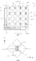
- a capacitive touch panel 10 comprises a transparent substrate 1, a sensing circuit layer 2, a protective layer 4, and a black matrix 5.
- the upper surface 11 of the transparent substrate 1 is used for touching while the sensing circuit layer 2 is set on the lower surface 12 and surface of the sensing circuit layer 2 is covered by the protective layer 4.
- the sensing circuit layer 2 comprises a plurality of first-axis electrodes 21 and second-axis electrodes 22, located on X-axis and Y-axis of the vertical coordinate axes respectively.
- Each first-axis electrode 21 has a plurality of first electrodes 211 and first-axis wires 212 connected to two adjacent first electrodes 211.
- Each second-axis electrode 22 has a plurality of second electrodes 221 and second-axis wires 222 connected to two adjacent second electrodes 221.
- Lower surfaces of the first-axis wires 212 have insulating sheets 31, by which the first-axis wires 212 and the second-axis wires 222 are insulated.
- Metal circuits 23 for transmitting signals are set around the sensing circuit layer 2.
- the black matrix 5 is laminated around the lower surface 12 of the transparent substrate to cover the metal circuits 23.
- Transparent conductive materials such as indium tin oxide (ITO) and antimony tin oxide (ATO) are usually used in practical production.
- ITO indium tin oxide
- ATO antimony tin oxide
- the first electrodes 211, first-axis wires 212, and the second electrodes 221 are formed synchronously on the lower surface 12 of the transparent substrate 1.
- the insulating sheets 31 are then set on the lower surfaces of the first-axis wires 212, and the second-axis wires 222 are set across the insulating sheets 31 and connect two adjacent second electrodes 221.
- metal jumpers Due to good electrical conductivity and low cost of metal materials (such as aluminum, silver, chromium, copper, etc.), metal wires (metal jumpers), which are made of metal materials, are usually selected for the second-axis wires 222.
- metal jumpers have a certain width, and reflectance of metal materials is relatively high, which is different from the surrounding transparent conductive material and the transparent substrate, and therefore human eyes can perceive the obvious difference, leading to the product's defective appearance with the metal jumpers being visible.
- the method adopted in the existing technology is mainly to reduce exterior sizes of the metal jumpers and making the line width very small.
- this method is hard to be realized, easy to cause reduction in production yield, and unable to completely eliminate the problem that the metal jumpers are visible on the touch panel.
- a capacitive touch panel comprises a transparent substrate and at least one metal jumper.
- a mask layer, reflectance of which is lower than that of the metal jumper, is set between the metal jumper and the transparent substrate to block the light reflected by the metal jumper.
- the transparent substrate has a first surface available for touching and a second surface opposite to the first surface.
- the capacitive touch panel also comprises a sensing circuit layer used to sense the touch and generate sense signals.
- the sensing circuit layer is placed on the second surface of the transparent substrate, comprising at least a plurality of first electrodes and a plurality of second electrodes. Adjacent first electrodes are electrically connected through a first-axis wire.
- the metal jumper is set between the adjacent second electrodes to electrically connect the adjacent second electrodes while the metal jumper and the first electrodes are electrically insulated.
- the mask layer is placed on the second surface of the transparent substrate, comprising at least one mask piece. Location and size of the mask piece correspond to those of the metal jumper.
- the mask layer can also be used as an insulating sheet, placed on the metal jumper. Width of the insulating sheet is less than the length of the metal jumper but not less than the width of the metal jumper.
- the mask layer is made of grey, brown or black non-conductive mask material, comprising black photoresistive material, brown photoresistive material, grey photoresistive material, nitride, oxide or mixture of nitride and oxide.
- the method Before placing the metal jumper on the second surface of the transparent substrate, the method also comprises the following step: placing a sensing circuit layer on the second surface of the transparent substrate, wherein the sensing circuit layer comprises at least two electrodes and the metal jumper is connected between the two electrodes.
- the mask layer is made of grey, brown or black non-conductive mask material, comprising black photoresistive material, brown photoresistive material, grey photoresistive material, nitride, oxide or mixture of nitride and oxide.
- a mask layer is added between the transparent substrate and the metal jumper.
- the mask layer is made of black or melanocratic non-conductive materials, which can reduce light reflection of the metal jumper and reduce visibility of the metal jumper so that it is not easy to be perceived by human eyes thereby making the capacitive touch panel a good visual effect.
- the method for reducing visibility of the metal jumper in a capacitive touch panel provided in the present invention, it can improve the optical characteristics and appearance effect of the product without adding additional process while the cost is almost not increased.
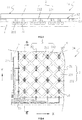
- a capacitive touch panel 10 comprises a transparent substrate 1, a sensing circuit layer 2, a protective layer 4, a black matrix 5 and a mask layer 6.
- the sensing circuit layer 2 is set between the transparent substrate 1 and the protective layer 4, and is placed on the lower surface 12 of the transparent substrate 1 while the upper surface 11 is used for touching.
- the sensing circuit layer 2 comprises a plurality of first-axis electrodes 21 and second-axis electrodes 22, located on X-axis and Y-axis of the vertical coordinate axes respectively.
- Each first-axis electrode 21 has a plurality of first electrodes 211 and first-axis wires 212 connected to two adjacent first electrodes 211; each second-axis electrode 22 has a plurality of second electrodes 221 and second-axis wires 222 connected to two adjacent second electrodes 221.
- Metal jumpers are usually used for the second-axis wires 222; the first-axis wires 212 and the second-axis wires 222 are insulated by the insulating sheets 31.
- the mask layer 6 is laminated on the lower surface 12 of the transparent substrate 1 and divided into a plurality of mask pieces 6a.
- each mask piece 6a corresponds to those of the second-axis wire 222 (metal jumper), and the reflectance is lower than that of the metal jumper so as to reduce light reflection of the metal jumper and reduce visibility of the metal jumper.
- Metal circuits 23 used for transmitting signals are set around the sensing circuit layer 2.
- the black matrix 5 is laminated around the lower surface 12 of the transparent substrate to cover the metal circuits 23 so that the metal circuits 23 are not exposed on the surface of the transparent substrate 1, beautifying the touch panel's appearance.
- the first electrodes 211, first-axis wires 212, and the second electrodes 221 are formed synchronously on the lower surface 12 of the transparent substrate 1.
- the insulating sheets 31 are then set on the lower surfaces of the first-axis wires 212 and the metal jumpers, acting as the second-axis wires 222, are set across the insulating sheets 31, wherein the metal jumpers connect two adjacent second electrodes 221.
- the insulating sheets 31 are placed between two adjacent second electrodes 221 on the same axis, and width (along Y-axis) of the insulating sheets 31 is more than width (along Y-axis) of the first-axis wires 212 but less than length (along Y-axis) of the second-axis wires 222.
- width (along Y-axis) of the insulating sheets 31 should not be less than the distance between two adjacent second electrodes 221.
- a mask layer 6 is set between the metal jumpers and the transparent substrate 1 to avoid the metal jumpers from getting laminated directly on the transparent substrate 1.
- width of the insulating sheets 31 which means that the width not only can be more than the distance between two adjacent second electrodes 221 but also can be less than or equal to the distance. Meanwhile, covering areas of the insulating sheets 31 can be narrowed correspondingly to reduce length of the metal jumpers so that the metal jumpers are less easily seen.
- Fig. 6B demonstrates yet another schematic sectional view of the capacitive touch panel 10 in accordance with the first embodiment. It is similar to the above structure, but the difference lies in the width of the insulating sheets 31, wherein the width is less than the distance between two adjacent second electrodes 221.
- the insulating sheets 31 are covered on the surface of the first-axis wires 212.
- the metal jumpers, acting as the second-axis wires 222, are covered on the surface of the insulating sheets 31 and connect two adjacent second electrodes 221.
- the transparent substrate 1 is made of transparent non-conductive materials such as glass, PMMA, PVC, PP and PET, etc.
- the insulating sheets 31 are made of insulating materials such as silicon dioxide.
- the black matrix 5 and the mask layer 6 are made of black, grey or brown non-conductive materials, such as black photoresistive material, brown photoresistive material, grey photoresistive material, nitride, oxide or mixture of nitride and oxide.
- the mask layer 6 is made up of a plurality of mask pieces 6a which are set separately, wherein because the mask pieces 6a are very short and narrow with an area of 10 -4 mm 2 , they are not easy for people to discern them. Therefore, adding mask pieces can effectively block the light reflected by the metal jumpers and produce a good appearance of the touch panel.
- a protective layer 7 that shields electromagnetic noise can also be set between the black matrix 5 and the transparent substrate 1.
- a mask layer 6 can be added on the metal jumper to reduce the light reflected by the metal jumper and thereby reduce visibility of the metal jumper. Therefore, appearance effect of the transparent touch panel is improved.
- Structure of multi-layer sensing circuit layer can be adopted for the sensing circuit layer 2 and set based on the actual using requirement.
- a mask layer 6 is coated on the second surface 12 of the transparent substrate 1, comprising a plurality of mask pieces 6a set on the second surface 12 of the transparent substrate 1 at certain intervals.
- a transparent conducting layer is coated on the second surface 12 of the transparent substrate 1, forming a sensing circuit layer 2 with electrode pattern, wherein the sensing circuit layer 2 comprises a plurality of first electrodes 211, second electrodes 221, and first-axis wires 212 connected to two adjacent first electrodes 211.
- the insulating sheets 31 are then placed on the first-axis wires 212 by using transparent insulating materials after which the corresponding metal jumpers 222 and metal circuits 23 can be set, wherein the metal jumpers 222 are set across the insulating sheets 31 and configured to connect two adjacent second electrodes 221 on the same axis.
- locations of the metal jumpers correspond to locations of the mask pieces 6a respectively.
- the metal circuits 23 are placed around the sensing circuit layer 2 for transmitting signals and finally, a protective layer 4 using silicon dioxide, organic polymer or other materials is set on the electrode layer 2.
- a black matrix 5 can be coated around the second surface 12 of the transparent substrate 1 synchronously, and the black matrix 5 corresponds to the metal circuits 23.
- the mask layer 6 is made synchronously with the black matrix 5 so that the appearance can be improved without increasing the cost. If a protective layer 7 needs to be added, the protective layer 7, usually made of metal materials, should be placed on the edge of the transparent substrate 1 before setting the mask layer 6 and the black matrix 5.
- the structure is similar to the first embodiment and comprises of a transparent substrate 1, a sensing circuit layer 2, a protective layer 4, a black matrix 5, and a mask layer 6.
- First electrodes 211, first-axis wires 212, and second electrodes 221 of the sensing circuit layer 2 are placed on a second surface 12 of the transparent substrate 1.
- Second-axis wires 222 are metal jumpers; the first-axis wires 212 and the metal jumpers are insulated by insulating sheets 31.
- the insulating sheets 31 are made of black or melanocratic insulating materials, act as a mask layer, and are placed above the metal jumpers.
- Width (along Y-axis) of the insulating sheets 31 is more than width (along Y-axis) of the first-axis wires 212 but less than length (along Y-axis) of the second-axis wires 222.
- Length (along X-axis) of the insulating sheets 31 is not less than the width (along X-axis) of the second-axis wires 222 so that the metal jumpers are insulated from the first-axis wires 212 and connect two adjacent second electrodes 221. In this way, the insulating sheets 31 can reduce light reflection of the metal jumpers so as to reduce visibility of the metal jumpers.
- Production of the capacitive touch panel comprises the following steps:
- a transparent conducting layer is coated on the second surface 12 of the transparent substrate 1.
- a sensing circuit layer 2 is formed with an electrode pattern after a etching process, wherein the electrode pattern comprises of a plurality of first electrodes 211, second electrodes 221, and first-axis wires 212, which are connected to two adjacent first electrodes 211.
- Insulating sheets 31 can be placed on the first-axis wires 212 by using melanocratic or black insulating materials, wherein the insulating sheets 31 act as mask pieces; and then metal jumpers 222 and metal circuits 23 are set.
- the metal jumpers 222 are set across the insulating sheets 31 and connect two adjacent second electrodes 221.
- the metal circuits 23 are placed around the sensing circuit layer 2 for transmitting signals.
- Melanocratic or black insulating materials can be organic insulating materials, such as black phenolic resin.
- a black matrix 5 should be coated around the second surface 12 of the transparent substrate 1, location of which corresponds to that of the metal circuits 23 to cover the metal circuits 23 so that the metal circuits 23 are not exposed on the surface of the transparent substrate 1, beautifying the touch panel's appearance.
- the capacitive touch panel 10 comprises a transparent substrate 1, a sensing circuit layer 2, a protective layer 4, a black matrix 5, a mask layer 6, and an insulating layer 3, which has a plurality of through-holes 32.
- First-axis electrodes 21 and second-axis electrodes 22 are located on first surface 33 of the insulating layer 3.
- Each first-axis electrode 21 has a plurality of first electrodes 211 and first-axis wires 212, which connect two adjacent first electrodes 211.
- Each second-axis electrode 22 has a plurality of second electrodes 221 placed between two corresponding adjacent first-axis electrodes 21, interlacing with the first electrodes 211 at intervals; each second-axis electrode 22 also has a plurality of second-axis wires 222 which are metal jumpers set on the second surface 34 of the insulating layer 3, opposite to the first surface 33. Both ends of each metal jumper pass through the corresponding through-holes 32 respectively and connect the two adjacent second electrodes 221. Location and size of the metal jumper correspond to those of the mask layer 6.
- Production of the capacitive touch panel comprises the following steps:
- a mask layer 6 is coated on the second surface 12 of the transparent substrate 1, wherein the mask layer 6 comprises of a plurality of mask pieces 6a set on the second surface 12 of the transparent substrate 1 at certain intervals.
- a transparent conducting layer is coated on the second surface 12 of the transparent substrate 1.
- a sensing circuit layer 2 is then formed with electrode pattern, wherein the sensing circuit layer 2 comprises a plurality of first electrodes 211, second electrodes 221, and first-axis wires 212, which are connected to two adjacent first electrodes 211.
- An insulating layer 3 is placed on the sensing circuit layer 2 by using transparent insulting materials and a plurality of through-holes 32 are formed on the second electrodes 221. Then second-axis wires 222 (metal jumpers) and metal circuits 23 are set.
- both ends of the metal jumpers pass through the corresponding through-holes 32 respectively and connect the two adjacent second electrodes 221.
- the metal circuits 23 are placed around the sensing circuit layer 2 for transmitting signals.
- black matrix 5 can be coated around the second surface 12 of the transparent substrate 1 synchronously; the black matrix 5 is covered around the second surface 12 of the transparent substrate 1, location of which corresponds to that of the metal circuits 23.
Landscapes
- Engineering & Computer Science (AREA)
- General Engineering & Computer Science (AREA)
- Theoretical Computer Science (AREA)
- Human Computer Interaction (AREA)
- Physics & Mathematics (AREA)
- General Physics & Mathematics (AREA)
- Position Input By Displaying (AREA)
- Switches That Are Operated By Magnetic Or Electric Fields (AREA)
Applications Claiming Priority (1)
| Application Number | Priority Date | Filing Date | Title |
|---|---|---|---|
| CN2011102350167A CN102929454A (zh) | 2011-08-12 | 2011-08-12 | 电容式触控面板及降低其金属导体可见度的方法 |
Publications (2)
| Publication Number | Publication Date |
|---|---|
| EP2557487A2 true EP2557487A2 (fr) | 2013-02-13 |
| EP2557487A3 EP2557487A3 (fr) | 2014-04-02 |
Family
ID=45811359
Family Applications (1)
| Application Number | Title | Priority Date | Filing Date |
|---|---|---|---|
| EP12158344.7A Withdrawn EP2557487A3 (fr) | 2011-08-12 | 2012-03-07 | Panneau tactile capacitif et son procédé de fabrication |
Country Status (7)
| Country | Link |
|---|---|
| US (1) | US9489090B2 (fr) |
| EP (1) | EP2557487A3 (fr) |
| JP (2) | JP2013041573A (fr) |
| KR (1) | KR101479376B1 (fr) |
| CN (1) | CN102929454A (fr) |
| DE (1) | DE202012013529U1 (fr) |
| TW (2) | TWI585659B (fr) |
Cited By (4)
| Publication number | Priority date | Publication date | Assignee | Title |
|---|---|---|---|---|
| CN103472945A (zh) * | 2013-08-19 | 2013-12-25 | 南昌欧菲光科技有限公司 | 触摸屏用触控元件及其制造方法 |
| EP2843517A1 (fr) * | 2013-08-27 | 2015-03-04 | LG Innotek Co., Ltd. | Panneau tactile et affichage |
| CN104898886A (zh) * | 2015-06-19 | 2015-09-09 | 京东方科技集团股份有限公司 | 一种基板及其制备方法、触控显示屏 |
| US9477355B2 (en) | 2013-09-04 | 2016-10-25 | Lg Innotek Co., Ltd. | Touch panel and display |
Families Citing this family (37)
| Publication number | Priority date | Publication date | Assignee | Title |
|---|---|---|---|---|
| CN104246611B (zh) * | 2012-03-30 | 2018-12-04 | 富士胶片株式会社 | 黑色树脂膜、静电电容型输入装置及它们的制造方法及具备其的图像显示装置 |
| KR20130119762A (ko) * | 2012-04-24 | 2013-11-01 | 삼성전기주식회사 | 터치패널 |
| TWI460629B (zh) * | 2012-05-11 | 2014-11-11 | Au Optronics Corp | 觸控顯示面板及其製造方法 |
| JP5887314B2 (ja) * | 2012-09-19 | 2016-03-16 | 富士フイルム株式会社 | 静電容量型入力装置の製造方法および静電容量型入力装置、並びに、これを備えた画像表示装置 |
| KR101976637B1 (ko) | 2012-10-11 | 2019-05-10 | 엘지이노텍 주식회사 | 터치 패널 및 이의 제조방법 |
| TWI486857B (zh) * | 2012-12-19 | 2015-06-01 | Chih Chung Lin | 觸控模組 |
| TWM457919U (zh) * | 2013-02-08 | 2013-07-21 | Liyitec Inc | 觸控面板 |
| CN103208326B (zh) * | 2013-03-30 | 2014-12-17 | 深圳欧菲光科技股份有限公司 | 导电膜及其制备方法以及包含该导电膜的触摸屏 |
| US9089061B2 (en) | 2013-03-30 | 2015-07-21 | Shenzhen O-Film Tech Co., Ltd. | Conductive film, method for making the same, and touch screen including the same |
| CN103198885B (zh) * | 2013-03-30 | 2014-12-17 | 深圳欧菲光科技股份有限公司 | 导电膜及其制备方法以及包含该导电膜的触摸屏 |
| US9538654B2 (en) | 2013-03-30 | 2017-01-03 | Shenzhen O-Film Tech Co., Ltd. | Conductive film, method for manufacturing the same, and touch screen including the same |
| TWI502425B (zh) * | 2013-04-25 | 2015-10-01 | Au Optronics Corp | 觸控面板及使用其之觸控顯示面板 |
| CN104142749B (zh) * | 2013-05-09 | 2018-01-02 | 祥达光学(厦门)有限公司 | 一种触控面板及其制作方法 |
| CN104156127A (zh) * | 2013-05-13 | 2014-11-19 | 胜华科技股份有限公司 | 触控面板 |
| TWI485598B (zh) * | 2013-07-02 | 2015-05-21 | Au Optronics Corp | 觸控面板及其製造方法 |
| TWI503713B (zh) * | 2013-07-17 | 2015-10-11 | Hannstouch Solution Inc | 觸控面板 |
| JP6339780B2 (ja) * | 2013-08-27 | 2018-06-06 | エルジー イノテック カンパニー リミテッド | タッチパネル及びディスプレイ |
| CN104423667B (zh) * | 2013-08-30 | 2018-01-12 | Lg伊诺特有限公司 | 触摸板和显示器 |
| JP5848736B2 (ja) * | 2013-09-06 | 2016-01-27 | デクセリアルズ株式会社 | 静電容量型タッチパネル |
| KR102116483B1 (ko) * | 2013-10-18 | 2020-05-29 | 삼성디스플레이 주식회사 | 터치 스크린 패널 및 그 제조방법 |
| CN103995611B (zh) * | 2014-04-08 | 2017-02-01 | 业成光电(深圳)有限公司 | 可降低反射视效的触控结构及其方法 |
| TWI599679B (zh) * | 2014-04-22 | 2017-09-21 | 達興材料股份有限公司 | 形成金屬導線的方法 |
| TW201545030A (zh) | 2014-05-30 | 2015-12-01 | Henghao Technology Co Ltd | 觸控面板及其形成方法 |
| US20160026292A1 (en) * | 2014-07-28 | 2016-01-28 | Eturbotouch Technology Inc. | Circuit connection structure of touch sensor panel |
| US20160026284A1 (en) * | 2014-07-28 | 2016-01-28 | Eturbotouch Technology Inc. | Circuit connection structure of touch sensor panel |
| EP3007109B1 (fr) * | 2014-10-06 | 2016-12-07 | T-Touch International S.à.r.l. | Support d'informations avec une précision de détection améliorée par une accumulation multicouche du support d'informations |
| KR101942294B1 (ko) * | 2014-12-09 | 2019-01-25 | 동우 화인켐 주식회사 | 터치 스크린 패널 및 이를 구비하는 화상표시장치 |
| JP6506119B2 (ja) * | 2015-06-29 | 2019-04-24 | グンゼ株式会社 | タッチ入力装置 |
| TWI599928B (zh) * | 2016-01-18 | 2017-09-21 | 友達光電股份有限公司 | 顯示裝置及其製作方法 |
| KR102556838B1 (ko) * | 2016-06-01 | 2023-07-19 | 삼성디스플레이 주식회사 | 터치 패널, 이를 포함하는 전자 장치, 및 터치 패널 제조 방법 |
| CN106886338B (zh) * | 2017-02-08 | 2023-03-10 | 江西卓讯微电子有限公司 | 触摸屏及电子装置 |
| CN107252323B (zh) * | 2017-06-05 | 2020-06-26 | 厦门美柚股份有限公司 | 女性生理周期的预测方法、装置及用户设备 |
| CN207182255U (zh) * | 2017-09-18 | 2018-04-03 | 汕头超声显示器有限公司 | 一种减少侧光反射的电容触摸屏 |
| KR102374754B1 (ko) * | 2017-09-27 | 2022-03-15 | 엘지디스플레이 주식회사 | 터치 구조물을 포함하는 디스플레이 장치 |
| US11269416B2 (en) * | 2017-11-15 | 2022-03-08 | Google Llc | Touch communication device |
| TWI686738B (zh) | 2019-04-24 | 2020-03-01 | 友達光電股份有限公司 | 觸控顯示裝置 |
| CN111613629B (zh) * | 2020-06-28 | 2022-09-09 | 武汉华星光电技术有限公司 | 一种导电膜层、导电膜层制备方法及显示装置 |
Citations (2)
| Publication number | Priority date | Publication date | Assignee | Title |
|---|---|---|---|---|
| US20100295819A1 (en) * | 2009-05-19 | 2010-11-25 | Optrex Corporation | Connection structure between electrodes and touch panel |
| CN101576794B (zh) * | 2009-06-05 | 2011-05-18 | 深圳莱宝高科技股份有限公司 | 一种电容式触摸屏及其制造方法 |
Family Cites Families (32)
| Publication number | Priority date | Publication date | Assignee | Title |
|---|---|---|---|---|
| US4320418A (en) * | 1978-12-08 | 1982-03-16 | Pavliscak Thomas J | Large area display |
| US5229691A (en) * | 1991-02-25 | 1993-07-20 | Panocorp Display Systems | Electronic fluorescent display |
| US6605826B2 (en) * | 2000-08-18 | 2003-08-12 | Semiconductor Energy Laboratory Co., Ltd. | Light-emitting device and display device |
| US7190416B2 (en) * | 2002-10-18 | 2007-03-13 | Nitto Denko Corporation | Liquid crystal display with touch panel having internal front polarizer |
| JP4511307B2 (ja) * | 2004-02-10 | 2010-07-28 | セイコーエプソン株式会社 | ゲート絶縁膜、半導体素子、電子デバイスおよび電子機器 |
| KR101383717B1 (ko) * | 2007-06-27 | 2014-04-10 | 삼성디스플레이 주식회사 | 표시 장치 및 그 제조 방법 |
| CN100495139C (zh) * | 2007-10-10 | 2009-06-03 | 友达光电股份有限公司 | 触控面板及其制作方法 |
| TWM348999U (en) * | 2008-02-18 | 2009-01-11 | Tpk Touch Solutions Inc | Capacitive touch panel |
| JP2009265748A (ja) | 2008-04-22 | 2009-11-12 | Hitachi Displays Ltd | タッチパネル付き表示装置 |
| CN102112950B (zh) * | 2008-09-12 | 2015-01-28 | 奥博特瑞克斯株式会社 | 电容型触摸面板、显示装置及电容型触摸面板的制造方法 |
| TWI380089B (en) * | 2008-12-03 | 2012-12-21 | Au Optronics Corp | Method of forming a color filter touch sensing substrate |
| CN201352342Y (zh) | 2008-12-19 | 2009-11-25 | 洋华光电股份有限公司 | 改进的电容式触控感测结构 |
| TWI373665B (en) * | 2008-12-25 | 2012-10-01 | Au Optronics Corp | Touch panel structure |
| CN101464761A (zh) | 2009-01-05 | 2009-06-24 | 中国南玻集团股份有限公司 | 电容式触控屏 |
| KR101219242B1 (ko) * | 2009-01-16 | 2013-01-07 | 삼성디스플레이 주식회사 | 터치 스크린 패널 및 그 제조방법 |
| US8593410B2 (en) * | 2009-04-10 | 2013-11-26 | Apple Inc. | Touch sensor panel design |
| TW201040818A (en) * | 2009-05-08 | 2010-11-16 | Sintek Photronic Corp | Capacitive touch panel structure with high optical uniformity |
| JP2011018885A (ja) * | 2009-06-12 | 2011-01-27 | Seiko Epson Corp | パターン膜形成部材の製造方法、パターン膜形成部材、電気光学装置、電子機器 |
| WO2011017039A2 (fr) * | 2009-08-03 | 2011-02-10 | 3M Innovative Properties Company | Filtre optique de blindage anti-interférences électromagnétiques (iem) transparent et antiréfléchissant |
| CN101989160A (zh) * | 2009-08-07 | 2011-03-23 | 铼宝科技股份有限公司 | 电容式触控面板 |
| JP5372697B2 (ja) | 2009-10-21 | 2013-12-18 | 京セラディスプレイ株式会社 | 投影型静電容量タッチパネルの製造方法 |
| JP2011128674A (ja) | 2009-12-15 | 2011-06-30 | Sony Corp | 静電容量型入力装置およびその製造方法 |
| CN201600670U (zh) * | 2009-12-22 | 2010-10-06 | 洋华光电股份有限公司 | 触控面板 |
| KR101821429B1 (ko) * | 2009-12-29 | 2018-01-23 | 퀄컴 엠이엠에스 테크놀로지스, 인크. | 금속화된 광 방향 전환 특징부를 갖는 조명 장치 |
| TW201124766A (en) * | 2010-01-08 | 2011-07-16 | Wintek Corp | Display device with touch panel |
| TWI435140B (zh) * | 2010-04-09 | 2014-04-21 | Wintek Corp | 觸控顯示面板 |
| KR101100949B1 (ko) * | 2010-04-28 | 2011-12-29 | 삼성모바일디스플레이주식회사 | 터치 스크린 패널 및 이를 구비한 영상표시장치 |
| CN102279678A (zh) * | 2010-06-12 | 2011-12-14 | 宸鸿科技(厦门)有限公司 | 触控电路图形结构及制造方法、触控面板及触控显示屏 |
| KR101314779B1 (ko) * | 2010-08-18 | 2013-10-08 | 엘지디스플레이 주식회사 | 정전용량 방식 터치 스크린 패널 및 그 제조방법 |
| TW201213949A (en) * | 2010-09-29 | 2012-04-01 | Catcher Technology Co Ltd | Touch panel |
| TWI439896B (zh) * | 2011-01-14 | 2014-06-01 | Chunghwa Picture Tubes Ltd | 觸控面板之感應裝置 |
| CN202351840U (zh) * | 2011-08-12 | 2012-07-25 | 宸鸿科技(厦门)有限公司 | 电容式触控面板 |
-
2011
- 2011-08-12 CN CN2011102350167A patent/CN102929454A/zh active Pending
-
2012
- 2012-02-22 TW TW101105832A patent/TWI585659B/zh not_active IP Right Cessation
- 2012-02-22 TW TW101203212U patent/TWM434264U/zh not_active IP Right Cessation
- 2012-02-29 US US13/409,023 patent/US9489090B2/en active Active
- 2012-03-07 DE DE202012013529.5U patent/DE202012013529U1/de not_active Expired - Lifetime
- 2012-03-07 EP EP12158344.7A patent/EP2557487A3/fr not_active Withdrawn
- 2012-03-12 KR KR20120025069A patent/KR101479376B1/ko active Active
- 2012-06-06 JP JP2012128527A patent/JP2013041573A/ja active Pending
-
2014
- 2014-12-04 JP JP2014245865A patent/JP2015079526A/ja active Pending
Patent Citations (2)
| Publication number | Priority date | Publication date | Assignee | Title |
|---|---|---|---|---|
| US20100295819A1 (en) * | 2009-05-19 | 2010-11-25 | Optrex Corporation | Connection structure between electrodes and touch panel |
| CN101576794B (zh) * | 2009-06-05 | 2011-05-18 | 深圳莱宝高科技股份有限公司 | 一种电容式触摸屏及其制造方法 |
Cited By (5)
| Publication number | Priority date | Publication date | Assignee | Title |
|---|---|---|---|---|
| CN103472945A (zh) * | 2013-08-19 | 2013-12-25 | 南昌欧菲光科技有限公司 | 触摸屏用触控元件及其制造方法 |
| EP2843517A1 (fr) * | 2013-08-27 | 2015-03-04 | LG Innotek Co., Ltd. | Panneau tactile et affichage |
| US9477355B2 (en) | 2013-09-04 | 2016-10-25 | Lg Innotek Co., Ltd. | Touch panel and display |
| CN104898886A (zh) * | 2015-06-19 | 2015-09-09 | 京东方科技集团股份有限公司 | 一种基板及其制备方法、触控显示屏 |
| US10133379B2 (en) | 2015-06-19 | 2018-11-20 | Boe Technology Group Co., Ltd. | Substrate, touch display panel having the same, and method thereof |
Also Published As
| Publication number | Publication date |
|---|---|
| TW201308176A (zh) | 2013-02-16 |
| JP2015079526A (ja) | 2015-04-23 |
| US9489090B2 (en) | 2016-11-08 |
| EP2557487A3 (fr) | 2014-04-02 |
| KR20130018100A (ko) | 2013-02-20 |
| TWI585659B (zh) | 2017-06-01 |
| DE202012013529U1 (de) | 2017-06-27 |
| JP2013041573A (ja) | 2013-02-28 |
| TWM434264U (en) | 2012-07-21 |
| CN102929454A (zh) | 2013-02-13 |
| KR101479376B1 (ko) | 2015-01-05 |
| US20130038571A1 (en) | 2013-02-14 |
Similar Documents
| Publication | Publication Date | Title |
|---|---|---|
| US9489090B2 (en) | Capacitive touch panel and a method of manufacturing the same | |
| US9454267B2 (en) | Touch sensing circuit and method for making the same | |
| US10691266B2 (en) | Touch panel stackup | |
| US8698001B2 (en) | Electrode structure of the touch panel, method thereof and touch panel | |
| US10048783B2 (en) | Touch panel device | |
| US9483145B2 (en) | Touch panel and a manufacturing method thereof | |
| US10048820B2 (en) | Touch panel and manufacturing method thereof | |
| CN103186271B (zh) | 触控面板及其制作方法 | |
| US10831295B2 (en) | Touch screen, touch panel, display device, and electronic apparatus | |
| US20120169626A1 (en) | Touch panel and touch display panel | |
| US10359890B2 (en) | Touch screen, touch panel, and display apparatus | |
| WO2018110123A1 (fr) | Capteur et dispositif de type capacitif | |
| CN205507728U (zh) | 触控面板 | |
| CN202351840U (zh) | 电容式触控面板 | |
| US9760230B2 (en) | Touch screen, touch panel, display device, and electronic device | |
| US20140177137A1 (en) | Touch panel | |
| JP2015210554A (ja) | タッチスクリーン、タッチパネル、表示装置、および電子機器 |
Legal Events
| Date | Code | Title | Description |
|---|---|---|---|
| PUAI | Public reference made under article 153(3) epc to a published international application that has entered the european phase |
Free format text: ORIGINAL CODE: 0009012 |
|
| AK | Designated contracting states |
Kind code of ref document: A2 Designated state(s): AL AT BE BG CH CY CZ DE DK EE ES FI FR GB GR HR HU IE IS IT LI LT LU LV MC MK MT NL NO PL PT RO RS SE SI SK SM TR |
|
| AX | Request for extension of the european patent |
Extension state: BA ME |
|
| PUAL | Search report despatched |
Free format text: ORIGINAL CODE: 0009013 |
|
| AK | Designated contracting states |
Kind code of ref document: A3 Designated state(s): AL AT BE BG CH CY CZ DE DK EE ES FI FR GB GR HR HU IE IS IT LI LT LU LV MC MK MT NL NO PL PT RO RS SE SI SK SM TR |
|
| AX | Request for extension of the european patent |
Extension state: BA ME |
|
| RIC1 | Information provided on ipc code assigned before grant |
Ipc: G06F 3/044 20060101AFI20140227BHEP |
|
| 17P | Request for examination filed |
Effective date: 20140929 |
|
| STAA | Information on the status of an ep patent application or granted ep patent |
Free format text: STATUS: EXAMINATION IS IN PROGRESS |
|
| 17Q | First examination report despatched |
Effective date: 20170127 |
|
| STAA | Information on the status of an ep patent application or granted ep patent |
Free format text: STATUS: THE APPLICATION HAS BEEN WITHDRAWN |
|
| 18W | Application withdrawn |
Effective date: 20170530 |