EP2557569A1 - Feldprogrammierbare Festwertspeichervorrichtung - Google Patents
Feldprogrammierbare Festwertspeichervorrichtung Download PDFInfo
- Publication number
- EP2557569A1 EP2557569A1 EP11306028A EP11306028A EP2557569A1 EP 2557569 A1 EP2557569 A1 EP 2557569A1 EP 11306028 A EP11306028 A EP 11306028A EP 11306028 A EP11306028 A EP 11306028A EP 2557569 A1 EP2557569 A1 EP 2557569A1
- Authority
- EP
- European Patent Office
- Prior art keywords
- nanotube
- fprom
- connecting element
- moveable
- memory
- Prior art date
- Legal status (The legal status is an assumption and is not a legal conclusion. Google has not performed a legal analysis and makes no representation as to the accuracy of the status listed.)
- Withdrawn
Links
- 230000003068 static effect Effects 0.000 claims abstract description 33
- 239000002071 nanotube Substances 0.000 claims description 77
- 239000000853 adhesive Substances 0.000 claims description 16
- 230000001070 adhesive effect Effects 0.000 claims description 16
- 239000003292 glue Substances 0.000 claims description 3
- 210000004027 cell Anatomy 0.000 description 29
- 230000014759 maintenance of location Effects 0.000 description 7
- 230000005684 electric field Effects 0.000 description 6
- 230000007774 longterm Effects 0.000 description 5
- 239000003795 chemical substances by application Substances 0.000 description 4
- 210000000352 storage cell Anatomy 0.000 description 4
- 239000013043 chemical agent Substances 0.000 description 3
- 238000006243 chemical reaction Methods 0.000 description 3
- 238000005516 engineering process Methods 0.000 description 3
- 230000005672 electromagnetic field Effects 0.000 description 2
- 238000004519 manufacturing process Methods 0.000 description 2
- 230000035939 shock Effects 0.000 description 2
- 239000002109 single walled nanotube Substances 0.000 description 2
- 238000005411 Van der Waals force Methods 0.000 description 1
- 239000007795 chemical reaction product Substances 0.000 description 1
- 238000013500 data storage Methods 0.000 description 1
- 230000006870 function Effects 0.000 description 1
- 238000000034 method Methods 0.000 description 1
- 239000000047 product Substances 0.000 description 1
Images


Classifications
-
- G—PHYSICS
- G11—INFORMATION STORAGE
- G11C—STATIC STORES
- G11C17/00—Read-only memories programmable only once; Semi-permanent stores, e.g. manually-replaceable information cards
- G11C17/14—Read-only memories programmable only once; Semi-permanent stores, e.g. manually-replaceable information cards in which contents are determined by selectively establishing, breaking or modifying connecting links by permanently altering the state of coupling elements, e.g. PROM
-
- B—PERFORMING OPERATIONS; TRANSPORTING
- B82—NANOTECHNOLOGY
- B82Y—SPECIFIC USES OR APPLICATIONS OF NANOSTRUCTURES; MEASUREMENT OR ANALYSIS OF NANOSTRUCTURES; MANUFACTURE OR TREATMENT OF NANOSTRUCTURES
- B82Y10/00—Nanotechnology for information processing, storage or transmission, e.g. quantum computing or single electron logic
-
- G—PHYSICS
- G11—INFORMATION STORAGE
- G11C—STATIC STORES
- G11C13/00—Digital stores characterised by the use of storage elements not covered by groups G11C11/00, G11C23/00, or G11C25/00
- G11C13/02—Digital stores characterised by the use of storage elements not covered by groups G11C11/00, G11C23/00, or G11C25/00 using elements whose operation depends upon chemical change
- G11C13/025—Digital stores characterised by the use of storage elements not covered by groups G11C11/00, G11C23/00, or G11C25/00 using elements whose operation depends upon chemical change using fullerenes, e.g. C60, or nanotubes, e.g. carbon or silicon nanotubes
-
- G—PHYSICS
- G11—INFORMATION STORAGE
- G11C—STATIC STORES
- G11C17/00—Read-only memories programmable only once; Semi-permanent stores, e.g. manually-replaceable information cards
-
- G—PHYSICS
- G11—INFORMATION STORAGE
- G11C—STATIC STORES
- G11C23/00—Digital stores characterised by movement of mechanical parts to effect storage, e.g. using balls; Storage elements therefor
-
- H—ELECTRICITY
- H10—SEMICONDUCTOR DEVICES; ELECTRIC SOLID-STATE DEVICES NOT OTHERWISE PROVIDED FOR
- H10D—INORGANIC ELECTRIC SEMICONDUCTOR DEVICES
- H10D62/00—Semiconductor bodies, or regions thereof, of devices having potential barriers
- H10D62/10—Shapes, relative sizes or dispositions of the regions of the semiconductor bodies; Shapes of the semiconductor bodies
- H10D62/117—Shapes of semiconductor bodies
- H10D62/118—Nanostructure semiconductor bodies
-
- H—ELECTRICITY
- H10—SEMICONDUCTOR DEVICES; ELECTRIC SOLID-STATE DEVICES NOT OTHERWISE PROVIDED FOR
- H10K—ORGANIC ELECTRIC SOLID-STATE DEVICES
- H10K85/00—Organic materials used in the body or electrodes of devices covered by this subclass
- H10K85/20—Carbon compounds, e.g. carbon nanotubes or fullerenes
- H10K85/221—Carbon nanotubes
-
- G—PHYSICS
- G11—INFORMATION STORAGE
- G11C—STATIC STORES
- G11C2213/00—Indexing scheme relating to G11C13/00 for features not covered by this group
- G11C2213/10—Resistive cells; Technology aspects
- G11C2213/16—Memory cell being a nanotube, e.g. suspended nanotube
-
- G—PHYSICS
- G11—INFORMATION STORAGE
- G11C—STATIC STORES
- G11C2213/00—Indexing scheme relating to G11C13/00 for features not covered by this group
- G11C2213/10—Resistive cells; Technology aspects
- G11C2213/19—Memory cell comprising at least a nanowire and only two terminals
-
- G—PHYSICS
- G11—INFORMATION STORAGE
- G11C—STATIC STORES
- G11C2213/00—Indexing scheme relating to G11C13/00 for features not covered by this group
- G11C2213/30—Resistive cell, memory material aspects
- G11C2213/35—Material including carbon, e.g. graphite, grapheme
-
- Y—GENERAL TAGGING OF NEW TECHNOLOGICAL DEVELOPMENTS; GENERAL TAGGING OF CROSS-SECTIONAL TECHNOLOGIES SPANNING OVER SEVERAL SECTIONS OF THE IPC; TECHNICAL SUBJECTS COVERED BY FORMER USPC CROSS-REFERENCE ART COLLECTIONS [XRACs] AND DIGESTS
- Y10—TECHNICAL SUBJECTS COVERED BY FORMER USPC
- Y10S—TECHNICAL SUBJECTS COVERED BY FORMER USPC CROSS-REFERENCE ART COLLECTIONS [XRACs] AND DIGESTS
- Y10S977/00—Nanotechnology
- Y10S977/70—Nanostructure
- Y10S977/701—Integrated with dissimilar structures on a common substrate
- Y10S977/708—Integrated with dissimilar structures on a common substrate with distinct switching device
- Y10S977/709—Integrated with dissimilar structures on a common substrate with distinct switching device including molecular switching device
-
- Y—GENERAL TAGGING OF NEW TECHNOLOGICAL DEVELOPMENTS; GENERAL TAGGING OF CROSS-SECTIONAL TECHNOLOGIES SPANNING OVER SEVERAL SECTIONS OF THE IPC; TECHNICAL SUBJECTS COVERED BY FORMER USPC CROSS-REFERENCE ART COLLECTIONS [XRACs] AND DIGESTS
- Y10—TECHNICAL SUBJECTS COVERED BY FORMER USPC
- Y10S—TECHNICAL SUBJECTS COVERED BY FORMER USPC CROSS-REFERENCE ART COLLECTIONS [XRACs] AND DIGESTS
- Y10S977/00—Nanotechnology
- Y10S977/70—Nanostructure
- Y10S977/724—Devices having flexible or movable element
- Y10S977/731—Devices having flexible or movable element formed from a single atom, molecule, or cluster
-
- Y—GENERAL TAGGING OF NEW TECHNOLOGICAL DEVELOPMENTS; GENERAL TAGGING OF CROSS-SECTIONAL TECHNOLOGIES SPANNING OVER SEVERAL SECTIONS OF THE IPC; TECHNICAL SUBJECTS COVERED BY FORMER USPC CROSS-REFERENCE ART COLLECTIONS [XRACs] AND DIGESTS
- Y10—TECHNICAL SUBJECTS COVERED BY FORMER USPC
- Y10S—TECHNICAL SUBJECTS COVERED BY FORMER USPC CROSS-REFERENCE ART COLLECTIONS [XRACs] AND DIGESTS
- Y10S977/00—Nanotechnology
- Y10S977/70—Nanostructure
- Y10S977/734—Fullerenes, i.e. graphene-based structures, such as nanohorns, nanococoons, nanoscrolls or fullerene-like structures, e.g. WS2 or MoS2 chalcogenide nanotubes, planar C3N4, etc.
- Y10S977/742—Carbon nanotubes, CNTs
- Y10S977/743—Carbon nanotubes, CNTs having specified tube end structure, e.g. close-ended shell or open-ended tube
-
- Y—GENERAL TAGGING OF NEW TECHNOLOGICAL DEVELOPMENTS; GENERAL TAGGING OF CROSS-SECTIONAL TECHNOLOGIES SPANNING OVER SEVERAL SECTIONS OF THE IPC; TECHNICAL SUBJECTS COVERED BY FORMER USPC CROSS-REFERENCE ART COLLECTIONS [XRACs] AND DIGESTS
- Y10—TECHNICAL SUBJECTS COVERED BY FORMER USPC
- Y10S—TECHNICAL SUBJECTS COVERED BY FORMER USPC CROSS-REFERENCE ART COLLECTIONS [XRACs] AND DIGESTS
- Y10S977/00—Nanotechnology
- Y10S977/70—Nanostructure
- Y10S977/734—Fullerenes, i.e. graphene-based structures, such as nanohorns, nanococoons, nanoscrolls or fullerene-like structures, e.g. WS2 or MoS2 chalcogenide nanotubes, planar C3N4, etc.
- Y10S977/742—Carbon nanotubes, CNTs
- Y10S977/745—Carbon nanotubes, CNTs having a modified surface
Definitions
- the invention relates to a field programmable read-only memory device comprising a memory cell having a switching element for storing bit information.
- Data storage devices for archiving applications are a dynamic field of research. Research efforts are driven by the fact that more and more information is available as digital data, only. On the one hand, there is a large amount of digital data that has to be archived. On the other hand, the storage medium has to provide a long term data stability.
- a field programmable read-only memory (FPROM) device comprises a memory cell having a switching element for storing bit information, wherein this switching element provides a switchable connection between a word line and a bit line.
- the switching element further comprises a static body and a moveable connecting element and the switchable electrical connection is non-volatile.
- the switching element may be an arbitrary micromechanical switching element comprising a static body and a moveable connecting element.
- a non-volatile FPROM-device providing long-term data stability may be provided.
- the FPROM-device is based on a micromechanical switching element. Accordingly, it is insusceptible to electromagnetic fields or shocks and is therefore highly reliable.
- the moveable connecting element and the static body are permanently electrically connected.
- the switching element may be a telescoping nanotube.
- the static body of the switching element is a first static support nanotube and the moveable connecting element of the switching element is a second nanotube that is moveable with respect to the first nanotube.
- single walled carbon nanotubes are applied.
- the telescoping nanotube may have two alternative configurations. According to a first configuration, the moveable second nanotube encompasses the first static support nanotube and is sliding on an outer surface thereof. According to an alternative configuration, the static support nanotube encompasses the moveable nanotube which is sliding inside the first static support nanotube. In other words, an outer surface of the second nanotube is adjacent to an inner surface of the first static support nanotube.
- the characteristic of a telescoping nanotube fits perfectly with the requirements of archiving applications.
- High storage capacities and long time data retention times may be provided at a comparably low price.
- the freely moveable second nanotube may be hindered to move back.
- a non-volatile memory cell having a one time programmable (OTP) storage cell characteristic may be achieved by mechanically interlocking the moveable connecting element.
- the connecting element may be moveable between a first and a second end position.
- the switching element is conductive in the first end position and non-conductive in its second end position.
- the memory cell is configured to interlock the moveable connecting element in the first end position.
- the memory cell is configured to interlock the moveable connecting element mechanically in the first end position.
- the switching element may be locked in its conductive state.
- the memory cell may be configured to interlock the static body and the moveable connecting element with respect to each other.
- the static body may comprise a locking element for interlocking the moveable connecting element.
- this locking element is a micromechanical snap-fit element.
- the micromechanical interlock between the static body and the moveable connecting element provides an OTP characteristic of the memory cell.
- this micromechanical memory device is insusceptible to electromagnetic fields or shocks and is therefore highly reliable and long term stable.
- the memory cell further comprises a top and a bottom electrode.
- the static body of the switching element may be coupled to the bottom electrode and the moveable connecting element may be configured to provide a mechanical contact to the top electrode in its first end position.
- the memory cell may be further configured to interlock the top electrode and the moveable connecting element with respect to each other.
- the FPROM-device according to the aforementioned aspects of the invention provides a mechanical interlock between the static body and the moveable connecting element
- the FPROM-device according to the last mentioned aspects provides an interlock between the moveable connecting element and the top electrode.
- This interlock may be a mechanical interlock, too.
- a chemical reaction between the moveable connecting element and the top electrode may be applied for mechanically interlocking these two parts.
- a free end of the moveable connecting element and/or a contact area of the top electrode may comprise an adhesive.
- the adhesive is glue or a two-component adhesive.
- FIG. 1a is a simplified telescoping nanotube 2 comprising a first static support nanotube 4 as a static body and a moveable second nanotube 6 as a moveable connecting element.
- the nanotubes 4, 6 are single walled carbon nanotubes. Within the context of this specification, they will be referred to as nanotubes only.
- the moveable nanotube 6 is sliding on an outer surface of the static support nanotube 4.
- FIG. 1b shows a further simplified telescoping nanotube 2 having an outer static support nanotube 4 and an inner moveable nanotube 6.
- a telescoping nanotube 2 may be either a telescoping nanotube 2 according to the concept of FIG. 1a or a telescoping nanotube 2 according to the concept that is illustrated in FIG. 1b .
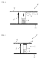
- FIG. 2 is a simplified memory cell 8 that may be a part of a field programmable read-only memory (FPROM) device 10 (see FIG. 8 , too).
- the memory cell 8 may be connected to a word line WL and a bit line BL of the FPROM-device 10.
- FIG. 8 only two bit and word lines BL, WL are depicted for clarity reasons, further word and bit lines WL, BL are denoted by the respective dots in the FPROM-device 10.
- the memory cell 8 of FIG. 2 comprises a top electrode 12 and a bottom electrode 14 that may be connected to a bit line BL and word line WL, respectively.
- a telescoping nanotube 2 is arranged between the top and bottom electrode 12, 14 and provides a switching element for storing bit information.
- FIG. 2 is the non-conductive or opened state of the memory cell 8.
- the switching element i.e. the telescoping element 2 provides no electrical contact between the top and bottom electrode 12, 14. This switching state may be assigned a logical "0".
- An electrical field E between the top and bottom electrode 12, 14 is schematically illustrated by an arrow pointing to the top electrode 12. If the electric field E increases and exceeds a certain threshold, the moveable nanotube 6 is pulled towards the top electrode 12.
- This configuration is illustrated in the further simplified view of FIG. 3 .
- the top and bottom electrode 12, 14 are connected via the telescoping nanotube 2 in this configuration that is referred to as a conductive or closed state of the memory cell 8.
- This state may be assigned a logical "1".
- the electrical connection between the top and bottom electrode is - according to an embodiment of the invention - non-volatile.
- This non-volatility of the electrical connection may be provided by Van-der-Waals forces between an upper and free end 15 of the moveable nanotube 6 and a surface of the top electrode 12 that is facing the free end 15 of the telescoping nanotube 2.
- a mechanical interlock will safeguard the non-volatility of this connection, according to aspects of the invention.
- each storage cell 8 may be configured to be writable only once and to hold the information nearly forever. This one time programmable (OTP) characteristic tailors the memory cell 8 for archiving applications.
- OTP one time programmable
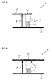
- FIG. 4 is a simplified memory cell 8 comprising a telescoping nanotube 2 having a moveable nanotube 6 that is locked to the top electrode 12.
- An adhesive 16 that is preferably conductive, is deposited onto the free end 15 of the moveable nanotube 6. If the telescoping nanotube 2 is extended by an electrical field E having a suitable strength to cause a sliding of the movable nanotube 6 on the outer surface of the static support nanotube 4, the adhesive 16 will hit the top electrode 12. The moveable nanotube 6 will stick intractably to the top electrode 12.
- the adhesive 16 is glue. Accordingly, the storage cell 8 is locked in its closed state as it is illustrated in FIG. 4 . This may be performed only once and therefore, the storage cell 8 has an OTP characteristic.
- the ON-state of the memory cell 8 may be detected by simply measuring its ohmic resistance. However, even non-conductive adhesives 16 may be applied. In this case, the switching state of the memory cell 8 may be determined by measuring its capacity. The opened and closed state may be distinguished because the capacity of the memory cell 8 is a function of a distance between the free end 15 of the moveable nanotube 6 and the top electrode 12.
- FIG. 5 is a simplified memory cell 8 for an FPROM-device 10 according to another embodiment of the invention.
- the moveable nanotube 6 is mechanically locked to the top electrode 12 by help of an adhesive.
- the adhesive 16 is not deposited on the free end 15 of the moveable nanotube 6 but on the top electrode 12.
- a contact area of the top electrode 12 that is facing the free end 15 of the telescoping nanotube 2 may be coated with a suitable adhesive 16.
- FIG. 6 is another simplified memory cell 8 for an FPROM-device 10, according to another embodiment of the invention.
- a mechanical interlock between the moveable nanotube 6 and the top electrode 12 is provided by applying a two-component adhesive.
- a first chemical agent 18 is deposited onto the free end 15 of the moveable nanotube 6.
- a second chemical agent 20 is deposited onto the contact area of the top electrode 12. If the first and second chemical agent 18, 20 approach each other, a chemical reaction between the two agents may take place. This will fix the moveable nanotube 6 to the top electrode 12. If the reaction product is electrically conductive, the switching state of the memory cell 8 may be determined by measuring its ohmic resistance, again. If the chemical reaction between the first and second agent 18, 20 leads to a non-conductive product, the switching status of the memory cell 8 may be determined by measuring its capacitance.
- the abovementioned embodiments mainly focus on an mechanical interlock between the moveable nanotube 6 and the top electrode 12.
- the following embodiment illustrates a mechanical interlock between the static support nanotube 4 and the moveable nanotube 6.
- the mechanic interlock between the two nanotubes 4, 6 may be realized by applying a variety of different micromechanical locking devices.
- FIG. 7a One embodiment is outlined in FIG. 7a showing a simplified telescoping nanotube 2 having a micromechanical snap-fit element 22.
- This snap-fit element 22 may be a micromechanical snap ring comprising retention arms 23 and a ring surrounding the static support nanotube 4.
- the snap-fit element 22 may be inserted in the annular clearance between the inner surface of the moveable nanotube 6 and the outer surface of the static support nanotube 4. This step is illustrated by the upside down arrow in FIG. 7a .
- the snap-fit element 22 is preloaded or pressurized in this configuration of the telescoping nanotube 2.
- FIG. 7b is a simplified memory cell 8 for an FPROM-device 10, according to another embodiment of the invention.
- the moveable nanotube 6 of the telescoping nanotube 2 may expand. If a bottom edge of the moveable nanotube 6 exceeds the free ends of the lateral retention arms 23 of the snap-fit element 22, these retention arms 23 will expand and fix the moveable nanotube 6 in the first and upper end position. In this configuration, there is an electrical contact between the top electrode 12 and the bottom electrode 14 via the telescoping nanotube 2.
- the telescoping nanotube 2 may be fixed by help of a mechanic interlock between the static support nanotube 4 and the moveable nanotube 6 (e.g. by the snap-fit element 22) and/or by help of mechanically fixing the moveable nanotube 6 to the top electrode 12, as illustrated in the embodiments of FIGs. 4 to 6 .
Landscapes
- Engineering & Computer Science (AREA)
- Chemical & Material Sciences (AREA)
- Nanotechnology (AREA)
- Materials Engineering (AREA)
- Crystallography & Structural Chemistry (AREA)
- Physics & Mathematics (AREA)
- Mathematical Physics (AREA)
- Theoretical Computer Science (AREA)
- Semiconductor Memories (AREA)
Priority Applications (3)
| Application Number | Priority Date | Filing Date | Title |
|---|---|---|---|
| EP11306028A EP2557569A1 (de) | 2011-08-10 | 2011-08-10 | Feldprogrammierbare Festwertspeichervorrichtung |
| US13/551,571 US8923029B2 (en) | 2011-08-10 | 2012-07-17 | Field programmable read-only memory device |
| EP12176638A EP2565876A1 (de) | 2011-08-10 | 2012-07-17 | Feldprogrammierbare Festwertspeichervorrichtung |
Applications Claiming Priority (1)
| Application Number | Priority Date | Filing Date | Title |
|---|---|---|---|
| EP11306028A EP2557569A1 (de) | 2011-08-10 | 2011-08-10 | Feldprogrammierbare Festwertspeichervorrichtung |
Publications (1)
| Publication Number | Publication Date |
|---|---|
| EP2557569A1 true EP2557569A1 (de) | 2013-02-13 |
Family
ID=46489142
Family Applications (2)
| Application Number | Title | Priority Date | Filing Date |
|---|---|---|---|
| EP11306028A Withdrawn EP2557569A1 (de) | 2011-08-10 | 2011-08-10 | Feldprogrammierbare Festwertspeichervorrichtung |
| EP12176638A Withdrawn EP2565876A1 (de) | 2011-08-10 | 2012-07-17 | Feldprogrammierbare Festwertspeichervorrichtung |
Family Applications After (1)
| Application Number | Title | Priority Date | Filing Date |
|---|---|---|---|
| EP12176638A Withdrawn EP2565876A1 (de) | 2011-08-10 | 2012-07-17 | Feldprogrammierbare Festwertspeichervorrichtung |
Country Status (2)
| Country | Link |
|---|---|
| US (1) | US8923029B2 (de) |
| EP (2) | EP2557569A1 (de) |
Families Citing this family (2)
| Publication number | Priority date | Publication date | Assignee | Title |
|---|---|---|---|---|
| EP2363958A1 (de) * | 2010-03-04 | 2011-09-07 | Thomson Licensing | Feldprogrammierbares Gate-Array |
| US10989735B2 (en) * | 2019-08-21 | 2021-04-27 | Facebook Technologies, Llc | Atomic force microscopy tips for interconnection |
Citations (2)
| Publication number | Priority date | Publication date | Assignee | Title |
|---|---|---|---|---|
| US20070171707A1 (en) * | 2006-01-04 | 2007-07-26 | Leonid Maslov | Nonvolatile carbon nanotube memory device using multiwall carbon nanotubes and methods of operating and fabricating the same |
| US20070230241A1 (en) * | 2004-09-30 | 2007-10-04 | California Institute Of Technology | Nanomechanical switching device |
Family Cites Families (9)
| Publication number | Priority date | Publication date | Assignee | Title |
|---|---|---|---|---|
| ES2264928T3 (es) * | 1999-02-12 | 2007-02-01 | Board Of Trustees Operating Michigan State University | Nanocapsulas que contienen particulas cargadas, sus usos y procedimientos de preparacion de las mismas. |
| US20040150472A1 (en) | 2002-10-15 | 2004-08-05 | Rust Thomas F. | Fault tolerant micro-electro mechanical actuators |
| US7456482B2 (en) * | 2004-03-22 | 2008-11-25 | Cabot Microelectronics Corporation | Carbon nanotube-based electronic switch |
| US7394687B2 (en) | 2005-05-09 | 2008-07-01 | Nantero, Inc. | Non-volatile-shadow latch using a nanotube switch |
| KR100723412B1 (ko) | 2005-11-10 | 2007-05-30 | 삼성전자주식회사 | 나노튜브를 이용하는 비휘발성 메모리 소자 |
| KR100651825B1 (ko) | 2005-11-29 | 2006-12-01 | 한국과학기술원 | 기계적인 스위치를 이용한 메모리 어레이, 그의 제어 방법,기계적인 스위치를 이용한 표시 장치 및 그의 제어 방법 |
| KR100745769B1 (ko) * | 2006-09-11 | 2007-08-02 | 삼성전자주식회사 | 나노와이어 전기기계 스위칭 소자 및 그 제조방법, 상기나노와이어 전기기계 소자를 이용한 전기기계 메모리 소자 |
| US20080277718A1 (en) | 2006-11-30 | 2008-11-13 | Mihai Adrian Ionescu | 1T MEMS scalable memory cell |
| US7675768B1 (en) | 2008-08-22 | 2010-03-09 | Fronteon Inc | Low power carbon nanotube memory |
-
2011
- 2011-08-10 EP EP11306028A patent/EP2557569A1/de not_active Withdrawn
-
2012
- 2012-07-17 EP EP12176638A patent/EP2565876A1/de not_active Withdrawn
- 2012-07-17 US US13/551,571 patent/US8923029B2/en not_active Expired - Fee Related
Patent Citations (2)
| Publication number | Priority date | Publication date | Assignee | Title |
|---|---|---|---|---|
| US20070230241A1 (en) * | 2004-09-30 | 2007-10-04 | California Institute Of Technology | Nanomechanical switching device |
| US20070171707A1 (en) * | 2006-01-04 | 2007-07-26 | Leonid Maslov | Nonvolatile carbon nanotube memory device using multiwall carbon nanotubes and methods of operating and fabricating the same |
Non-Patent Citations (2)
| Title |
|---|
| BICHOUTSKAIA E ET AL: "Nanotube-based data storage devices", MATERIALS TODAY, ELSEVIER SCIENCE, KIDLINGTON, GB, vol. 11, no. 6, 1 June 2008 (2008-06-01), pages 38 - 43, XP025711434, ISSN: 1369-7021, [retrieved on 20080601], DOI: 10.1016/S1369-7021(08)70120-2 * |
| JEONG WON KANG ET AL: "Electrostatically telescoping nanotube nonvolatile memory device", NANOTECHNOLOGY, IOP, BRISTOL, GB, vol. 18, no. 9, 7 March 2007 (2007-03-07), pages 95705, XP020119917, ISSN: 0957-4484, DOI: 10.1088/0957-4484/18/9/095705 * |
Also Published As
| Publication number | Publication date |
|---|---|
| US20130039115A1 (en) | 2013-02-14 |
| US8923029B2 (en) | 2014-12-30 |
| EP2565876A1 (de) | 2013-03-06 |
Similar Documents
| Publication | Publication Date | Title |
|---|---|---|
| KR102016399B1 (ko) | 단극 터치 센서 및 그 제조 방법 | |
| US8923029B2 (en) | Field programmable read-only memory device | |
| US6359757B1 (en) | Electrostatic actuator | |
| KR20150022126A (ko) | 가변강성 필름, 가변강성 유연 디스플레이 및 이의 제조 방법 | |
| JP2015181080A (ja) | 気密封止された電子機器用のフィードスルーコネクタ | |
| US9595272B2 (en) | Magnetic media access head with metal coating | |
| JP5052849B2 (ja) | ナノチューブを用いる不揮発性メモリ素子 | |
| US7820311B2 (en) | Ferroelectric recording medium and writing method for the same | |
| US7829886B2 (en) | Nonvolatile carbon nanotube memory device using multiwall carbon nanotubes and methods of operating and fabricating the same | |
| CN109121440B (zh) | 具有小厚度的下壳体的电池组以及包括该电池组的膝上型计算机 | |
| CN104036822B (zh) | 基于基元电容的存储基元和用于操作存储基元的方法 | |
| Singh et al. | Anchor-free NEMS non-volatile memory cell for harsh environment data storage | |
| EP2557568B1 (de) | Programmierbare Festwertspeichervorrichtung und Verfahren zu deren Beschreiben | |
| Ranganathan et al. | Nanomechanical non-volatile memory for computing at extreme | |
| US7626237B1 (en) | Non-volatile MEMS memory cell and method of forming such memory cell | |
| CN106200772A (zh) | 按压结构及具有此按压结构的电子装置 | |
| EP3014624B1 (de) | Anordnung von vertikal ausgerichteten nanoröhrchenarrays mit partikeln und verwendung davon | |
| EP2363871B1 (de) | Elektromechanischer Schalter, Speichervorrichtung mit solch einem elektromechanischen Schalter und Betriebsverfahren dafür | |
| KR100803204B1 (ko) | 디지털 자기저항 센서 | |
| US20070062828A1 (en) | Protective case for data storage disc | |
| US9640927B1 (en) | Jumper assembly | |
| WO2004006258A1 (en) | Disc comprising a substrate having a support plate and a registration layer connected to the support plate | |
| JP5883460B2 (ja) | ディスク保持体の設けられた2枚ディスクトレイ | |
| CN201662989U (zh) | Usb随身碟的结构 | |
| US20190279677A1 (en) | Disk clamping mechanism including annular ring member |
Legal Events
| Date | Code | Title | Description |
|---|---|---|---|
| PUAI | Public reference made under article 153(3) epc to a published international application that has entered the european phase |
Free format text: ORIGINAL CODE: 0009012 |
|
| AK | Designated contracting states |
Kind code of ref document: A1 Designated state(s): AL AT BE BG CH CY CZ DE DK EE ES FI FR GB GR HR HU IE IS IT LI LT LU LV MC MK MT NL NO PL PT RO RS SE SI SK SM TR |
|
| AX | Request for extension of the european patent |
Extension state: BA ME |
|
| STAA | Information on the status of an ep patent application or granted ep patent |
Free format text: STATUS: THE APPLICATION IS DEEMED TO BE WITHDRAWN |
|
| 18D | Application deemed to be withdrawn |
Effective date: 20130814 |