EP2557632A1 - Structure de connexion de câble - Google Patents
Structure de connexion de câble Download PDFInfo
- Publication number
- EP2557632A1 EP2557632A1 EP11765403A EP11765403A EP2557632A1 EP 2557632 A1 EP2557632 A1 EP 2557632A1 EP 11765403 A EP11765403 A EP 11765403A EP 11765403 A EP11765403 A EP 11765403A EP 2557632 A1 EP2557632 A1 EP 2557632A1
- Authority
- EP
- European Patent Office
- Prior art keywords
- flat section
- substrate
- connection structure
- cable
- cable connection
- Prior art date
- Legal status (The legal status is an assumption and is not a legal conclusion. Google has not performed a legal analysis and makes no representation as to the accuracy of the status listed.)
- Granted
Links
Images


Classifications
-
- H—ELECTRICITY
- H01—ELECTRIC ELEMENTS
- H01R—ELECTRICALLY-CONDUCTIVE CONNECTIONS; STRUCTURAL ASSOCIATIONS OF A PLURALITY OF MUTUALLY-INSULATED ELECTRICAL CONNECTING ELEMENTS; COUPLING DEVICES; CURRENT COLLECTORS
- H01R9/00—Structural associations of a plurality of mutually-insulated electrical connecting elements, e.g. terminal strips or terminal blocks; Terminals or binding posts mounted upon a base or in a case; Bases therefor
- H01R9/03—Connectors arranged to contact a plurality of the conductors of a multiconductor cable, e.g. tapping connections
- H01R9/05—Connectors arranged to contact a plurality of the conductors of a multiconductor cable, e.g. tapping connections for coaxial cables
- H01R9/0515—Connection to a rigid planar substrate, e.g. printed circuit board
-
- H—ELECTRICITY
- H01—ELECTRIC ELEMENTS
- H01R—ELECTRICALLY-CONDUCTIVE CONNECTIONS; STRUCTURAL ASSOCIATIONS OF A PLURALITY OF MUTUALLY-INSULATED ELECTRICAL CONNECTING ELEMENTS; COUPLING DEVICES; CURRENT COLLECTORS
- H01R4/00—Electrically-conductive connections between two or more conductive members in direct contact, i.e. touching one another; Means for effecting or maintaining such contact; Electrically-conductive connections having two or more spaced connecting locations for conductors and using contact members penetrating insulation
- H01R4/02—Soldered or welded connections
Definitions
- the present invention relates to a cable connection structure in which a coaxial cable is connected to a substrate.
- a structure for connecting a coaxial cable As a structure for connecting a coaxial cable, a structure in which a slit is provided on an upper surface of a printed circuit substrate and a pattern for connection with an external conductor is formed at both sides of the slit has been known as disclosed in Japanese Patent Application Laid-Open No. 2001-68175 . According to the technique disclosed in Japanese Patent Application Laid-Open No. 2001-68175 , the external conductor of the coaxial cable is placed in the slit provided in the printed circuit substrate and can be connected to the pattern for connection at both sides of the slit, so that it is possible to make a height of an attachment of the coaxial cable low by a portion by which the external conductor drops in the slit.
- a cable connection structure includes a cable that has an outer skin and at least one conducting wire, and a substrate to which the cable is connected at a main surface side having a hard wiring, wherein the substrate includes, at the main surface side, a first flat section having flatness and a second flat section having flatness thinner than the first flat section via a level difference surface from the first flat section and an end part of the outer skin is arranged on the second flat section and at least one of the conducting wire is connected to a connecting electrode formed on the second flat section.
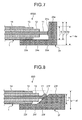
- FIG. 1 is a partial cross sectional view of a cable connection structure 100 according to a first embodiment.
- FIG. 2 is a perspective view of a configuration of a substrate 2 to which a coaxial cable 1 is connected by the cable connection structure 100 according to the first embodiment.
- the cable connection structure 100 is provided with the coaxial cable 1 and the substrate 2 to which the coaxial cable 1 is connected as shown in FIG. 1 .
- the coaxial cable 1 is provided with a center conductor 11 as a core wire, an internal insulator 12 provided in an outer circumference of the center conductor 11, an external conductor 13 as a shielding wire that covers an outer circumference of the internal insulator 12, and an outer insulator 14 provided in an outer circumference of the external conductor 13.
- the substrate 2 is provided with a first flat section 23 having flatness and a second flat section 24 that has a surface flush with the first flat section 23 and has flatness whose thickness is less than that of the first flat section 23 as shown in FIG. 2 .
- a level difference surface 25 formed in a boundary between the first flat section 23 and the second flat section 24 is formed perpendicularly to a main surface of the first flat section 23 and a main surface of the second flat section 24. In other words, the first flat section 23 and the second flat section 24 are formed via the level difference surface 25.
- a center conductor connecting electrode 21 to which an end part of the center conductor 11 is connected is formed on the main surface of the first flat section 23 and an external conductor connecting electrode 22 to which an end part of the external conductor 13 is connected is formed on the main surface of the second flat section 24.
- the level difference surface 25 of the substrate 2 is formed by performing a process such as an etching only on a predetermined area of a predetermined surface of the substrate 2. After forming the level difference surface 25, the external conductor connecting electrode 22 is formed on the main surface of the second flat section 24 and the center conductor connecting electrode 21 is formed on the main surface of the first flat section 23. In the case of forming the level difference surface 25 by etching and the like, a silicon substrate is preferably used.
- a ceramic substrate and the like may be applied and the level difference surface 25 in a ceramic substrate is formed by laminating ceramic layers only at a predetermined area of a predetermined surface of the substrate 2.
- the end part of the center conductor 11 of the coaxial cable 1 and the center conductor connecting electrode 21, and the end part of the external conductor 13 and the external conductor connecting electrode 22 are electrically and mechanically connected by using a conductive bonding member, not shown, such as a solder, an anisotropically-conductive film (ACF), and an anisotropically-conductive paste (ACP).
- a conductive bonding member not shown, such as a solder, an anisotropically-conductive film (ACF), and an anisotropically-conductive paste (ACP).
- the coaxial cable 1 and the substrate 2 are connected by arranging the conductive bonding member such as a solder, bonding the end part of the center conductor 11 of the coaxial cable 1 and the center conductor connecting electrode 21 formed on the main surface of the first flat section 23 of the substrate 2, and bonding the end part of the external conductor 13 and the external conductor connecting electrode 22 formed on the main surface of the flat section 24 in the cable connection structure 100 according to the first embodiment.
- the conductive bonding member such as a solder
- the cable connection structure 100 can be applied to a connection between an ultrasonic transducer of an ultrasonic endoscope and a coaxial cable, for example.
- FIG. 3 is a partial cross sectional view of a cable connection structure 200 according to a second embodiment.
- the same part as the first embodiment is assigned with the same reference symbol.
- a center conductor connecting electrode 21b of a substrate 2b is formed on a main surface of a second flat section 24b in the cable connection structure 200 according to the second embodiment.
- the coaxial cable 1 and the substrate 2b are electrically and mechanically connected by a conductive bonding member, not shown, such as a solder and an ACF similarly to the first embodiment.
- a conductive bonding member such as a solder and an ACF similarly to the first embodiment.
- the end part of the center conductor 11 of the coaxial cable 1 and the center conductor connecting electrode 21b, and the end part of the external conductor 13 and an external conductor connecting electrode 22b are electrically and mechanically connected by a conductive bonding member, not shown, such as a solder, an ACF, and an ACP.
- the cable connection structure 200 according to the second embodiment it is possible in the cable connection structure 200 according to the second embodiment to obtain the same effect as the first embodiment. Besides, since the center conductor connecting electrode 21b of the substrate 2b is formed on the main surface of the second flat section 24b, it is possible to connect the coaxial cable 1 to the substrate 2b by using a general cable connection method of connecting a cable to a flat substrate surface.
- the cable connection structure 200 can be applied to a connection between an ultrasonic transducer of an ultrasonic endoscope and a coaxial cable, for example.
- FIG. 4 is a partial cross sectional view of a cable connection structure 300 according to a third embodiment.
- the same part as the first and the second embodiments is assigned with the same reference symbol.
- a level difference surface 25c between a first flat section 23c and a second flat section 24c of a substrate 2c has a height equal to or more than a radius of the coaxial cable 1 in the cable connection structure 300 according to the third embodiment.
- the coaxial cable 1 and the substrate 2c are electrically and mechanically connected by a conductive bonding member, not shown, such as a solder and an ACF similarly to the first and the second embodiments.
- a conductive bonding member such as a solder and an ACF similarly to the first and the second embodiments.
- the end part of the center conductor 11 of the coaxial cable 1 and a center conductor connecting electrode 21c, and the end part of the external conductor 13 and an external conductor connecting electrode 22c are electrically and mechanically connected by a conductive bonding member, not shown, such as a solder, an ACF, and an ACP.
- a height 7c of the level difference surface 25c between the first flat section 23c and the second flat section 24c of the substrate 2c is configured to be equal to or more than a radius 8 of the coaxial cable 1, it is possible to reduce a height 4c of the attachment part of the coaxial cable 1 to the substrate 2c by not less than the radius 8 of the coaxial cable 1.
- the cable connection structure 300 according to the third embodiment it is possible in the cable connection structure 300 according to the third embodiment to obtain the same advantageous effects as the first and the second embodiments.
- the cable connection structure 300 can be applied to a connection between an ultrasonic transducer of an ultrasonic endoscope and a coaxial cable, for example.
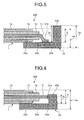
- FIG. 5 is a partial cross sectional view of a cable connection structure 400 according to a fourth embodiment.
- the same part as the first to the third embodiments is assigned with the same reference symbol.
- a height 7d of a level difference surface 25d between a first flat section 23d and a second flat section 24d of a substrate 2d is equal to or more than the diameter 6 of the coaxial cable 1 in the cable connection structure 400 according to the fourth embodiment.
- the coaxial cable 1 and the substrate 2d are electrically and mechanically connected by a conductive bonding member, not shown, such as a solder and an ACF similarly to the first to the third embodiments.
- a conductive bonding member such as a solder and an ACF similarly to the first to the third embodiments.
- the end part of the center conductor 11 of the coaxial cable 1 and a center conductor connecting electrode 21d, and the end part of the external conductor 13 and an external conductor connecting electrode 22d are electrically and mechanically connected by a conductive bonding member, not shown, such as a solder, an ACF, and an ACP.
- the cable connection structure 400 according to the fourth embodiment it is possible in the cable connection structure 400 according to the fourth embodiment to obtain the same effect as the first to the third embodiments.
- the height 7d of the level difference surface 25d between the first flat section 23d and the second flat section 24d of the substrate 2d is configured to be equal to or more than the diameter 6 of the coaxial cable 1, it is possible to suppress a height 4d of the attachment part of the coaxial cable 1 to the substrate 2d to such a degree as to be not more than a thickness 5d of the first flat section 23d of the substrate 2d.
- the cable connection structure 400 according to the fourth embodiment can obtain the same advantageous effects as the first to the third embodiments.
- the height 7d of the level difference surface 25d of the substrate 2d is configured to be not less than the diameter 6 of the coaxial cable 1
- the cable connection structure 400 can be applied to a connection between an ultrasonic transducer of an ultrasonic endoscope and a coaxial cable, for example.
- FIG. 6 is a partial cross sectional view of a cable connection structure 500 according to a fifth embodiment.
- the same part as the first to the fourth embodiments is assigned with the same reference symbol.
- the cable connection structure 500 according to the fifth embodiment is configured such that a height 7e of a level difference surface 25e between a first flat section 23e and a second flat section 24e of a substrate 2e is equal to or less than the diameter 6 of the coaxial cable 1.
- a center conductor connecting electrode 21e is formed on the level difference surface 25e (vertical surface) of the substrate 2e in the coaxial cable connection structure 500 according to the fifth embodiment.
- the coaxial cable 1 and the substrate 2e are electrically and mechanically connected by a conductive bonding member, not shown, such as a solder and an ACF similarly to the first to the fourth embodiments.
- a conductive bonding member such as a solder and an ACF similarly to the first to the fourth embodiments.
- the end part of the center conductor 11 of the coaxial cable 1 and the center conductor connecting electrode 21e, and the end part of the external conductor 13 and an external conductor connecting electrode 22e are electrically and mechanically connected by a conductive bonding member, not shown, such as a solder, an ACF, and an ACP.
- the cable connection structure 500 according to the fifth embodiment it is possible in the cable connection structure 500 according to the fifth embodiment to obtain the same effect as the first embodiment. Specifically, it is possible to reduce a height 4e of the attachment part of the coaxial cable 1 by the height 7e of the level difference surface 25e. In addition, there becomes no necessity of forming the center conductor connecting electrode 21e on a main surface of the first flat section 23e and a main surface of the second flat section 24e.
- the cable connection structure 500 it is possible in the cable connection structure 500 according to the fifth embodiment to obtain the same advantageous effects as the first embodiment.
- the cable connection structure 500 can be applied to a connection between an ultrasonic transducer of an ultrasonic endoscope and a coaxial cable, for example.
- FIG. 7 is a partial cross sectional view explaining the cable connection structure 500A according to the modification of the fifth embodiment.
- the center conductor connecting electrode 21e is formed on the level difference surface 25e (vertical surface) of the substrate 2e in the cable connection structure 500A according to the first modification of the fifth embodiment.
- the height 4e of the attachment part of the coaxial cable 1 to the substrate 2e less than a thickness 5e of the first flat section 23e of the substrate 2e and to connect the coaxial cable 1 to the substrate 2e without causing an increase in the height 4e of the attachment part.
- FIG. 8 is a partial cross sectional view of a cable connection structure 600 according to a sixth embodiment.
- the same part as the first to the fifth embodiments is assigned with the same reference symbol.
- the cable connection structure 600 according to the sixth embodiment is configured such that a height 7f of a level difference surface 25f between a first flat section 23f and a second flat section 24f of a substrate 2f is equal to or less than the diameter of the coaxial cable 1. As shown in FIG.
- the level difference surface 25f between the first flat section 23f and the second flat section 24f of the substrate 2f is formed as a slope surface not perpendicular to main surfaces of the first flat section 23f and the second flat section 24f in the cable connection structure 600 according to the sixth embodiment.
- the substrate 2f is assumed to be a silicon substrate and the level difference surface 25f is obtained as a slope surface by a process through an anisotropic etching of a predetermined side surface of the substrate 2f, for example.
- an external conductor connecting electrode 22f is formed on the main surface of the second flat section 24f and a center conductor connecting electrode 21f is formed on the level difference surface 25f as a slope surface.
- the substrate 2f is not limited to the case of being constituted by a silicon substrate, and a ceramic substrate and the like may be similarly applied.
- a ceramic substrate is used for the substrate 2f, an electrode can be formed on the level difference surface 25f as a slope surface by laminating ceramic layers in which electrode layers are formed at an edge part.
- the coaxial cable 1 and the substrate 2f are electrically and mechanically connected by a conductive bonding member, not shown, such as a solder and an ACF similarly to the first to the fifth embodiments.
- a conductive bonding member such as a solder and an ACF similarly to the first to the fifth embodiments.
- the end part of the center conductor 11 of the coaxial cable 1 and the center conductor connecting electrode 21f, and the end part of the external conductor 13 and the external conductor connecting electrode 22f are electrically and mechanically connected by a conductive bonding member, not shown, such as a solder, an ACF, and an ACP.
- the cable connection structure 600 according to the sixth embodiment it is possible in the cable connection structure 600 according to the sixth embodiment to obtain the same effect as the first embodiment. Specifically, it is possible to reduce a height 4f of the attachment part of the coaxial cable 1 by the height 7f of the level difference surface 25f. Therefore, it is possible to suppress an increase, associated with the connection of the coaxial cable 1, in the direction of the thickness of the substrate 2f.
- the level difference surface 25f of the substrate 2f is configured not to be perpendicular but to be a slope surface and the center conductor connecting electrode 21f is arranged on the level difference surface 25f, it is possible to make a projection area of the center conductor connecting electrode 21f in the direction perpendicular to the main surface of the first flat section 23f and the main surface of the second flat section 24f small without making a connection area between the center conductor connecting electrode 21f and the end part of the center conductor 11 small.
- the cable connection structure 600 can be applied to a connection between an ultrasonic transducer of an ultrasonic endoscope and a coaxial cable, for example.
- a distal end part of the center conductor 11 may be formed to have a slope surface whose inclination is substantially the same as that of the level difference surface 25f and the slope surface formed at the distal end of the center conductor 11 and the center conductor connecting electrode 21f on the level difference surface 25f may be connected by a conductive film and the like to connect the center conductor 11 and the center conductor connecting electrode 21f.
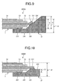
- FIG. 9 is a partial cross sectional view of a cable connection structure 600A according to the first modification of the sixth embodiment.
- the center conductor connecting electrode 21f is formed on the level difference surface 25f as a slope surface in the cable connection structure 600A according to the first modification of the sixth embodiment.
- the height 4f of the attachment part of the coaxial cable 1 to the substrate 2f less than the thickness of the first flat section 23f of the substrate 2f and to connect the coaxial cable 1 to the substrate 2f without causing an increase in the height 4f of the attachment part since the height 7f of the level difference surface 25f is made more than the diameter 6 of the coaxial cable 1.
- the level difference surface 25f of the substrate 2f is configured to be a slope surface which is not perpendicular to the main surfaces of the first flat section 23f and the second flat section 24f of the substrate 2f and the center conductor connecting electrode 21f is arranged on the level difference surface 25f, it is possible to make a projection area of the center conductor connecting electrode 21f in the direction perpendicular to the main surface of the first flat section 23f and the main surface of the second flat section 24f small without making a connection area of the end part of the center conductor 11 to the center conductor connecting electrode 21f small.
- FIG. 10 is a partial cross sectional view of a cable connection structure 600B according to the second modification of the sixth embodiment.
- the level difference surface 25f between the first flat section 23f and the second flat section 24f of the substrate 2f is formed as a slope surface with respect to the main surfaces of the first flat section 23f and the second flat section 24f in the cable connection structure 600B according to the second modification of the sixth embodiment.
- the present invention is not limited to the embodiments and may be applied to a cable of other kinds except for the coaxial cable, for example, a cable in which one or more conducting wire is covered by an outer skin.
- a cable in which one or more conducting wire is covered by an outer skin for example, a cable in which one or more conducting wire is covered by an outer skin.
- by connecting at least one conducting wire to the second flat section as a thinner part of the substrate or the level difference surface it is possible to connect the cable to the substrate with a reduction in height of the cable attachment part.
- a height of an attachment part of the cable to the substrate can be reduced by a height of the level difference surface formed in the substrate, or the cable can be connected to the substrate without causing an increase in height of the attachment part when the height of the level difference surface is more than a diameter of the cable.
Landscapes
- Coupling Device And Connection With Printed Circuit (AREA)
- Multi-Conductor Connections (AREA)
Applications Claiming Priority (2)
| Application Number | Priority Date | Filing Date | Title |
|---|---|---|---|
| JP2010089788A JP5631618B2 (ja) | 2010-04-08 | 2010-04-08 | ケーブル接続構造 |
| PCT/JP2011/057030 WO2011125502A1 (fr) | 2010-04-08 | 2011-03-23 | Structure de connexion de câble |
Publications (3)
| Publication Number | Publication Date |
|---|---|
| EP2557632A1 true EP2557632A1 (fr) | 2013-02-13 |
| EP2557632A4 EP2557632A4 (fr) | 2014-05-21 |
| EP2557632B1 EP2557632B1 (fr) | 2017-01-11 |
Family
ID=44762456
Family Applications (1)
| Application Number | Title | Priority Date | Filing Date |
|---|---|---|---|
| EP11765403.8A Not-in-force EP2557632B1 (fr) | 2010-04-08 | 2011-03-23 | Structure de connexion de câble |
Country Status (5)
| Country | Link |
|---|---|
| US (1) | US9356365B2 (fr) |
| EP (1) | EP2557632B1 (fr) |
| JP (1) | JP5631618B2 (fr) |
| CN (1) | CN102804507B (fr) |
| WO (1) | WO2011125502A1 (fr) |
Families Citing this family (16)
| Publication number | Priority date | Publication date | Assignee | Title |
|---|---|---|---|---|
| WO2014199897A1 (fr) | 2013-06-10 | 2014-12-18 | オリンパス株式会社 | Structure de connexion de câble |
| CN106105407A (zh) * | 2014-03-20 | 2016-11-09 | 奥林巴斯株式会社 | 缆线连接构造和内窥镜装置 |
| CN106663496B (zh) * | 2014-05-16 | 2019-05-17 | 住友电气工业株式会社 | 多芯电缆和具有基板的多芯电缆 |
| CN204143896U (zh) * | 2014-09-12 | 2015-02-04 | 富士康(昆山)电脑接插件有限公司 | 线缆连接器组件 |
| JPWO2017081720A1 (ja) * | 2015-11-09 | 2018-08-30 | オリンパス株式会社 | ケーブル接続構造、撮像モジュールおよび内視鏡 |
| JP6519462B2 (ja) * | 2015-12-10 | 2019-05-29 | 住友電気工業株式会社 | ケーブルアセンブリ |
| TWM531078U (zh) * | 2015-12-31 | 2016-10-21 | Zhi-Shou Wang | 電連接器 |
| WO2017122335A1 (fr) * | 2016-01-14 | 2017-07-20 | オリンパス株式会社 | Dispositif d'imagerie, endoscope, et procédé de production de dispositif d'imagerie |
| DE112016006804T5 (de) | 2016-04-28 | 2019-01-24 | Olympus Corporation | Kabelverbindungsstruktur, Bildgebungsvorrichtung und Endoskop |
| JP6393018B1 (ja) * | 2017-04-06 | 2018-09-19 | オリンパス株式会社 | 撮像ユニット、および内視鏡 |
| WO2018186163A1 (fr) * | 2017-04-06 | 2018-10-11 | オリンパス株式会社 | Unité d'imagerie et endoscope |
| CN110545614B (zh) * | 2018-05-29 | 2021-04-20 | 上海华为技术有限公司 | 印刷电路板传输带线以及电子设备 |
| DE102018115651A1 (de) | 2018-06-28 | 2020-01-02 | Peiker Acustic Gmbh | Verfahren zur Herstellung einer Kabelverbindungsstruktur, Kabelverbindungsstruktur und Mikrofonanordnung |
| WO2020012566A1 (fr) * | 2018-07-10 | 2020-01-16 | オリンパス株式会社 | Structure de connexion de câbles, endoscope et procédé de fabrication de structure de connexion de câbles |
| WO2020079736A1 (fr) * | 2018-10-15 | 2020-04-23 | オリンパス株式会社 | Structure de connexion de câble, endoscope et procédé de fabrication de structure de connexion de câble |
| JP7740060B2 (ja) * | 2022-02-24 | 2025-09-17 | 住友電気工業株式会社 | 接続体 |
Family Cites Families (19)
| Publication number | Priority date | Publication date | Assignee | Title |
|---|---|---|---|---|
| JPH07115712B2 (ja) | 1987-11-24 | 1995-12-13 | 吉昌 田原 | 容器の起立回転式の開き蓋 |
| JPH01139365U (fr) * | 1988-03-16 | 1989-09-22 | ||
| JPH09252167A (ja) * | 1996-03-15 | 1997-09-22 | Fujitsu Ltd | 基 板 |
| JP2000068175A (ja) | 1998-08-24 | 2000-03-03 | Advanced Display Inc | 発塵検出方法と、液晶表示装置または半導体装置の製造方法 |
| JPH11352413A (ja) * | 1999-04-27 | 1999-12-24 | Olympus Optical Co Ltd | 内視鏡 |
| JP2001054194A (ja) * | 1999-08-05 | 2001-02-23 | Olympus Optical Co Ltd | アセンブリ基板 |
| JP4151168B2 (ja) | 1999-08-30 | 2008-09-17 | ミツミ電機株式会社 | アンテナ装置 |
| JP3976473B2 (ja) | 2000-05-09 | 2007-09-19 | 日本電気株式会社 | 高周波回路及びそれを用いたモジュール、通信機 |
| JP2003338693A (ja) | 2002-05-20 | 2003-11-28 | Tdk Corp | 同軸ケーブルの接続方法及び多層プリント基板 |
| US6857898B2 (en) * | 2002-07-25 | 2005-02-22 | Tektronix, Inc. | Apparatus and method for low-profile mounting of a multi-conductor coaxial cable launch to an electronic circuit board |
| DE102004060416B4 (de) * | 2004-12-14 | 2007-06-14 | Endress + Hauser Flowtec Ag | Verfahren zur Befestigung eines Koaxialkabels an einer Leiterplatte und entsprechende Leiterplatte |
| US20090090452A1 (en) * | 2005-06-29 | 2009-04-09 | Kabushiki Kaisha Toshiba | Process for producing nonflat ceramic substrate |
| JP4935053B2 (ja) * | 2005-11-09 | 2012-05-23 | 住友電気工業株式会社 | 多心ケーブルの接続構造及び多心ケーブル接続構造体の製造方法 |
| US7498523B2 (en) * | 2006-02-06 | 2009-03-03 | Efficere Inc. | Direct wire attach |
| JP2007265770A (ja) | 2006-03-28 | 2007-10-11 | Sumitomo Electric Ind Ltd | 導体接続構造、および導体接続方法 |
| JP5041925B2 (ja) * | 2007-08-31 | 2012-10-03 | オリンパスメディカルシステムズ株式会社 | 撮像ユニット |
| JP2009081009A (ja) * | 2007-09-26 | 2009-04-16 | Sumitomo Electric Ind Ltd | 極細同軸ハーネス,配線板接続体,配線板モジュールおよび電子機器 |
| JP5163865B2 (ja) | 2007-11-14 | 2013-03-13 | 日立電線株式会社 | 多芯ケーブルアセンブリ及びその製造方法 |
| JP5420389B2 (ja) * | 2009-12-24 | 2014-02-19 | オリンパス株式会社 | ケーブル接続構造 |
-
2010
- 2010-04-08 JP JP2010089788A patent/JP5631618B2/ja active Active
-
2011
- 2011-03-23 WO PCT/JP2011/057030 patent/WO2011125502A1/fr not_active Ceased
- 2011-03-23 CN CN201180014747.7A patent/CN102804507B/zh not_active Expired - Fee Related
- 2011-03-23 EP EP11765403.8A patent/EP2557632B1/fr not_active Not-in-force
-
2012
- 2012-09-13 US US13/613,912 patent/US9356365B2/en active Active
Also Published As
| Publication number | Publication date |
|---|---|
| WO2011125502A1 (fr) | 2011-10-13 |
| JP5631618B2 (ja) | 2014-11-26 |
| EP2557632A4 (fr) | 2014-05-21 |
| CN102804507A (zh) | 2012-11-28 |
| CN102804507B (zh) | 2016-08-10 |
| EP2557632B1 (fr) | 2017-01-11 |
| US20130005181A1 (en) | 2013-01-03 |
| JP2011222277A (ja) | 2011-11-04 |
| US9356365B2 (en) | 2016-05-31 |
Similar Documents
| Publication | Publication Date | Title |
|---|---|---|
| EP2557632A1 (fr) | Structure de connexion de câble | |
| JP4364265B2 (ja) | コネクタ及びそれを備えた電子機器 | |
| JP5657217B2 (ja) | 集合ケーブル | |
| JP5583372B2 (ja) | 集合ケーブル、電子回路モジュールおよび撮像装置 | |
| EP2913897B1 (fr) | Structure de connecteur, connecteur femelle et connecteur mâle | |
| CN102301842A (zh) | 印刷电路组件 | |
| CN105409144A (zh) | 高频超声探头 | |
| JP6008603B2 (ja) | 半導体装置 | |
| US10128588B2 (en) | Cable connecting structure | |
| JP2008210563A (ja) | 多心同軸ケーブルおよび多心同軸ケーブルの製造方法 | |
| JP6118924B1 (ja) | MicroUSBコネクタ | |
| JP2008258053A (ja) | ワイヤケーブルの端末接合構造 | |
| TWI276262B (en) | Connector adapted to be used for transmission of a balanced signal and substrate for mounting the connector | |
| JP2008186719A (ja) | ハーネス、コネクタ付ハーネス、およびハーネス接続体 | |
| JP2007200747A (ja) | 特性インピーダンスの整合が可能なシールドフレキシブルフラットケーブル | |
| CN112806105B (zh) | 电路基板以及具备该电路基板的电缆束 | |
| CN114496358A (zh) | 一种连接线结构及其形成方法 | |
| JP6400985B2 (ja) | 電子素子実装用基板及び電子装置 | |
| JP5702192B2 (ja) | フローティングコネクタ | |
| CN102769234B (zh) | 连接器 | |
| CN111585138B (zh) | 电缆和制造电缆的方法 | |
| JP2007329327A (ja) | 半導体装置及びその製造方法 | |
| JP2006061327A (ja) | 電子内視鏡の先端部 | |
| CN112770478A (zh) | 电子基板以及电子基板的制造方法 | |
| JP2001156202A (ja) | セラミック多層基板 |
Legal Events
| Date | Code | Title | Description |
|---|---|---|---|
| PUAI | Public reference made under article 153(3) epc to a published international application that has entered the european phase |
Free format text: ORIGINAL CODE: 0009012 |
|
| 17P | Request for examination filed |
Effective date: 20121004 |
|
| AK | Designated contracting states |
Kind code of ref document: A1 Designated state(s): AL AT BE BG CH CY CZ DE DK EE ES FI FR GB GR HR HU IE IS IT LI LT LU LV MC MK MT NL NO PL PT RO RS SE SI SK SM TR |
|
| DAX | Request for extension of the european patent (deleted) | ||
| A4 | Supplementary search report drawn up and despatched |
Effective date: 20140417 |
|
| RIC1 | Information provided on ipc code assigned before grant |
Ipc: H01R 9/05 20060101AFI20140411BHEP Ipc: H01R 4/02 20060101ALN20140411BHEP |
|
| 17Q | First examination report despatched |
Effective date: 20150413 |
|
| GRAP | Despatch of communication of intention to grant a patent |
Free format text: ORIGINAL CODE: EPIDOSNIGR1 |
|
| RIC1 | Information provided on ipc code assigned before grant |
Ipc: H01R 4/02 20060101ALN20160705BHEP Ipc: H01R 9/05 20060101AFI20160705BHEP |
|
| RIC1 | Information provided on ipc code assigned before grant |
Ipc: H01R 9/05 20060101AFI20160712BHEP Ipc: H01R 4/02 20060101ALN20160712BHEP |
|
| INTG | Intention to grant announced |
Effective date: 20160727 |
|
| GRAS | Grant fee paid |
Free format text: ORIGINAL CODE: EPIDOSNIGR3 |
|
| GRAA | (expected) grant |
Free format text: ORIGINAL CODE: 0009210 |
|
| RAP1 | Party data changed (applicant data changed or rights of an application transferred) |
Owner name: OLYMPUS CORPORATION |
|
| AK | Designated contracting states |
Kind code of ref document: B1 Designated state(s): AL AT BE BG CH CY CZ DE DK EE ES FI FR GB GR HR HU IE IS IT LI LT LU LV MC MK MT NL NO PL PT RO RS SE SI SK SM TR |
|
| REG | Reference to a national code |
Ref country code: GB Ref legal event code: FG4D |
|
| RIN1 | Information on inventor provided before grant (corrected) |
Inventor name: YAMADA, JUNYA Inventor name: NAKAMURA, MIKIO |
|
| REG | Reference to a national code |
Ref country code: CH Ref legal event code: EP |
|
| REG | Reference to a national code |
Ref country code: AT Ref legal event code: REF Ref document number: 862062 Country of ref document: AT Kind code of ref document: T Effective date: 20170115 |
|
| REG | Reference to a national code |
Ref country code: IE Ref legal event code: FG4D |
|
| REG | Reference to a national code |
Ref country code: DE Ref legal event code: R096 Ref document number: 602011034289 Country of ref document: DE |
|
| REG | Reference to a national code |
Ref country code: LT Ref legal event code: MG4D |
|
| REG | Reference to a national code |
Ref country code: NL Ref legal event code: MP Effective date: 20170111 |
|
| REG | Reference to a national code |
Ref country code: AT Ref legal event code: MK05 Ref document number: 862062 Country of ref document: AT Kind code of ref document: T Effective date: 20170111 |
|
| PG25 | Lapsed in a contracting state [announced via postgrant information from national office to epo] |
Ref country code: NL Free format text: LAPSE BECAUSE OF FAILURE TO SUBMIT A TRANSLATION OF THE DESCRIPTION OR TO PAY THE FEE WITHIN THE PRESCRIBED TIME-LIMIT Effective date: 20170111 |
|
| PG25 | Lapsed in a contracting state [announced via postgrant information from national office to epo] |
Ref country code: HR Free format text: LAPSE BECAUSE OF FAILURE TO SUBMIT A TRANSLATION OF THE DESCRIPTION OR TO PAY THE FEE WITHIN THE PRESCRIBED TIME-LIMIT Effective date: 20170111 Ref country code: IS Free format text: LAPSE BECAUSE OF FAILURE TO SUBMIT A TRANSLATION OF THE DESCRIPTION OR TO PAY THE FEE WITHIN THE PRESCRIBED TIME-LIMIT Effective date: 20170511 Ref country code: LT Free format text: LAPSE BECAUSE OF FAILURE TO SUBMIT A TRANSLATION OF THE DESCRIPTION OR TO PAY THE FEE WITHIN THE PRESCRIBED TIME-LIMIT Effective date: 20170111 Ref country code: NO Free format text: LAPSE BECAUSE OF FAILURE TO SUBMIT A TRANSLATION OF THE DESCRIPTION OR TO PAY THE FEE WITHIN THE PRESCRIBED TIME-LIMIT Effective date: 20170411 Ref country code: FI Free format text: LAPSE BECAUSE OF FAILURE TO SUBMIT A TRANSLATION OF THE DESCRIPTION OR TO PAY THE FEE WITHIN THE PRESCRIBED TIME-LIMIT Effective date: 20170111 Ref country code: GR Free format text: LAPSE BECAUSE OF FAILURE TO SUBMIT A TRANSLATION OF THE DESCRIPTION OR TO PAY THE FEE WITHIN THE PRESCRIBED TIME-LIMIT Effective date: 20170412 |
|
| PG25 | Lapsed in a contracting state [announced via postgrant information from national office to epo] |
Ref country code: BG Free format text: LAPSE BECAUSE OF FAILURE TO SUBMIT A TRANSLATION OF THE DESCRIPTION OR TO PAY THE FEE WITHIN THE PRESCRIBED TIME-LIMIT Effective date: 20170411 Ref country code: SE Free format text: LAPSE BECAUSE OF FAILURE TO SUBMIT A TRANSLATION OF THE DESCRIPTION OR TO PAY THE FEE WITHIN THE PRESCRIBED TIME-LIMIT Effective date: 20170111 Ref country code: AT Free format text: LAPSE BECAUSE OF FAILURE TO SUBMIT A TRANSLATION OF THE DESCRIPTION OR TO PAY THE FEE WITHIN THE PRESCRIBED TIME-LIMIT Effective date: 20170111 Ref country code: LV Free format text: LAPSE BECAUSE OF FAILURE TO SUBMIT A TRANSLATION OF THE DESCRIPTION OR TO PAY THE FEE WITHIN THE PRESCRIBED TIME-LIMIT Effective date: 20170111 Ref country code: ES Free format text: LAPSE BECAUSE OF FAILURE TO SUBMIT A TRANSLATION OF THE DESCRIPTION OR TO PAY THE FEE WITHIN THE PRESCRIBED TIME-LIMIT Effective date: 20170111 Ref country code: PT Free format text: LAPSE BECAUSE OF FAILURE TO SUBMIT A TRANSLATION OF THE DESCRIPTION OR TO PAY THE FEE WITHIN THE PRESCRIBED TIME-LIMIT Effective date: 20170511 Ref country code: PL Free format text: LAPSE BECAUSE OF FAILURE TO SUBMIT A TRANSLATION OF THE DESCRIPTION OR TO PAY THE FEE WITHIN THE PRESCRIBED TIME-LIMIT Effective date: 20170111 Ref country code: RS Free format text: LAPSE BECAUSE OF FAILURE TO SUBMIT A TRANSLATION OF THE DESCRIPTION OR TO PAY THE FEE WITHIN THE PRESCRIBED TIME-LIMIT Effective date: 20170111 |
|
| REG | Reference to a national code |
Ref country code: DE Ref legal event code: R097 Ref document number: 602011034289 Country of ref document: DE |
|
| PG25 | Lapsed in a contracting state [announced via postgrant information from national office to epo] |
Ref country code: SK Free format text: LAPSE BECAUSE OF FAILURE TO SUBMIT A TRANSLATION OF THE DESCRIPTION OR TO PAY THE FEE WITHIN THE PRESCRIBED TIME-LIMIT Effective date: 20170111 Ref country code: CZ Free format text: LAPSE BECAUSE OF FAILURE TO SUBMIT A TRANSLATION OF THE DESCRIPTION OR TO PAY THE FEE WITHIN THE PRESCRIBED TIME-LIMIT Effective date: 20170111 Ref country code: IT Free format text: LAPSE BECAUSE OF FAILURE TO SUBMIT A TRANSLATION OF THE DESCRIPTION OR TO PAY THE FEE WITHIN THE PRESCRIBED TIME-LIMIT Effective date: 20170111 Ref country code: EE Free format text: LAPSE BECAUSE OF FAILURE TO SUBMIT A TRANSLATION OF THE DESCRIPTION OR TO PAY THE FEE WITHIN THE PRESCRIBED TIME-LIMIT Effective date: 20170111 Ref country code: RO Free format text: LAPSE BECAUSE OF FAILURE TO SUBMIT A TRANSLATION OF THE DESCRIPTION OR TO PAY THE FEE WITHIN THE PRESCRIBED TIME-LIMIT Effective date: 20170111 |
|
| REG | Reference to a national code |
Ref country code: CH Ref legal event code: PL |
|
| PLBE | No opposition filed within time limit |
Free format text: ORIGINAL CODE: 0009261 |
|
| STAA | Information on the status of an ep patent application or granted ep patent |
Free format text: STATUS: NO OPPOSITION FILED WITHIN TIME LIMIT |
|
| PG25 | Lapsed in a contracting state [announced via postgrant information from national office to epo] |
Ref country code: MC Free format text: LAPSE BECAUSE OF FAILURE TO SUBMIT A TRANSLATION OF THE DESCRIPTION OR TO PAY THE FEE WITHIN THE PRESCRIBED TIME-LIMIT Effective date: 20170111 Ref country code: SM Free format text: LAPSE BECAUSE OF FAILURE TO SUBMIT A TRANSLATION OF THE DESCRIPTION OR TO PAY THE FEE WITHIN THE PRESCRIBED TIME-LIMIT Effective date: 20170111 Ref country code: DK Free format text: LAPSE BECAUSE OF FAILURE TO SUBMIT A TRANSLATION OF THE DESCRIPTION OR TO PAY THE FEE WITHIN THE PRESCRIBED TIME-LIMIT Effective date: 20170111 |
|
| 26N | No opposition filed |
Effective date: 20171012 |
|
| GBPC | Gb: european patent ceased through non-payment of renewal fee |
Effective date: 20170411 |
|
| REG | Reference to a national code |
Ref country code: IE Ref legal event code: MM4A |
|
| REG | Reference to a national code |
Ref country code: FR Ref legal event code: ST Effective date: 20171130 |
|
| PG25 | Lapsed in a contracting state [announced via postgrant information from national office to epo] |
Ref country code: LU Free format text: LAPSE BECAUSE OF NON-PAYMENT OF DUE FEES Effective date: 20170323 Ref country code: FR Free format text: LAPSE BECAUSE OF NON-PAYMENT OF DUE FEES Effective date: 20170331 |
|
| PG25 | Lapsed in a contracting state [announced via postgrant information from national office to epo] |
Ref country code: IE Free format text: LAPSE BECAUSE OF NON-PAYMENT OF DUE FEES Effective date: 20170323 Ref country code: CH Free format text: LAPSE BECAUSE OF NON-PAYMENT OF DUE FEES Effective date: 20170331 Ref country code: LI Free format text: LAPSE BECAUSE OF NON-PAYMENT OF DUE FEES Effective date: 20170331 Ref country code: GB Free format text: LAPSE BECAUSE OF NON-PAYMENT OF DUE FEES Effective date: 20170411 Ref country code: SI Free format text: LAPSE BECAUSE OF FAILURE TO SUBMIT A TRANSLATION OF THE DESCRIPTION OR TO PAY THE FEE WITHIN THE PRESCRIBED TIME-LIMIT Effective date: 20170111 |
|
| REG | Reference to a national code |
Ref country code: BE Ref legal event code: MM Effective date: 20170331 |
|
| PG25 | Lapsed in a contracting state [announced via postgrant information from national office to epo] |
Ref country code: BE Free format text: LAPSE BECAUSE OF NON-PAYMENT OF DUE FEES Effective date: 20170331 |
|
| PG25 | Lapsed in a contracting state [announced via postgrant information from national office to epo] |
Ref country code: MT Free format text: LAPSE BECAUSE OF NON-PAYMENT OF DUE FEES Effective date: 20170323 |
|
| PGFP | Annual fee paid to national office [announced via postgrant information from national office to epo] |
Ref country code: DE Payment date: 20190321 Year of fee payment: 9 |
|
| PG25 | Lapsed in a contracting state [announced via postgrant information from national office to epo] |
Ref country code: HU Free format text: LAPSE BECAUSE OF FAILURE TO SUBMIT A TRANSLATION OF THE DESCRIPTION OR TO PAY THE FEE WITHIN THE PRESCRIBED TIME-LIMIT; INVALID AB INITIO Effective date: 20110323 |
|
| PG25 | Lapsed in a contracting state [announced via postgrant information from national office to epo] |
Ref country code: CY Free format text: LAPSE BECAUSE OF NON-PAYMENT OF DUE FEES Effective date: 20170111 |
|
| PG25 | Lapsed in a contracting state [announced via postgrant information from national office to epo] |
Ref country code: MK Free format text: LAPSE BECAUSE OF FAILURE TO SUBMIT A TRANSLATION OF THE DESCRIPTION OR TO PAY THE FEE WITHIN THE PRESCRIBED TIME-LIMIT Effective date: 20170111 |
|
| PG25 | Lapsed in a contracting state [announced via postgrant information from national office to epo] |
Ref country code: TR Free format text: LAPSE BECAUSE OF FAILURE TO SUBMIT A TRANSLATION OF THE DESCRIPTION OR TO PAY THE FEE WITHIN THE PRESCRIBED TIME-LIMIT Effective date: 20170111 |
|
| PG25 | Lapsed in a contracting state [announced via postgrant information from national office to epo] |
Ref country code: AL Free format text: LAPSE BECAUSE OF FAILURE TO SUBMIT A TRANSLATION OF THE DESCRIPTION OR TO PAY THE FEE WITHIN THE PRESCRIBED TIME-LIMIT Effective date: 20170111 |
|
| REG | Reference to a national code |
Ref country code: DE Ref legal event code: R119 Ref document number: 602011034289 Country of ref document: DE |
|
| PG25 | Lapsed in a contracting state [announced via postgrant information from national office to epo] |
Ref country code: DE Free format text: LAPSE BECAUSE OF NON-PAYMENT OF DUE FEES Effective date: 20201001 |