EP2558832B1 - Optischer schersensor und verfahren zur herstellung eines derartigen optischen schersensors - Google Patents
Optischer schersensor und verfahren zur herstellung eines derartigen optischen schersensors Download PDFInfo
- Publication number
- EP2558832B1 EP2558832B1 EP11717208.0A EP11717208A EP2558832B1 EP 2558832 B1 EP2558832 B1 EP 2558832B1 EP 11717208 A EP11717208 A EP 11717208A EP 2558832 B1 EP2558832 B1 EP 2558832B1
- Authority
- EP
- European Patent Office
- Prior art keywords
- photodetector
- source
- optoelectronic
- optoelectronic source
- layer
- Prior art date
- Legal status (The legal status is an assumption and is not a legal conclusion. Google has not performed a legal analysis and makes no representation as to the accuracy of the status listed.)
- Not-in-force
Links
- 230000003287 optical effect Effects 0.000 title claims description 65
- 238000000034 method Methods 0.000 title claims description 30
- 230000005693 optoelectronics Effects 0.000 claims description 202
- 239000000758 substrate Substances 0.000 claims description 36
- 239000000463 material Substances 0.000 claims description 26
- 238000006073 displacement reaction Methods 0.000 claims description 15
- 230000008859 change Effects 0.000 claims description 9
- 230000008569 process Effects 0.000 claims description 9
- 229920001296 polysiloxane Polymers 0.000 claims description 6
- 229920002635 polyurethane Polymers 0.000 claims description 5
- 239000004814 polyurethane Substances 0.000 claims description 5
- 229920000642 polymer Polymers 0.000 claims description 3
- 238000005259 measurement Methods 0.000 description 15
- 239000004642 Polyimide Substances 0.000 description 11
- 229920001721 polyimide Polymers 0.000 description 11
- 230000008901 benefit Effects 0.000 description 9
- 238000003491 array Methods 0.000 description 8
- 230000004044 response Effects 0.000 description 7
- 239000011521 glass Substances 0.000 description 6
- 238000004519 manufacturing process Methods 0.000 description 6
- 229910052751 metal Inorganic materials 0.000 description 5
- 239000002184 metal Substances 0.000 description 5
- 230000035945 sensitivity Effects 0.000 description 5
- 238000004364 calculation method Methods 0.000 description 4
- 230000007423 decrease Effects 0.000 description 4
- 238000005516 engineering process Methods 0.000 description 4
- 229920000139 polyethylene terephthalate Polymers 0.000 description 4
- XUIMIQQOPSSXEZ-UHFFFAOYSA-N Silicon Chemical compound [Si] XUIMIQQOPSSXEZ-UHFFFAOYSA-N 0.000 description 3
- 230000008878 coupling Effects 0.000 description 3
- 238000010168 coupling process Methods 0.000 description 3
- 238000005859 coupling reaction Methods 0.000 description 3
- 239000000835 fiber Substances 0.000 description 3
- 239000011159 matrix material Substances 0.000 description 3
- 239000013307 optical fiber Substances 0.000 description 3
- 229910052710 silicon Inorganic materials 0.000 description 3
- 239000010703 silicon Substances 0.000 description 3
- 230000003595 spectral effect Effects 0.000 description 3
- 229910001218 Gallium arsenide Inorganic materials 0.000 description 2
- 239000000853 adhesive Substances 0.000 description 2
- 230000001070 adhesive effect Effects 0.000 description 2
- PNEYBMLMFCGWSK-UHFFFAOYSA-N aluminium oxide Inorganic materials [O-2].[O-2].[O-2].[Al+3].[Al+3] PNEYBMLMFCGWSK-UHFFFAOYSA-N 0.000 description 2
- 238000005452 bending Methods 0.000 description 2
- 239000010949 copper Substances 0.000 description 2
- 229910052593 corundum Inorganic materials 0.000 description 2
- 239000004205 dimethyl polysiloxane Substances 0.000 description 2
- 235000013870 dimethyl polysiloxane Nutrition 0.000 description 2
- 230000005672 electromagnetic field Effects 0.000 description 2
- 238000002474 experimental method Methods 0.000 description 2
- 239000011888 foil Substances 0.000 description 2
- CXQXSVUQTKDNFP-UHFFFAOYSA-N octamethyltrisiloxane Chemical compound C[Si](C)(C)O[Si](C)(C)O[Si](C)(C)C CXQXSVUQTKDNFP-UHFFFAOYSA-N 0.000 description 2
- 238000004987 plasma desorption mass spectroscopy Methods 0.000 description 2
- 238000005498 polishing Methods 0.000 description 2
- 229920000435 poly(dimethylsiloxane) Polymers 0.000 description 2
- 238000004088 simulation Methods 0.000 description 2
- 239000012780 transparent material Substances 0.000 description 2
- 229910001845 yogo sapphire Inorganic materials 0.000 description 2
- RYGMFSIKBFXOCR-UHFFFAOYSA-N Copper Chemical compound [Cu] RYGMFSIKBFXOCR-UHFFFAOYSA-N 0.000 description 1
- 229910000530 Gallium indium arsenide Inorganic materials 0.000 description 1
- 239000004698 Polyethylene Substances 0.000 description 1
- KXNLCSXBJCPWGL-UHFFFAOYSA-N [Ga].[As].[In] Chemical compound [Ga].[As].[In] KXNLCSXBJCPWGL-UHFFFAOYSA-N 0.000 description 1
- 238000002679 ablation Methods 0.000 description 1
- 238000010521 absorption reaction Methods 0.000 description 1
- 230000006835 compression Effects 0.000 description 1
- 238000007906 compression Methods 0.000 description 1
- 229910052802 copper Inorganic materials 0.000 description 1
- 230000001419 dependent effect Effects 0.000 description 1
- 238000013461 design Methods 0.000 description 1
- 238000011161 development Methods 0.000 description 1
- 206010012601 diabetes mellitus Diseases 0.000 description 1
- 238000009826 distribution Methods 0.000 description 1
- 230000000694 effects Effects 0.000 description 1
- 230000005489 elastic deformation Effects 0.000 description 1
- 229920001971 elastomer Polymers 0.000 description 1
- 238000007667 floating Methods 0.000 description 1
- 229910052732 germanium Inorganic materials 0.000 description 1
- GNPVGFCGXDBREM-UHFFFAOYSA-N germanium atom Chemical compound [Ge] GNPVGFCGXDBREM-UHFFFAOYSA-N 0.000 description 1
- 230000036039 immunity Effects 0.000 description 1
- 238000013101 initial test Methods 0.000 description 1
- 238000003475 lamination Methods 0.000 description 1
- 239000007788 liquid Substances 0.000 description 1
- 238000001459 lithography Methods 0.000 description 1
- 238000002844 melting Methods 0.000 description 1
- 230000008018 melting Effects 0.000 description 1
- 230000007935 neutral effect Effects 0.000 description 1
- 230000008520 organization Effects 0.000 description 1
- 238000004806 packaging method and process Methods 0.000 description 1
- 238000007747 plating Methods 0.000 description 1
- -1 polyethylene Polymers 0.000 description 1
- 229920000573 polyethylene Polymers 0.000 description 1
- 238000003825 pressing Methods 0.000 description 1
- 238000011160 research Methods 0.000 description 1
- 238000007493 shaping process Methods 0.000 description 1
- 238000010008 shearing Methods 0.000 description 1
- 230000035939 shock Effects 0.000 description 1
- 239000002002 slurry Substances 0.000 description 1
- 210000004872 soft tissue Anatomy 0.000 description 1
- 125000006850 spacer group Chemical group 0.000 description 1
- 238000004528 spin coating Methods 0.000 description 1
- 238000012360 testing method Methods 0.000 description 1
- 238000010200 validation analysis Methods 0.000 description 1
Images


Classifications
-
- G—PHYSICS
- G01—MEASURING; TESTING
- G01B—MEASURING LENGTH, THICKNESS OR SIMILAR LINEAR DIMENSIONS; MEASURING ANGLES; MEASURING AREAS; MEASURING IRREGULARITIES OF SURFACES OR CONTOURS
- G01B11/00—Measuring arrangements characterised by the use of optical techniques
- G01B11/16—Measuring arrangements characterised by the use of optical techniques for measuring the deformation in a solid, e.g. optical strain gauge
-
- G—PHYSICS
- G01—MEASURING; TESTING
- G01L—MEASURING FORCE, STRESS, TORQUE, WORK, MECHANICAL POWER, MECHANICAL EFFICIENCY, OR FLUID PRESSURE
- G01L1/00—Measuring force or stress, in general
- G01L1/24—Measuring force or stress, in general by measuring variations of optical properties of material when it is stressed, e.g. by photoelastic stress analysis using infrared, visible light, ultraviolet
-
- G—PHYSICS
- G01—MEASURING; TESTING
- G01B—MEASURING LENGTH, THICKNESS OR SIMILAR LINEAR DIMENSIONS; MEASURING ANGLES; MEASURING AREAS; MEASURING IRREGULARITIES OF SURFACES OR CONTOURS
- G01B11/00—Measuring arrangements characterised by the use of optical techniques
- G01B11/16—Measuring arrangements characterised by the use of optical techniques for measuring the deformation in a solid, e.g. optical strain gauge
- G01B11/165—Measuring arrangements characterised by the use of optical techniques for measuring the deformation in a solid, e.g. optical strain gauge by means of a grating deformed by the object
-
- Y—GENERAL TAGGING OF NEW TECHNOLOGICAL DEVELOPMENTS; GENERAL TAGGING OF CROSS-SECTIONAL TECHNOLOGIES SPANNING OVER SEVERAL SECTIONS OF THE IPC; TECHNICAL SUBJECTS COVERED BY FORMER USPC CROSS-REFERENCE ART COLLECTIONS [XRACs] AND DIGESTS
- Y10—TECHNICAL SUBJECTS COVERED BY FORMER USPC
- Y10T—TECHNICAL SUBJECTS COVERED BY FORMER US CLASSIFICATION
- Y10T29/00—Metal working
- Y10T29/49—Method of mechanical manufacture
- Y10T29/49002—Electrical device making
- Y10T29/49117—Conductor or circuit manufacturing
- Y10T29/49124—On flat or curved insulated base, e.g., printed circuit, etc.
Definitions
- This disclosure relates to optical shear sensors, more in particular to compact, flexible and/or stretchable optical shear sensors and to methods for fabricating such shear sensors.
- shear sensors and shear sensor arrays allow distributed shear sensing (tactile sensors).
- such shear sensors and shear sensor arrays are flexible and/or stretchable such that they can be adapted to conform to 3D surfaces. It is an additional advantage of flexible and stretchable sensors or sensor arrays that they may have a better reliability in terms of mechanical stability (e.g. shock and vibration absorption) as compared to rigid sensors and sensor arrays.
- MEMS micro-electro-mechanical systems
- Shear sensors can be based on electrical measurements, such as for example capacitive measurements, magnetoresistive measurements or piezoelectric measurements. It is a disadvantage of sensors based on electrical measurements that they may be affected by electromagnetic field interference and that they may suffer from hysteresis and drift. Therefore, optical sensors may be preferred. Apart from their immunity to electromagnetic field interference, optical sensors can have a high sensitivity and a large dynamic range, and a highly linear response. Optical sensors are potentially compact and they can be embedded in or attached to an object to be sensed.
- Optical shear sensors based on fiber-optic bend loss have been proposed.
- the basic configuration of such a fiber-optic shear sensor is a multi-layered sensor in which the top and bottom layers are composed of a pressure sensor mesh, each mesh comprising two sets of parallel fiber planes. Coordinates of pressure points are taken from the top and bottom mesh sensors to determine shear. Pressure points that are originally located above each other are shifted out of alignment because of shearing forces, and the amount of misalignment is related to the amount of shear.
- the spatial resolution that can be obtained by this type of shear sensor is limited. For example, in “ A shear and plantar pressure sensor based on fiber-optic bend loss", W-C. Wang et al, Journal of Rehabilitation Research & Development, Vol. 42, No. 3, pages 315-326, May/June 2005 , a spatial resolution of 1 cm is reported.
- a flexible optical distributed shear sensor comprising a flexible substrate with a waveguide formed thereon.
- the waveguide comprises several Bragg gratings along the waveguide path, each Bragg grating having a characteristic Bragg wavelength that shifts in response to an applied load due to elongation or compression of the grating. These wavelength shifts are monitored to determine the amount of applied pressure on the gratings.
- two flexible substrates with the waveguide and Bragg gratings are provided on top of each other such that the waveguides and gratings are perpendicular to each other. Read-out of this type of sensors is rather complicated and expensive, as it requires spectral measurements.
- Certain inventive aspects relate to compact, flexible and/or stretchable optical shear sensors having a good spatial resolution, e.g. down to about 250 micrometer, wherein read-out of the shear sensors is less complicated as compared to prior art devices and wherein read-out of the shear sensors can be performed at a single predetermined wavelength, such that the need for spectral measurements can be avoided.
- One aspect relates to a preferably compact, flexible and/or stretchable optical shear sensor
- the shear sensor preferably comprises a first and a second outer surface at opposing sides of the optical shear sensor and at least one sensing element, the at least one sensing element comprising: an optoelectronic source for emitting light of a predetermined wavelength, the optoelectronic source having a source front surface; at least one photodetector for detecting light of the predetermined wavelength, the at least one photodetector having a detector front surface.
- the optoelectronic source is positioned along the first outer surface and emits light towards the second outer surface.
- a flexible sensing layer covers both the front surface of the optoelectronic source and the front surface of the photodetector, the sensing layer being transparent to the predetermined wavelength.
- the optoelectronic source, the photodetector, the second outer surface and the sensing layer are arranged such that upon application of a shear stress onto the optical shear sensor the sensing layer deforms elastically and the first and the second outer surface are displaced along directions parallel to each other and the source front surface such that the intensity of light emitted by the optoelectronic source detected by the photodetector changes, the change in intensity of light emitted by the optoelectronic source detected by the photodetector being indicative of the applied shear stress.
- Such an optical shear sensor allows to detect shear stress using a measurement of intensity which is less complicated than a measurement of a wavelength.
- the optoelectronic source and the at least one photodetector are arranged in a stack, with the photodetector positioned along the second surface, such that the source front surface and the detector front surface are substantially parallel and oriented towards each other with the sensing layer in between the optoelectronic source and the at least one photodetector.
- the optoelectronic source, the photodetector and the sensing layer are arranged such that upon application of a shear stress onto the optical shear sensor the sensing layer deforms such that the optoelectronic source and the photodetector are displaced with respect to each other along directions parallel to each other and the source front surface. It has been found that such a stack can be constructed with relative ease.
- the photodetector is positioned along the first outer surface, the second outer surface comprising a reflector for reflecting light emitted by the optoelectronic device back to the photodetector according to the displacement of the first outer surface with respect to the second outer surface.
- both photodetector and optoelectrical device are on the same surface, electrically interconnecting the photodetector and the optoelectrical device becomes easier.
- the sensing element preferably further comprises electrical contacts to the optoelectronic source and to the at least one photodetector.
- the electrical contacts can be used to connect the sensing element into a further electrical circuit.
- the electrical contacts of the photodetector and the optelectronic source are provided on a single surface of the optical shear sensor such that electrical interconnection into a circuit can be done more easily.
- through-holes, vias are for example provided in the sensing layer which are filled with conductive paste, preferably stretchable conductive paste, such that the electric contacts of either the photodetector or the optoelectronic source can be led to the same outer surface of the optical shear sensor.
- the optoelectronic source is embedded in a first embedding layer and the at least one photodetector is embedded in a second embedding layer.
- the first embedding layer and the second embedding layer can comprise a rigid material.
- the first embedding layer and/or the second embedding layer can comprise a flexible material, such as for example SU-8, a polyimide, PEN or PET.
- the first embedding layer and/or the second embedding layer can comprise a stretchable material such as for example a silicone or a polyurethane.
- the first embedding layer and the second embedding layer can comprise the same material, especially in the embodiment wherein the optoelectronic source and the photodetector are both positioned along the first outer surface, or they can comprise a different material.
- the sensing layer preferably is sandwiched between the first embedding layer and the second embedding layer, in the embodiment wherein the optoelectronic source is positioned along the first outer surface and the photodetector is positioned along the second outer surface.
- first and the second embedding layer are for example PEN or PET and can be provided on respective rolls
- fabrication of the optical shear sensor according to the current invention becomes possible using a roll-to-roll process for obtaining the optical shear sensor wherein the optoelectronic source is positioned along the first outer surface and the photodetector is positioned along the second outer surface.
- the source front surface of the optoelectronic source is the outer surface of the optoelectronic source at the side where light of the predetermined wavelength exits the optoelectronic source.
- the front surface of the photodetector is the outer surface of the photodetector at a side where light from the optoelectronic source is received.
- the material of the sensing layer is preferably flexible and/or stretchable. It can for example comprise a polymer, a polyurethane or a silicone.
- the material of the sensing layer has a low hysteresis.
- the shear modulus of the sensing layer material can be selected in function of a specific application.
- the shear modulus of the sensing layer material can be in the range between about 100kPa and a few 100 MPa, e.g. 300 MPa.
- the mechanical properties (shear modulus, bulk modulus, Young's modulus) of the sensing layer material By selecting the mechanical properties (shear modulus, bulk modulus, Young's modulus) of the sensing layer material, the sensitivity and the measurement range of the sensing element can be selected.
- the measurement range may further be affected by the thickness of the sensing layer and by the properties of the optoelectronic source and the photodetector.
- the sensing element comprises one optoelectronic source and one photodetector, or it can comprise one optoelectronic source and more than one photodetector. It can also comprise more than one optoelectronic source and one or more photodetectors.
- the optoelectronic source and the photodetector may be in an optically aligned position with respect to each other when the sensing element is in a non-actuated state, i.e. in the absence of shear stress on the sensing element along a plane parallel to the source front surface.
- optically aligned position is meant that position of the photodetector and the optoelectronic source with respect to each other is such that light exiting the optoelectronic source is maximally incident on the photodetector.
- the optoelectronic source and the photodetector may be optically misaligned with respect to each other when the sensing element is in a non-actuated state and they may become more optically aligned upon application of a shear stress to the sensing element in a plane parallel to the source front surface.
- a shear stress is applied to the sensing element in a plane parallel to the source front surface, for example a relative displacement of the optoelectronic source and the at least one photodetector
- the optoelectronic source is positioned along the first outer surface and the photodetector is positioned along the second outer surface, or for example a relative displacement of the reflector with the photodetector and/or the optoelectronic source in the embodiment wherein the optoelectronic source and the photodetector are both positioned along the first outer surface
- a change of the optical coupling i.e. the intensity of light emitted by the optoelectronic source detected by the photodetector, between the optoelectronic source and the at least one photodetector. This change is a measure for the applied shear stress.
- the optoelectronic source and the photodetector are chips or integrated circuits such that a small optical shear sensor is obtained.
- a shear sensor can comprise a plurality of sensing elements, e.g. arranged in a two-dimensional array. Such a shear sensor comprising a plurality of sensing elements can be used for distributed sensing applications.
- the minimal spatial resolution for example depends on the size of the optoelectronic source and/or photodetector chip. For example, chip dimensions may be in the order of about 250 micrometer x 250 micrometer, enabling a spatial resolution down to about 250 micrometer. In case of smaller chip dimensions, a better spatial resolution can be obtained.
- the optoelectronic source can for example comprise a vertical cavity surface emitting laser (VCSEL), a light emitting diode (LED), an organic LED (OLED) or any other suitable optoelectronic source known by a person skilled in the art.
- VCSEL vertical cavity surface emitting laser
- LED light emitting diode
- OLED organic LED
- the senor is flexible and/or stretchable.
- a transducer is placed along the first and/or second outer surface for converting shear stress applied to the transducer to smaller shear stress such that larger shear stresses can be measured and/or detected. It has been found that such a transducer allows measuring shear stress corresponding to a relative displacement of the photodetector with respect to the optoelectronic source from 100uM up to several cm.
- the sensing element comprises a first group of at least one optoelectronic source and a second group of at least one photodetector arranged such that the direction and magnitude of the shear stress can be determined by determining which photodetector of the second group detects light emitted by which optoelectronic source.
- the first group comprises an optoelectronic source and the second group an array of photodetectors, the first group being positioned with respect to the second group such that upon application of a shear stress the intensity measured by a first photodetector of the array decreases while the intensity of a second photodetector of the array increases, the change of intensity from the first photodetector to the second photodetector indicating the direction of the shear stress.
- the array of photodetectors may comprise four photodetectors arranged in a square-like configuration, the optoelectronic source being positioned substantially in the center of the square-like configuration as such a configuration allows to determine the direction of the shear stress along all directions of the plane in which the photodetectors are provided.
- the first group comprises an array of different optoelectronic sources, such as for example optoelectronic sources emitting light of a different wavelength and/or emitting light having an intensity which is specifically modulated, and the second group a photodetector, the first group being positioned with respect to the second group such that upon application of a shear stress the light measured by the photodetector is indicative of the position of one of the optoelectronic sources of the array.
- different optoelectronic sources such as for example optoelectronic sources emitting light of a different wavelength and/or emitting light having an intensity which is specifically modulated
- the second group a photodetector, the first group being positioned with respect to the second group such that upon application of a shear stress the light measured by the photodetector is indicative of the position of one of the optoelectronic sources of the array.
- the array of optoelectronic sources preferably comprises four optoelectronic sources arranged in a square-like configuration, the photodetector being positioned substantially in the center of the square-like configuration as such a configuration allows to determine the direction of the shear stress along all directions of the plane in which the optoelectronic sources are provided.
- the first group also comprises an array of optoelectronic sources.
- the arrays of the first and the second group are substantially linear.
- the linear arrays are positioned perpendicular with respect to each other and the optoelectronic sources are different, e.g. optoelectronic sources emitting light of a different wavelength and/or emitting light having an intensity which is specifically modulated to distinguish between the optoelectronic sources as in the earlier described embodiment.
- the two groups are positioned such that pairs of photodetectors and optoelectronic sources are formed.
- the optoelectronic source and the photodetector are optically aligned and part of the photodetector or part of the optoelectronic source is covered by a layer that is not transparent to the light emitted by the corresponding optoelectronic source, the part covered being different in each pair such that the intensities measured by the photodetector are indicative of the direction of the shear stress.
- the optoelectronic source and the photodetector are not optically aligned and the mutual position of the optoelectronic source and the photodetector in each pair are chosen such that upon application of a shear stress, the direction of the shear stress can be determined by determining which photodetectors detect light and the magnitude of the shear stress can be determined by measuring the intensities of the detected light.
- the photodetector is a position sensitive detector such that the direction and/or magnitude of the shear stress can be measured using a single pair of photodetector and optoelectronic source.
- the optical shear sensor is in the form of a foil, more preferably a foil in which the distance between the source front surface and the detector front surface is between 50 um and 500 um, preferably between 100um and 400um. Most preferably the distance between the source front surface and the detector front surface is about 200um as it has been found that such a distance provides good response of the detector in relation to the light emitted by the optoelectronic source.
- the invention also relates to a method for making an optical shear sensor according to the invention wherein the method comprises the steps of providing the optoelectronic source on a first substrate; embedding the optoelectronic source in the first embedding layer; providing the electrical contacts to the optoelectronic source; providing the photodetector on a second substrate; embedding the photodetector in the second embedding layer; providing the electrical contacts to the photodetector; and bonding the first substrate comprising the embedded optoelectronic source to the second substrate comprising the embedded photodetector by the sensing layer such that the front surface of the optoelectronic source and the photodetector are substantially parallel and oriented towards each other.
- the different steps do not need to be performed in the order as described.
- the steps of providing the optoelectronic source on a first substrate; embedding the optoelectronic source in the first embedding layer; providing the electrical contacts to the optoelectronic source and the steps of providing the photodetector on a second substrate; embedding the photodetector in the second embedding layer; providing the electrical contacts to the photodetector are done separately after which the first substrate comprising the embedded optoelectronic source is bounded to the second substrate comprising the embedded photodetector by the sensing layer such that the optoelectronic source and the photodetector are substantially parallel and oriented towards each other.
- the method is a build-up process comprising the subsequent steps of providing the optoelectronic source on a first substrate; embedding the optoelectronic source in the first embedding layer; providing first electrical contacts to the optoelectronic source; providing the sensing layer on the first embedding layer and the first electrical contacts; providing second electrical contacts for the photodetector to the sensing layer; providing the photodetector on the second electrical contacts such that the front surface of the photodetector and the front surface of the optoelectronic source are substantially parallel and are oriented towards each other; embedding the photodetector in the second embedding layer.
- first, second, third and the like in the description are used for distinguishing between similar elements and not necessarily for describing a sequence, either temporally, spatially, in ranking or in any other manner. It is to be understood that the terms so used are interchangeable under appropriate circumstances and that the embodiments of the disclosure described herein are capable of operation in other sequences than described or illustrated herein.
- top, bottom, over, under and the like in the description are used for descriptive purposes and not necessarily for describing relative positions. It is to be understood that the terms so used are interchangeable under appropriate circumstances and that the embodiments of the disclosure described herein are capable of operation in other orientations than described or illustrated herein.
- stiff as used in this application is meant stiff, unyielding, i..e. a rigid structure is not adapted to be deformable during normal use of the structure.
- flexible as used in this application is meant non-stiff, non-rigid, i.e. bendable but not stretchable.
- a flexible structure is adapted to be deformable in a certain direction during normal use of the structure, but does not elongate. The length does not change during bending.
- stretchable as used in this application is meant resilient, i.e. elastically deformable with elongation.
- a stretchable structure is adapted to be elastically deformed during normal use (with elongation).
- the shear sensor comprises at least one sensing element, the at least one sensing element comprising: an optoelectronic source for emitting light of a predetermined wavelength, the optoelectronic source having a source front surface; at least one photodetector for detecting light of the predetermined wavelength, the at least one photodetector having a detector front surface, the optoelectronic source and the at least one photodetector being arranged in a stack such that the source front surface and the detector front surface are substantially parallel and oriented towards each other, the stack further comprising a, preferably flexible and/or stretchable, sensing layer in between the optoelectronic source and the photodetector.
- the sensing element further preferably comprises electrical contacts to the optoelectronic source and to the photodetector.
- the optoelectronic source can be embedded in a first embedding layer and the at least one photodetector can be embedded in a second embedding layer.
- the sensing layer can be sandwiched between the first embedding layer and the second embedding layer.
- the front surface of an optoelectronic source is the outer surface of the optoelectronic source at the side where light of the predetermined wavelength is provided to exit the optoelectronic source.
- the front surface of a photodetector is the outer surface of the photodetector at a side that is intended for receiving light to be detected.
- the sensing element comprises one optoelectronic source embedded in a first embedding layer and one photodetector embedded in a second embedding layer.
- the optoelectronic source and/or the photodetector can be mounted, e.g. flip-chipped on a supporting layer.
- the sensing element can comprise more than one photodetector and/or more than one optoelectronic source.
- Figure 1 schematically illustrates a shear sensing element 100 according to an embodiment of the present disclosure in a non-actuated state, i.e. in the absence of shear stress on the sensing element in a plane parallel to the source front surface.
- Figure 2 shows the shear sensing element 100 of Figure 1 in an actuated state, i.e. in the presence of shear stress on the sensing element in a plane parallel to the source front surface.
- a shear sensor according to one embodiment can comprise a single shear sensing element 100.
- a shear sensor according to one embodiment can comprise a plurality of such sensing elements 100.
- the plurality of sensing elements can for example be arranged in an array, e.g. in a matrix structure.
- a plurality of flexible sensing elements can be arranged in an array and interconnected by stretchable interconnects, resulting in a stretchable shear sensor array.
- a sensing element 100 comprises an optoelectronic source 50, such as for example a vertical cavity surface emitting laser (VCSEL), a light emitting device (LED), organic LED (OLED), having a front surface 51, the optoelectronic source 50 being embedded in a first embedding layer 21.
- the thickness of the first embedding layer 21 can for example be in the range between a few micrometer and a few hundreds of micrometer.
- the sensing element 100 further comprises a photodetector 60 having a detector front surface 61.
- the photodetector 60 can for example be a silicon, germanium or indium gallium arsenide photodetector, e.g. photodiode, or an organic photodetector, or any suitable photodetector known by a person skilled in the art.
- the photodetector 60 is embedded in a second embedding layer 22.
- the thickness of the second embedding layer 22 can for example be in the range between a few micrometer and a few hundreds of micrometer.
- the first embedding layer 21 and the second embedding layer 22 can comprise the same material or they can comprise a different material.
- the optoelectronic source 50 and the photodetector 60 are arranged in the sensing element face to face, i.e. the source front surface 51 of the optoelectronic source 50 where light exits the source is oriented towards the detector front surface 61 of the photodetector 60 where light can be captured by the photodetector.
- the plane of the source front surface 51 and the plane of the detector front surface 61 are substantially parallel and more preferably substantially planar.
- the optoelectronic source 50 and the photodetector 60 can be arranged such that they are substantially optically aligned when the sensing element 100 is in a non-actuated state, i.e. they can be arranged such that light exiting the optoelectronic source 50 from the light emitting area 52 is maximally incident on the light receiving area 62 of the photodetector 60 when the sensing element is in a non-actuated state.
- other arrangements are possible.
- the optoelectronic source 50 and the photodetector 60 may be optically non-aligned when the sensing element is in a non-actuated stated and they may become optically aligned upon actuation by a shear stress.
- the sensing element shown in Figure 1 comprises a single photodetector 60.
- the sensing element can comprise more than one photodetector 60, e.g. arranged in a two-dimensional array.
- the optoelectronic source 50 is positioned along the first surface 81 and emits light towards the second surface 82.
- the sensing layer 30 covers both the front surface of the optoelectronic source 50 and the front surface of the photodetector 60.
- the optoelectronic source 50 embedded in first embedding layer 21 and the photodetector 60 embedded in second embedding layer 22 are arranged in a stack, the stack further comprising a flexible and/or stretchable sensing layer 30 in between the optoelectronic source 50 and the photodetector 60.
- the material of the sensing layer 30 can for example be a polymer, a polyurethane or a silicone such as for example Sylgard 184
- the sensing layer 30 is preferably made from a material which is compatible with the first 21 and second 22 embedding layer such that the sensing layer does not chemically affects the first 21 and the second 22 embedding layer.
- the material of the sensing layer 30 can comprise an array of mechanical spacers or a liquid.
- the sensing layer 30 is preferably optically transparent (at the wavelength of the optoelectronic source 50), flexible and/or stretchable, and it preferably has a low hysteresis and a low shear modulus, for example in the range between about 100 kPa and a few 100 MPa.
- the thickness of the sensing layer 30 is preferably in the range between a few tens of micrometers to a few hundreds of micrometers, up to a few millimetres. It has been found that by increasing the thickness of the sensing layer 30, the range within which the shear stress applied to the shear sensor can be measured increases.
- the sensing element 100 preferably comprises electrical contacts 41, 42, e.g. metal contacts, to the embedded optoelectronic source 50 and the embedded photodetector 60.
- the optoelectronic source 50 is attached to a first substrate 11 and the photodetector 60 is attached to a second substrate 12.
- the first substrate 11 and the second substrate 12 are flexible and/or stretchable substrates. This allows obtaining flexible and/or stretchable sensing elements.
- a heat sink 43 is provided between the optoelectronic source 50 and the first substrate 11 and between the photodetector 60 and the second substrate 12.
- Figure 2 shows the sensing element in an actuated state, i.e. when a shear force is present, i.e. a force which is applied parallel or tangential to a face of the sensing element, substantially parallel to the source front surface and the detector front surface.
- the shear force or shear stress results in a lateral movement of the embedded optoelectronic source 50 and the embedded photodetector 60 with respect to each other.
- a lateral movement refers to a movement substantially parallel to the source front surface and the detector front surface.
- the relative displacement of the photodetector 60 with respect to the source 50 results in a change of the optical coupling between both components. This change of optical coupling is a measure for the applied shear force.
- a two-dimensional mechanical model was constructed in COMSOL Multiphysics.
- the model consists of a PDMS sensing layer (Sylgard 184) with a thickness of 150 micrometer sandwiched between two flexible optical packages.
- a shear force was applied on a surface of the structure while the opposite surface was assumed to be fixed.
- the applied shear force was a distributed uniform load of 500 N/m, resulting in a maximum lateral displacement of 30 micrometer. Since this maximum lateral displacement is small compared to the sensing layer thickness, the choice for a linear model is justified.
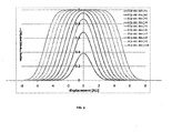
- optical shear sensor As for the optical aspect, two-dimensional calculations were performed to evaluate the response of an optical shear sensor according to one embodiment, for varying relative displacements between the photodetector and the optoelectronic source.
- the optoelectronic source (VCSEL) was modelled as a Gaussian beam with 5 micrometer beam waist and a (half) beam divergence of 7°.
- the active area of the photodetector was assumed to have a line shape with length d.
- the sensor response to a relative lateral displacement between the photodetector and the optoelectronic source was calculated for varying ratios between the detector size d and the laser beam diameter.
- the sensing element 100 shown in Figure 1 and Figure 2 comprises a single optoelectronic source 50 and a single photodetector 60.
- the sensing element 100 can comprise for example a single optoelectronic source 50 and more than one photodetector 60, e.g. arranged in an array. Such a configuration has a higher resolution and accuracy and allows for example determining the direction of a shear force.
- the sensing element 100 can comprise for example more than one optoelectronic source 50.
- a plurality of sensing elements 100 can be used for forming a sensor array or a tactile sensor.
- a two-dimensional array of sensing elements e.g. arranged in a matrix structure, can be used for performing area measurements.
- the sensing elements in such a two-dimensional array can be connected by stretchable interconnects, such that a stretchable shear sensor array can be formed.
- Arranging the plurality of sensing elements in an array allows measuring the shear direction.
- the first outer surface 81 is positioned along the photodetector 60 such that in other words the optoelectric source 50 and the photodetector 60 are arranged along the same outer surface, i.e.
- the second outer surface 82 comprises a reflector 80 for reflecting light emitted by the optoelectronic source 50 back to the photodetector 60 according to the displacement of the first outer surface 81 with respect to the second outer surface 82.
- the location and dimensions of the reflector 80 are adapted such that upon application of shear stress to the optical shear sensor, the light emitted by the optoelectric source 50 is no longer reflected by the reflector 80 to at least one photodetector 60.
- a shear stress to the left will cause that reflection of light emitted by the optoelectronic source 50 will cease to be reflected to photodetector 60, indicating that a shear stress is applied. If another photodetector 86 is positioned at the left of the optoelectronic source it becomes possible that light emitted by the optoelectronic source 50 is now detected at the second photodetector 86. In such case not only can be determined whether a shear stress is applied but in addition the direction of the shear stress can be determined.
- the reflector 80 is positioned and dimensioned such as to reflect light emitted by the optoelectronic source to both of the photodetectors 86, 60 when no shear stress is being applied, but upon application of a shear stress ceases to reflect light to one or even both of the photodetectors 60, 86 at least indicating that a shear stress has been applied and sometimes even indicating the direction of the shear stress, when for example only one photodetector still receives light emitted by the optoelectronic source 50 and reflected from the reflector 80.
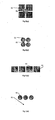
- Figures 5(a) - 5(d) show some additional embodiments according to the current invention in which the direction and/or the magnitude of the shear stress can be measured.
- the optoelectronic sources 50 and the photodetectors 60 are arranged in a stack. Such an arrangement is however not critical for the invention and the optoelectronic sources 50 and the photodetectors 60 can also both be positioned along the first outer surface 81.
- the sensing element 100 in these shown embodiments comprises a first group 91 of at least one optoelectronic source 50 and a second group 92 of at least one photodetector 60 arranged such that the direction and magnitude of the shear stress can be determined by determining which photodetector 60 of the second group 92 detects light emitted by which optoelectronic source 50.
- Figure 5a shows for example an embodiment wherein the first group 91 comprises an optoelectronic source 50 and the second group 92 an array of photodetectors, the first group 91 being positioned with respect to the second group 92 such that upon application of a shear stress the intensity measured by a first photodetector 60 of the array decreases while the intensity of a second photodetector 86 of the array increases, the change of intensity from the first photodetector 50 to the second photodetector 86 indicating the direction of the shear stress.
- the array of photodetectors may comprise four photodetectors arranged in a square-like configuration, the optoelectronic source 50 being positioned substantially in the center of the square-like configuration as such a configuration allows to determine the direction of the shear stress along all directions of the plane in which the photodetectors are provided.
- Figure 5b shows another example wherein the first group 91 comprises an array of different optoelectronic sources, such as for example optoelectronic sources emitting light of a different wavelength and/or emitting light having an intensity which is specifically modulated, and the second group 92 a photodetector 60, the first group 91 being positioned with respect to the second group 92 such that upon application of a shear stress the light measured by the photodetector 60 is indicative of the position of one of the optoelectronic sources of the array.
- the first group 91 comprises an array of different optoelectronic sources, such as for example optoelectronic sources emitting light of a different wavelength and/or emitting light having an intensity which is specifically modulated
- the second group 92 a photodetector 60
- the array of optoelectronic sources preferably comprises four optoelectronic sources arranged in a square-like configuration, the photodetector 60 being positioned substantially in the center of the square-like configuration as such a configuration allows to determine the direction of the shear stress along all directions of the plane in which the optoelectronic sources are provided.
- Figures 5c and 5d show that the first group 91 also comprises an array of optoelectronic sources.
- the arrays of the first 91 and the second 92 group are substantially linear, as shown in figure 5b and 5d .
- the linear arrays are positioned perpendicular with respect to each other and the optoelectronic sources are different, e.g. optoelectronic sources emitting light of a different wavelength and/or emitting light having an intensity which is specifically modulated to distinguish between the optoelectronic sources as in the earlier described embodiment.
- the two groups are positioned such that pairs of photodetectors and optoelectronic sources are formed.
- the optoelectronic source and the photodetector are optically aligned and part of the photodetector or part of the optoelectronic source is covered by a layer that is not transparent to the light emitted by the corresponding optoelectronic source , the part covered being different in each pair such that the intensities measured by the photodetector are indicative of the direction of the shear stress.
- the optoelectronic source and the photodetector are not optically aligned and the mutual position of the optoelectronic source and the photodetector in each pair are chosen such that upon application of a shear stress, the direction of the shear stress can be determined by determining which photodetectors detect light and the magnitude of the shear stress can be determined by measuring the intensities of the detected light.
- Fabrication of a shear sensor can comprise: providing an optoelectronic source 50 on a first substrate 11; embedding the optoelectronic source 50 in a first embedding layer 21; providing electrical contacts 41 to the optoelectronic source 50; providing a photodetector 60 on a second substrate 12; embedding the photodetector 60 in a second embedding layer 22; providing electrical contacts 42 to the photodetector 60; and bonding the first substrate 11 comprising the embedded optoelectronic source 50 to the second substrate comprising the embedded photodetector 60 such that the optoelectronic source 50 and the photodetector 60 are oriented face to face. Bonding can for example be done by means of a layer of silicone, acting as a sensing layer 30.
- a shear sensor e.g., a shear sensor comprising a plurality of sensing elements according to one embodiment, can be fabricated using a build-up process.
- Such a fabrication process may comprise: providing an optoelectronic source 50 on a first substrate 11; embedding the optoelectronic source 50 in a first embedding layer 21; providing electrical contacts 41 to the optoelectronic source 50; providing a sensing layer 30 on the first embedding layer 21 and the electrical contacts 41; providing electrical contacts 42 for the photodetector 60; mounting the photodetector 60 such that the optoelectronic source 50 and the photodetector 60 are oriented face to face; embedding the photodetector 60 in a second embedding layer 22; and providing the second substrate 12.
- beam shape of the light emitted by the optoelectronic source and the shape of the photodetector are adapted to each other and to the measurement.
- optical, preferably micro-optical, components such as micro lenses, filters, for examples filters for shaping the beam of the emitted light, for example to provide the beam with a linear profile in a certain direction or to make the characteristics of the emitted light dependent on the position of the optoelectronic source with respect to the photodetector such that, for example, the direction and/or magnitude of the shear stress can be measured.
- a shear sensor according to an embodiment of the present disclosure was fabricated.
- commercially available optoelectronic devices (1 x4 VCSEL array chip, 1x4 photodetector array chip) were thinned down to a thickness of 20 micrometer.
- the naked dies were mounted face down on a temporary glass carrier (i.e. with their front surface oriented to the temporary carrier) with a dedicated glycophtalate wax which proved good adhesion and optimized hardness to protect the brittle small GaAs dies during the lapping steps.
- Larger dummy GaAs dies were mounted in the same step next to the functional dies to allow a well controlled pressure distribution over the different dies.
- the dummies need to have the same thickness to guarantee a good die levelling after mounting.
- the wax was applied above its melting temperature and an extra load was provided on the dies to obtain a wax layer with a uniform thickness underneath the dies.
- the backside of the dies was then lapped on a glass plate with a slurry comprising about 9 micrometer thick Al 2 O 3 grains.
- the lapping was used to thin down the dies to a thickness of 50 micrometer. After that, an additional about 30 micrometer was removed by means of a polishing step on a soft tissue with an Al 2 O 3 grain size of about 0.3 micrometer. After the polishing step the dies were removed from the temporary glass carrier.
- the dies were embedded in an ultra thin flexible package.
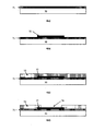
- This embedding or packaging step was performed on a temporary rigid carrier, as illustrated in Figure 4 .
- This step was performed separately for a VCSEL and for a photodetector.
- a thin polyimide layer 71 with a thickness in the range between 8 micrometer and 10 micrometer was provided by spin coating ( Figure 4(a) ).
- an adhesion promotor only at the edges of the glass carrier, the polyimide only adheres to the glass at the edges, enabling simple release of the package from the carrier after fabrication.
- other release techniques known to a person skilled in the art can be used, such as for example techniques using thermal release tape.
- metal islands 72 On top of the polyimide layer 71, 10 micrometer thick metal islands 72 (Cu) were formed by a consecutive sputter, plate and wet etch process ( Figure 4(b) ). Other techniques known to a person skilled in the art may be used for forming the metal islands. For example, lamination may be used instead of plating. In the final package, these islands 72 act as a heat buffer for the embedded VCSEL or photodetector.
- the optoelectronic devices 75 such as VCSEL chips and the photodetector chips, used in the experiments only had top electrical contacts. When using optoelectronic sources and/or photodetectors having top and bottom contacts, the metal layer 72 may also be used for forming electrical contacts to the optoelectronic source and/or photodetector.
- a 20 micrometer thick layer of optical transparent embedding material 73 (Truemode Backplane Polymer TM ) was spin coated, as illustrated in Figure 4(c) .
- a cavity 74 was formed by ablation with a KrF excimer laser (wavelength 248 nm), using the metal islands 72 as a laser stop ( Figure 4(d) ). This results in a cavity 74 with a flat bottom.
- Other methods known to a person skilled in the art may be used for forming the cavity 74, such as for example lithography methods.
- a low viscosity underfill material for flip-chip applications (U 8449-9 from Namics Corporation) was used as an adhesive (not illustrated) to mount the optoelectronic device 75 inside the cavity 74.
- the die angle with respect to the substrate after hardening of the adhesive can be limited.
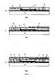
- a second layer 76 (about 5 ⁇ m thick) of optical transparent material was spin-coated, which makes the die completely embedded. The resulting structure is schematically shown in Figure 4(e) .
- micro-via's were created towards the contact pads of the embedded die 75, by means of a KrF Excimer laser.
- a sputter and etch process was then used for providing copper tracks 77 from within the vias towards larger pitch contacts on the package ( Figure 4(f) ).
- a final layer 78 of optical transparent material (thickness 5 ⁇ m) was provided for filling the vias; this layer also acts as a final planarization layer.
- a second polyimide layer 79 was spin-coated and cured. The resulting structure (thin optoelectronic package) is shown in Figure 4(g) .
- the top polyimide layer 79 and the bottom polyimide layer 71 act in this case as mechanical supporting layers. According to the principle of the neutral fiber, most of the stress during bending is taken up by the outer layers of the stack, being the strong polyimide layers. This technology protects the inner optical layers. Commercially available optical materials are often not very strong and flexible, but with a total thickness of only about 40 ⁇ m and a build-up with supporting polyimide layers, all materials can be bended to some extent. In embodiments of the present disclosure polyimides can also be used for forming the embedding layers 73, 76 and 78.
- a first optoelectronic package (as shown in Figure 4(g) ) comprising an embedded VCSEL chip (optoelectronic device 75 in Figure 4(g) ) and a second optoelectronic package comprising an embedded photodetector chip (optoelectronic device 75 in Figure 4(g) ) were covered with a thin layer of PDMS (Sylgard 184) as sensing layer.
- the separate modules were cut-out using a CO 2 laser.
- they were bonded face to face with the sensing layers facing each other onto each other to obtain a shear sensor according to one embodiment, as shown in Figure 1 .
- the optoelectronic source and a photodetector within a sensing element are optically aligned to each other. Aligning both elements can be done passively or actively. Passive alignment generally refers to a procedure using optical or mechanical alignment marks onto the two substrates which need to be aligned. During active alignment, the optoelectronic source is connected to a power source, and the alignment is achieved by maximizing the electrical current generated by the photodiode.
Landscapes
- Physics & Mathematics (AREA)
- General Physics & Mathematics (AREA)
- Force Measurement Appropriate To Specific Purposes (AREA)
Claims (20)
- Optischer Schersensor, umfassend eine erste (81) und eine zweite (82) Außenfläche auf gegenüberliegenden Seiten des optischen Schersensors und mindestens ein Sensorelement (100), wobei das mindestens eine Sensorelement (100) eine optoelektronische Quelle (50), um Licht einer vorbestimmten Wellenlänge zu emittieren, wobei die optoelektronische Quelle (50) eine Quellenvorderfläche (51) aufweist, welche die Außenfläche der optoelektronischen Quelle (50) ist, an der Licht der vorbestimmten Wellenlänge die optoelektronische Quelle (50) verlässt, und mindestens einen Photodetektor (60) zum Erkennen von Licht der vorbestimmten Wellenlänge umfasst, wobei der mindestens eine Photodetektor (60) eine Detektorvorderfläche (61) aufweist, welche die Außenfläche des Photodetektors (60) ist, an der Licht der optoelektronischen Quelle (50) bereitgestellt wird, um empfangen zu werden, wobei die optoelektronische Quelle (50) entlang der ersten Oberfläche (81) positioniert ist und Licht in Richtung auf die zweite Oberfläche (82) emittiert, dadurch gekennzeichnet, dass eine biegsame Sensorschicht (30) sowohl die Vorderfläche der optoelektronischen Quelle (50) als auch die Vorderfläche des Photodetektors (60) bedeckt, wobei die Sensorschicht (30) für die vorbestimmte Wellenlänge transparent ist, und dass die optoelektronische Quelle (50), der Photodetektor (60), die zweite Außenfläche (82) und die Sensorschicht (30) derart angeordnet sind, dass sich beim Anwenden einer Scherspannung auf den optischen Schersensor die Sensorschicht (30) elastisch verformt und die ersten (81) und zweiten (82) Außenflächen in Richtungen verschoben werden, die zueinander und zu der Quellenvorderfläche parallel sind, so dass sich die Intensität des Lichts, das von der optoelektronischen Quelle (50) emittiert wird und von dem Photodetektor (60) erkannt wird, ändert, wobei die Änderung der Intensität des Lichts, das von der optoelektronischen Quelle (50) emittiert und von dem Photodetektor (60) erkannt wird, die angewendete Scherspannung angibt.
- Optischer Schersensor nach Anspruch 1, dadurch gekennzeichnet, dass die optoelektronische Quelle (50) und der mindestens eine Photodetektor (60) in einem Stapel angeordnet sind, wobei der Photodetektor (60) entlang der zweiten Oberfläche (82) positioniert ist, so dass die Quellenvorderfläche und die Detektorvorderfläche im Wesentlichen parallel und einander zugewandt sind, wobei sich die Sensorschicht (30) zwischen der optoelektronischen Quelle (50) und dem mindestens einen Photodetektor (60) befindet, und dass die optoelektronische Quelle (50), der Photodetektor (60) und die Sensorschicht (30) derart angeordnet sind, dass sich bei Anwendung einer Scherspannung auf den optischen Schersensor die Sensorschicht (30) derart verformt, dass die optoelektronische Quelle (50) und der Photodetektor (60) im Verhältnis zueinander in Richtungen verschoben werden, die zueinander und zu der Quellenvorderfläche parallel sind.
- Optischer Schersensor nach Anspruch 1, dadurch gekennzeichnet, dass der Photodetektor entlang der ersten Außenfläche (81) positioniert ist, wobei die zweite Außenfläche (82) einen Reflektor (80) umfasst, um Licht zu reflektieren, das von der optoelektronischen Quelle (50) gemäß der Verschiebung der ersten Außenfläche (81) im Verhältnis zu der zweiten Außenfläche (82) zurück auf den Photodetektor (60) emittiert wird.
- Optischer Schersensor nach einem der Ansprüche 1 bis 3, dadurch gekennzeichnet, dass die optoelektronische Quelle (50) ohne Vorliegen von Scherspannung optisch auf einen Photodetektor (60) ausgerichtet ist.
- Optischer Schersensor nach einem der Ansprüche 1 bis 3, dadurch gekennzeichnet, dass bei Vorliegen der Scherspannung am Sensor in einer Ebene parallel zu der Quellenvorderfläche die optoelektronische Quelle (50) optisch auf einen Photodetektor (60) ausgerichtet ist.
- Optischer Schersensor nach einem der Ansprüche 1 bis 5, dadurch gekennzeichnet, dass das mindestens eine Sensorelement (100) ferner elektrische Kontakte (41, 42) mit der optoelektronischen Quelle (50) und dem Photodetektor (60) umfasst.
- Optischer Schersensor nach einem der Ansprüche 1 bis 6 mindestens kombiniert mit Anspruch 2, dadurch gekennzeichnet, dass die optoelektronische Quelle (50) in einer ersten Einbettungsschicht (11) eingebettet ist, wobei der mindestens eine Photodetektor (60) in einer zweiten Einbettungsschicht (12) eingebettet ist, und wobei die Sensorschicht (30) zwischen der ersten Einbettungsschicht (11) und der zweiten Einbettungsschicht (12) eingeschoben ist.
- Optischer Schersensor nach Anspruch 7, dadurch gekennzeichnet, dass die erste Einbettungsschicht (11) und die zweite Einbettungsschicht (12) ein biegsames Material umfassen.
- Optischer Schersensor nach Anspruch 7 oder 8, dadurch gekennzeichnet, dass die erste Einbettungsschicht (11) und die zweite Einbettungsschicht (12) ein dehnbares Material umfassen.
- Optischer Schersensor nach einem der Ansprüche 1 bis 9, dadurch gekennzeichnet, dass die Sensorschicht (30) biegsam ist.
- Optischer Schersensor nach einem der Ansprüche 1 bis 10, dadurch gekennzeichnet, dass die Sensorschicht (30) dehnbar ist.
- Optischer Schersensor nach einem der Ansprüche 1 bis 11, mindestens kombiniert mit Anspruch 10 und 8, dadurch gekennzeichnet, dass der Sensor biegsam ist.
- Optischer Schersensor nach einem der Ansprüche 1 bis 12, mindestens kombiniert mit Anspruch 11 und 9, dadurch gekennzeichnet, dass der Sensor dehnbar ist.
- Optischer Schersensor nach einem der Ansprüche 1 bis 13, dadurch gekennzeichnet, dass die Sensorschicht (30) ein Polymer, ein Polyurethan oder ein Silikon umfasst.
- Optischer Schersensor nach einem der Ansprüche 1 bis 14, dadurch gekennzeichnet, dass die Sensorschicht (30) eine geringe Hysterese und einen Schermodul im Bereich zwischen ungefähr 100 kPa und 300 MPa aufweist.
- Optischer Schersensor nach einem der Ansprüche 1 bis 15, dadurch gekennzeichnet, dass der Schersensor eine Vielzahl von Sensorelementen (100) umfasst, die in einer zweidimensionalen Aufstellung angeordnet ist.
- Optischer Schersensor nach einem der Ansprüche 1 bis 16, dadurch gekennzeichnet, dass das Sensorelement (100) eine erste Gruppe (91) aus mindestens einer optoelektronischen Quelle (50) und eine zweite Gruppe (92) aus mindestens einem Photodetektor (60) umfasst, die derart angeordnet sind, dass die Richtung und/oder die Größe der Scherspannung bestimmt werden kann bzw. können, indem bestimmt wird, welcher Photodetektor (60) der zweiten Gruppe (92) das Licht erkennt, das von der optoelektronischen Quelle (50) der ersten Gruppe (91) emittiert wird.
- Verfahren zum Herstellen eines optischen Schersensors nach einem der Ansprüche 1 bis 16, kombiniert mit mindestens Anspruch 2, 5 und 6, dadurch gekennzeichnet, dass das Verfahren folgende Schritte umfasst: Bereitstellen der optoelektronischen Quelle (50) auf einem ersten Substrat (11); Einbetten der optoelektronischen Quelle (50) in die erste Einbettungsschicht (21); Bereitstellen der elektrischen Kontakte (41) mit der optoelektronischen Quelle (50); Bereitstellen des Photodetektors (60) auf einem zweiten Substrat (12); Einbetten des Photodetektors (60) in die zweite Einbettungsschicht (22); Bereitstellen der elektrischen Kontakte (42) mit dem Photodetektor (60); und Verbinden des ersten Substrats (11), das die eingebettete optoelektronische Quelle (50) umfasst, mit dem zweiten Substrat, das den eingebetteten Photodetektor (60) umfasst, über die Sensorschicht, so dass die Vorderfläche der optoelektronischen Quelle (50) und des Photodetektors (60) im Wesentlichen parallel und einander zugewandt sind.
- Verfahren zum Herstellen eines optischen Schersensors nach Anspruch 18, dadurch gekennzeichnet, dass die Schritte des Bereitstellens der optoelektronischen Quelle (50) auf einem ersten Substrat (11); des Einbettens der optoelektronischen Quelle (50) in die erste Einbettungsschicht (21); des Bereitstellens der elektrischen Kontakte (41) mit der optoelektronischen Quelle (50); und die Schritte des Bereitstellens des Photodetektors (60) auf einem zweiten Substrat (12); des Einbettens des Photodetektors (60) in die zweite Einbettungsschicht (22); des Bereitstellens der elektrischen Kontakte (42) mit dem Photodetektor (60); getrennt erfolgen, woraufhin das erste Substrat (11), das die eingebettete optoelektronische Quelle (50) umfasst, mit dem zweiten Substrat, das den eingebetteten Photodetektor (60) umfasst, über die Sensorschicht verbunden wird, so dass die optoelektronische Quelle (50) und der Photodetektor (60) im Wesentlichen parallel und einander zugewandt sind.
- Verfahren zum Herstellen eines optischen Schersensors nach Anspruch 18, dadurch gekennzeichnet, dass das Verfahren ein Aufbauprozess ist, der die folgenden aufeinanderfolgenden Schritte umfasst: Bereitstellen der optoelektronischen Quelle (50) auf einem ersten Substrat (11); Einbetten der optoelektronischen Quelle (50) in die erste Einbettungsschicht (21); Bereitstellen der ersten elektrischen Kontakte (41) mit der optoelektronischen Quelle (50); Bereitstellen der Sensorschicht (30) auf der ersten Einbettungsschicht (21) und der ersten elektrischen Kontakte (41); Bereitstellen der zweiten elektrischen Kontakte (42) für den Photodetektor (60) mit der Sensorschicht (30); Bereitstellen des Photodetektors (60) an den zweiten elektrischen Kontakten (42), so dass die Vorderfläche des Photodetektors (60) und die Vorderfläche der optoelektronischen Quelle (50) im Wesentlichen parallel und einander zugewandt sind; Einbetten des Photodetektors (60) in die zweite Einbettungsschicht (22).
Applications Claiming Priority (2)
| Application Number | Priority Date | Filing Date | Title |
|---|---|---|---|
| US32308110P | 2010-04-12 | 2010-04-12 | |
| PCT/EP2011/055517 WO2011128266A1 (en) | 2010-04-12 | 2011-04-08 | Optical shear sensor and method of producing such an optical shear sensor |
Publications (2)
| Publication Number | Publication Date |
|---|---|
| EP2558832A1 EP2558832A1 (de) | 2013-02-20 |
| EP2558832B1 true EP2558832B1 (de) | 2015-01-07 |
Family
ID=44501637
Family Applications (1)
| Application Number | Title | Priority Date | Filing Date |
|---|---|---|---|
| EP11717208.0A Not-in-force EP2558832B1 (de) | 2010-04-12 | 2011-04-08 | Optischer schersensor und verfahren zur herstellung eines derartigen optischen schersensors |
Country Status (3)
| Country | Link |
|---|---|
| US (1) | US8780335B2 (de) |
| EP (1) | EP2558832B1 (de) |
| WO (1) | WO2011128266A1 (de) |
Families Citing this family (12)
| Publication number | Priority date | Publication date | Assignee | Title |
|---|---|---|---|---|
| TWI482953B (zh) * | 2012-12-28 | 2015-05-01 | Univ Nat Chiao Tung | 壓力與剪力量測裝置及方法 |
| US9518882B2 (en) * | 2013-07-03 | 2016-12-13 | The Cleveland Electric Laboratories Company | Optical multi-axis force sensor |
| WO2015069260A1 (en) * | 2013-11-07 | 2015-05-14 | Schlumberger Canada Limited | Characterization of fluids with drag reducing additives in a couette device |
| US10114510B2 (en) | 2013-12-23 | 2018-10-30 | Samsung Display Co., Ltd. | Apparatus and method for detecting surface shear force on a display device |
| JP6462009B2 (ja) * | 2015-02-05 | 2019-01-30 | 三井化学株式会社 | 光弾性ポリウレタン樹脂、検知部材、ロボット、および、光弾性ポリウレタン樹脂の製造方法 |
| US10206288B2 (en) | 2015-08-13 | 2019-02-12 | Palo Alto Research Center Incorporated | Bare die integration with printed components on flexible substrate |
| US10165677B2 (en) * | 2015-12-10 | 2018-12-25 | Palo Alto Research Center Incorporated | Bare die integration with printed components on flexible substrate without laser cut |
| US10041856B2 (en) | 2016-03-01 | 2018-08-07 | Cleveland Electric Laboratories Company | Method and apparatus for measuring physical displacement |
| US10847384B2 (en) | 2017-05-31 | 2020-11-24 | Palo Alto Research Center Incorporated | Method and fixture for chip attachment to physical objects |
| WO2019060870A1 (en) * | 2017-09-25 | 2019-03-28 | Kent State University | APPARATUS FOR MEASURING THE PROFILE OF A NORMAL STRESS AND SHEARING OF A SURFACE |
| US12092544B2 (en) * | 2018-09-10 | 2024-09-17 | The University Of British Columbia | Optical force sensors |
| JP7036236B2 (ja) | 2019-02-15 | 2022-03-15 | 株式会社村田製作所 | 触覚及び近接センサ |
Family Cites Families (5)
| Publication number | Priority date | Publication date | Assignee | Title |
|---|---|---|---|---|
| ATE145725T1 (de) * | 1991-04-26 | 1996-12-15 | Scherrer Inst Paul | Verfahren und vorrichtung zur bestimmung einer messgrösse mittels eines integriert-optischen sensormoduls |
| US6717172B2 (en) * | 2000-12-19 | 2004-04-06 | California Institute Of Technology | Diffractive optical fluid shear stress sensor |
| US7466879B2 (en) | 2003-05-22 | 2008-12-16 | Nanyang Technological University | Fiber optic force sensor for measuring shear force |
| US7295724B2 (en) | 2004-03-01 | 2007-11-13 | University Of Washington | Polymer based distributive waveguide sensor for pressure and shear measurement |
| JP5449336B2 (ja) * | 2008-06-19 | 2014-03-19 | マサチューセッツ インスティテュート オブ テクノロジー | 弾性撮像を使用する接触センサ |
-
2011
- 2011-04-08 WO PCT/EP2011/055517 patent/WO2011128266A1/en not_active Ceased
- 2011-04-08 EP EP11717208.0A patent/EP2558832B1/de not_active Not-in-force
-
2012
- 2012-10-02 US US13/633,570 patent/US8780335B2/en not_active Expired - Fee Related
Also Published As
| Publication number | Publication date |
|---|---|
| EP2558832A1 (de) | 2013-02-20 |
| US8780335B2 (en) | 2014-07-15 |
| US20130036829A1 (en) | 2013-02-14 |
| WO2011128266A1 (en) | 2011-10-20 |
Similar Documents
| Publication | Publication Date | Title |
|---|---|---|
| US8780335B2 (en) | Optical shear sensor and method of producing such an optical shear sensor | |
| US8567257B2 (en) | Optical tactile sensors | |
| EP2195628B1 (de) | Optischer sensor zur messung einer kraftverteilung | |
| US7295724B2 (en) | Polymer based distributive waveguide sensor for pressure and shear measurement | |
| US8646335B2 (en) | Contact stress sensor | |
| Missinne et al. | Two axis optoelectronic tactile shear stress sensor | |
| Missinne et al. | Flexible shear sensor based on embedded optoelectronic components | |
| Bosman et al. | Ultrathin optoelectronic device packaging in flexible carriers | |
| TW561288B (en) | Passively aligned fiber optical engine for parallel optics interconnect devices | |
| CN113686548A (zh) | 附着至光子芯片的激光器的晶圆级测试 | |
| WO2014014414A1 (en) | Sensor module and method of manufacturing the same | |
| US20150108334A1 (en) | Optical Sensor Module | |
| Takeshita et al. | Development and evaluation of a two-axial shearing force sensor consisting of an optical sensor chip and elastic gum frame | |
| Missinne et al. | Embedded flexible optical shear sensor | |
| US10365431B2 (en) | Optical interconnect structure | |
| CN112710247A (zh) | 一种表面粘贴式光纤光栅应变传感器封装方法 | |
| KR20160066521A (ko) | 광 결정 센서 구조 및 그 제조 방법 | |
| Bosman et al. | Unobtrusive packaging of optoelectronic devices for optical tactile and shear sensors | |
| US20160025483A1 (en) | Pre-formed optical meander structures for use in an optical strain gauge system for measuing strain, and a method | |
| Missinne et al. | Ultra thin optical tactile shear sensor | |
| Van Hoe et al. | Novel coupling and packaging approaches for optical interconnects | |
| Missinne et al. | Ultra-thin multi-axial shear stress sensor based on a segmented photodiode | |
| Wang et al. | Development of a directional sensitive pressure and shear sensor | |
| Bosman et al. | Fully embedded optical and electrical interconnections in flexible foils | |
| WO2025221950A1 (en) | High resolution photonic tactile sensor |
Legal Events
| Date | Code | Title | Description |
|---|---|---|---|
| PUAI | Public reference made under article 153(3) epc to a published international application that has entered the european phase |
Free format text: ORIGINAL CODE: 0009012 |
|
| 17P | Request for examination filed |
Effective date: 20120914 |
|
| AK | Designated contracting states |
Kind code of ref document: A1 Designated state(s): AL AT BE BG CH CY CZ DE DK EE ES FI FR GB GR HR HU IE IS IT LI LT LU LV MC MK MT NL NO PL PT RO RS SE SI SK SM TR |
|
| DAX | Request for extension of the european patent (deleted) | ||
| GRAP | Despatch of communication of intention to grant a patent |
Free format text: ORIGINAL CODE: EPIDOSNIGR1 |
|
| INTG | Intention to grant announced |
Effective date: 20131219 |
|
| GRAP | Despatch of communication of intention to grant a patent |
Free format text: ORIGINAL CODE: EPIDOSNIGR1 |
|
| INTG | Intention to grant announced |
Effective date: 20140616 |
|
| GRAS | Grant fee paid |
Free format text: ORIGINAL CODE: EPIDOSNIGR3 |
|
| GRAA | (expected) grant |
Free format text: ORIGINAL CODE: 0009210 |
|
| RAP1 | Party data changed (applicant data changed or rights of an application transferred) |
Owner name: UNIVERSITEIT GENT Owner name: IMEC VZW |
|
| AK | Designated contracting states |
Kind code of ref document: B1 Designated state(s): AL AT BE BG CH CY CZ DE DK EE ES FI FR GB GR HR HU IE IS IT LI LT LU LV MC MK MT NL NO PL PT RO RS SE SI SK SM TR |
|
| REG | Reference to a national code |
Ref country code: GB Ref legal event code: FG4D |
|
| REG | Reference to a national code |
Ref country code: CH Ref legal event code: EP |
|
| REG | Reference to a national code |
Ref country code: IE Ref legal event code: FG4D |
|
| REG | Reference to a national code |
Ref country code: AT Ref legal event code: REF Ref document number: 706042 Country of ref document: AT Kind code of ref document: T Effective date: 20150215 |
|
| REG | Reference to a national code |
Ref country code: DE Ref legal event code: R096 Ref document number: 602011012886 Country of ref document: DE Effective date: 20150305 |
|
| REG | Reference to a national code |
Ref country code: NL Ref legal event code: VDEP Effective date: 20150107 |
|
| REG | Reference to a national code |
Ref country code: AT Ref legal event code: MK05 Ref document number: 706042 Country of ref document: AT Kind code of ref document: T Effective date: 20150107 |
|
| REG | Reference to a national code |
Ref country code: LT Ref legal event code: MG4D |
|
| PG25 | Lapsed in a contracting state [announced via postgrant information from national office to epo] |
Ref country code: SE Free format text: LAPSE BECAUSE OF FAILURE TO SUBMIT A TRANSLATION OF THE DESCRIPTION OR TO PAY THE FEE WITHIN THE PRESCRIBED TIME-LIMIT Effective date: 20150107 Ref country code: LT Free format text: LAPSE BECAUSE OF FAILURE TO SUBMIT A TRANSLATION OF THE DESCRIPTION OR TO PAY THE FEE WITHIN THE PRESCRIBED TIME-LIMIT Effective date: 20150107 Ref country code: FI Free format text: LAPSE BECAUSE OF FAILURE TO SUBMIT A TRANSLATION OF THE DESCRIPTION OR TO PAY THE FEE WITHIN THE PRESCRIBED TIME-LIMIT Effective date: 20150107 Ref country code: HR Free format text: LAPSE BECAUSE OF FAILURE TO SUBMIT A TRANSLATION OF THE DESCRIPTION OR TO PAY THE FEE WITHIN THE PRESCRIBED TIME-LIMIT Effective date: 20150107 Ref country code: BG Free format text: LAPSE BECAUSE OF FAILURE TO SUBMIT A TRANSLATION OF THE DESCRIPTION OR TO PAY THE FEE WITHIN THE PRESCRIBED TIME-LIMIT Effective date: 20150407 Ref country code: NO Free format text: LAPSE BECAUSE OF FAILURE TO SUBMIT A TRANSLATION OF THE DESCRIPTION OR TO PAY THE FEE WITHIN THE PRESCRIBED TIME-LIMIT Effective date: 20150407 Ref country code: ES Free format text: LAPSE BECAUSE OF FAILURE TO SUBMIT A TRANSLATION OF THE DESCRIPTION OR TO PAY THE FEE WITHIN THE PRESCRIBED TIME-LIMIT Effective date: 20150107 |
|
| PG25 | Lapsed in a contracting state [announced via postgrant information from national office to epo] |
Ref country code: IS Free format text: LAPSE BECAUSE OF FAILURE TO SUBMIT A TRANSLATION OF THE DESCRIPTION OR TO PAY THE FEE WITHIN THE PRESCRIBED TIME-LIMIT Effective date: 20150507 Ref country code: AT Free format text: LAPSE BECAUSE OF FAILURE TO SUBMIT A TRANSLATION OF THE DESCRIPTION OR TO PAY THE FEE WITHIN THE PRESCRIBED TIME-LIMIT Effective date: 20150107 Ref country code: GR Free format text: LAPSE BECAUSE OF FAILURE TO SUBMIT A TRANSLATION OF THE DESCRIPTION OR TO PAY THE FEE WITHIN THE PRESCRIBED TIME-LIMIT Effective date: 20150408 Ref country code: NL Free format text: LAPSE BECAUSE OF FAILURE TO SUBMIT A TRANSLATION OF THE DESCRIPTION OR TO PAY THE FEE WITHIN THE PRESCRIBED TIME-LIMIT Effective date: 20150107 Ref country code: PL Free format text: LAPSE BECAUSE OF FAILURE TO SUBMIT A TRANSLATION OF THE DESCRIPTION OR TO PAY THE FEE WITHIN THE PRESCRIBED TIME-LIMIT Effective date: 20150107 Ref country code: LV Free format text: LAPSE BECAUSE OF FAILURE TO SUBMIT A TRANSLATION OF THE DESCRIPTION OR TO PAY THE FEE WITHIN THE PRESCRIBED TIME-LIMIT Effective date: 20150107 Ref country code: RS Free format text: LAPSE BECAUSE OF FAILURE TO SUBMIT A TRANSLATION OF THE DESCRIPTION OR TO PAY THE FEE WITHIN THE PRESCRIBED TIME-LIMIT Effective date: 20150107 |
|
| REG | Reference to a national code |
Ref country code: DE Ref legal event code: R097 Ref document number: 602011012886 Country of ref document: DE |
|
| PG25 | Lapsed in a contracting state [announced via postgrant information from national office to epo] |
Ref country code: RO Free format text: LAPSE BECAUSE OF FAILURE TO SUBMIT A TRANSLATION OF THE DESCRIPTION OR TO PAY THE FEE WITHIN THE PRESCRIBED TIME-LIMIT Effective date: 20150107 Ref country code: DK Free format text: LAPSE BECAUSE OF FAILURE TO SUBMIT A TRANSLATION OF THE DESCRIPTION OR TO PAY THE FEE WITHIN THE PRESCRIBED TIME-LIMIT Effective date: 20150107 Ref country code: SK Free format text: LAPSE BECAUSE OF FAILURE TO SUBMIT A TRANSLATION OF THE DESCRIPTION OR TO PAY THE FEE WITHIN THE PRESCRIBED TIME-LIMIT Effective date: 20150107 Ref country code: CZ Free format text: LAPSE BECAUSE OF FAILURE TO SUBMIT A TRANSLATION OF THE DESCRIPTION OR TO PAY THE FEE WITHIN THE PRESCRIBED TIME-LIMIT Effective date: 20150107 Ref country code: EE Free format text: LAPSE BECAUSE OF FAILURE TO SUBMIT A TRANSLATION OF THE DESCRIPTION OR TO PAY THE FEE WITHIN THE PRESCRIBED TIME-LIMIT Effective date: 20150107 |
|
| PLBE | No opposition filed within time limit |
Free format text: ORIGINAL CODE: 0009261 |
|
| STAA | Information on the status of an ep patent application or granted ep patent |
Free format text: STATUS: NO OPPOSITION FILED WITHIN TIME LIMIT |
|
| PG25 | Lapsed in a contracting state [announced via postgrant information from national office to epo] |
Ref country code: LU Free format text: LAPSE BECAUSE OF FAILURE TO SUBMIT A TRANSLATION OF THE DESCRIPTION OR TO PAY THE FEE WITHIN THE PRESCRIBED TIME-LIMIT Effective date: 20150408 Ref country code: MC Free format text: LAPSE BECAUSE OF FAILURE TO SUBMIT A TRANSLATION OF THE DESCRIPTION OR TO PAY THE FEE WITHIN THE PRESCRIBED TIME-LIMIT Effective date: 20150107 |
|
| REG | Reference to a national code |
Ref country code: CH Ref legal event code: PL |
|
| 26N | No opposition filed |
Effective date: 20151008 |
|
| PG25 | Lapsed in a contracting state [announced via postgrant information from national office to epo] |
Ref country code: IT Free format text: LAPSE BECAUSE OF FAILURE TO SUBMIT A TRANSLATION OF THE DESCRIPTION OR TO PAY THE FEE WITHIN THE PRESCRIBED TIME-LIMIT Effective date: 20150107 |
|
| REG | Reference to a national code |
Ref country code: IE Ref legal event code: MM4A |
|
| PG25 | Lapsed in a contracting state [announced via postgrant information from national office to epo] |
Ref country code: CH Free format text: LAPSE BECAUSE OF NON-PAYMENT OF DUE FEES Effective date: 20150430 Ref country code: LI Free format text: LAPSE BECAUSE OF NON-PAYMENT OF DUE FEES Effective date: 20150430 |
|
| PG25 | Lapsed in a contracting state [announced via postgrant information from national office to epo] |
Ref country code: SI Free format text: LAPSE BECAUSE OF FAILURE TO SUBMIT A TRANSLATION OF THE DESCRIPTION OR TO PAY THE FEE WITHIN THE PRESCRIBED TIME-LIMIT Effective date: 20150107 |
|
| REG | Reference to a national code |
Ref country code: FR Ref legal event code: PLFP Year of fee payment: 6 |
|
| PG25 | Lapsed in a contracting state [announced via postgrant information from national office to epo] |
Ref country code: IE Free format text: LAPSE BECAUSE OF NON-PAYMENT OF DUE FEES Effective date: 20150408 |
|
| PG25 | Lapsed in a contracting state [announced via postgrant information from national office to epo] |
Ref country code: BE Free format text: LAPSE BECAUSE OF FAILURE TO SUBMIT A TRANSLATION OF THE DESCRIPTION OR TO PAY THE FEE WITHIN THE PRESCRIBED TIME-LIMIT Effective date: 20150107 |
|
| PG25 | Lapsed in a contracting state [announced via postgrant information from national office to epo] |
Ref country code: MT Free format text: LAPSE BECAUSE OF FAILURE TO SUBMIT A TRANSLATION OF THE DESCRIPTION OR TO PAY THE FEE WITHIN THE PRESCRIBED TIME-LIMIT Effective date: 20150107 |
|
| REG | Reference to a national code |
Ref country code: FR Ref legal event code: PLFP Year of fee payment: 7 |
|
| PG25 | Lapsed in a contracting state [announced via postgrant information from national office to epo] |
Ref country code: HU Free format text: LAPSE BECAUSE OF FAILURE TO SUBMIT A TRANSLATION OF THE DESCRIPTION OR TO PAY THE FEE WITHIN THE PRESCRIBED TIME-LIMIT; INVALID AB INITIO Effective date: 20110408 Ref country code: SM Free format text: LAPSE BECAUSE OF FAILURE TO SUBMIT A TRANSLATION OF THE DESCRIPTION OR TO PAY THE FEE WITHIN THE PRESCRIBED TIME-LIMIT Effective date: 20150107 |
|
| PG25 | Lapsed in a contracting state [announced via postgrant information from national office to epo] |
Ref country code: CY Free format text: LAPSE BECAUSE OF FAILURE TO SUBMIT A TRANSLATION OF THE DESCRIPTION OR TO PAY THE FEE WITHIN THE PRESCRIBED TIME-LIMIT Effective date: 20150107 |
|
| PG25 | Lapsed in a contracting state [announced via postgrant information from national office to epo] |
Ref country code: PT Free format text: LAPSE BECAUSE OF FAILURE TO SUBMIT A TRANSLATION OF THE DESCRIPTION OR TO PAY THE FEE WITHIN THE PRESCRIBED TIME-LIMIT Effective date: 20150507 |
|
| PG25 | Lapsed in a contracting state [announced via postgrant information from national office to epo] |
Ref country code: TR Free format text: LAPSE BECAUSE OF FAILURE TO SUBMIT A TRANSLATION OF THE DESCRIPTION OR TO PAY THE FEE WITHIN THE PRESCRIBED TIME-LIMIT Effective date: 20150107 |
|
| REG | Reference to a national code |
Ref country code: FR Ref legal event code: PLFP Year of fee payment: 8 |
|
| PG25 | Lapsed in a contracting state [announced via postgrant information from national office to epo] |
Ref country code: MK Free format text: LAPSE BECAUSE OF FAILURE TO SUBMIT A TRANSLATION OF THE DESCRIPTION OR TO PAY THE FEE WITHIN THE PRESCRIBED TIME-LIMIT Effective date: 20150107 |
|
| PG25 | Lapsed in a contracting state [announced via postgrant information from national office to epo] |
Ref country code: AL Free format text: LAPSE BECAUSE OF FAILURE TO SUBMIT A TRANSLATION OF THE DESCRIPTION OR TO PAY THE FEE WITHIN THE PRESCRIBED TIME-LIMIT Effective date: 20150107 |
|
| PGFP | Annual fee paid to national office [announced via postgrant information from national office to epo] |
Ref country code: GB Payment date: 20200323 Year of fee payment: 10 |
|
| PGFP | Annual fee paid to national office [announced via postgrant information from national office to epo] |
Ref country code: FR Payment date: 20200319 Year of fee payment: 10 |
|
| PGFP | Annual fee paid to national office [announced via postgrant information from national office to epo] |
Ref country code: DE Payment date: 20200319 Year of fee payment: 10 |
|
| REG | Reference to a national code |
Ref country code: DE Ref legal event code: R119 Ref document number: 602011012886 Country of ref document: DE |
|
| GBPC | Gb: european patent ceased through non-payment of renewal fee |
Effective date: 20210408 |
|
| PG25 | Lapsed in a contracting state [announced via postgrant information from national office to epo] |
Ref country code: GB Free format text: LAPSE BECAUSE OF NON-PAYMENT OF DUE FEES Effective date: 20210408 Ref country code: FR Free format text: LAPSE BECAUSE OF NON-PAYMENT OF DUE FEES Effective date: 20210430 Ref country code: DE Free format text: LAPSE BECAUSE OF NON-PAYMENT OF DUE FEES Effective date: 20211103 |