EP2559143B1 - Modularer multilevel umrichter mit sperrfilter für zweite und dritte harmonische - Google Patents
Modularer multilevel umrichter mit sperrfilter für zweite und dritte harmonische Download PDFInfo
- Publication number
- EP2559143B1 EP2559143B1 EP10713679.8A EP10713679A EP2559143B1 EP 2559143 B1 EP2559143 B1 EP 2559143B1 EP 10713679 A EP10713679 A EP 10713679A EP 2559143 B1 EP2559143 B1 EP 2559143B1
- Authority
- EP
- European Patent Office
- Prior art keywords
- energy storage
- elements
- storage element
- filter
- storage elements
- Prior art date
- Legal status (The legal status is an assumption and is not a legal conclusion. Google has not performed a legal analysis and makes no representation as to the accuracy of the status listed.)
- Active
Links
Images



Classifications
-
- H—ELECTRICITY
- H02—GENERATION; CONVERSION OR DISTRIBUTION OF ELECTRIC POWER
- H02M—APPARATUS FOR CONVERSION BETWEEN AC AND AC, BETWEEN AC AND DC, OR BETWEEN DC AND DC, AND FOR USE WITH MAINS OR SIMILAR POWER SUPPLY SYSTEMS; CONVERSION OF DC OR AC INPUT POWER INTO SURGE OUTPUT POWER; CONTROL OR REGULATION THEREOF
- H02M1/00—Details of apparatus for conversion
- H02M1/12—Arrangements for reducing harmonics from AC input or output
- H02M1/126—Arrangements for reducing harmonics from AC input or output using passive filters
-
- H—ELECTRICITY
- H02—GENERATION; CONVERSION OR DISTRIBUTION OF ELECTRIC POWER
- H02M—APPARATUS FOR CONVERSION BETWEEN AC AND AC, BETWEEN AC AND DC, OR BETWEEN DC AND DC, AND FOR USE WITH MAINS OR SIMILAR POWER SUPPLY SYSTEMS; CONVERSION OF DC OR AC INPUT POWER INTO SURGE OUTPUT POWER; CONTROL OR REGULATION THEREOF
- H02M1/00—Details of apparatus for conversion
- H02M1/14—Arrangements for reducing ripples from DC input or output
-
- H—ELECTRICITY
- H02—GENERATION; CONVERSION OR DISTRIBUTION OF ELECTRIC POWER
- H02M—APPARATUS FOR CONVERSION BETWEEN AC AND AC, BETWEEN AC AND DC, OR BETWEEN DC AND DC, AND FOR USE WITH MAINS OR SIMILAR POWER SUPPLY SYSTEMS; CONVERSION OF DC OR AC INPUT POWER INTO SURGE OUTPUT POWER; CONTROL OR REGULATION THEREOF
- H02M7/00—Conversion of AC power input into DC power output; Conversion of DC power input into AC power output
- H02M7/42—Conversion of DC power input into AC power output without possibility of reversal
- H02M7/44—Conversion of DC power input into AC power output without possibility of reversal by static converters
- H02M7/48—Conversion of DC power input into AC power output without possibility of reversal by static converters using discharge tubes with control electrode or semiconductor devices with control electrode
- H02M7/483—Converters with outputs that each can have more than two voltages levels
- H02M7/4835—Converters with outputs that each can have more than two voltages levels comprising two or more cells, each including a switchable capacitor, the capacitors having a nominal charge voltage which corresponds to a given fraction of the input voltage, and the capacitors being selectively connected in series to determine the instantaneous output voltage
-
- H—ELECTRICITY
- H02—GENERATION; CONVERSION OR DISTRIBUTION OF ELECTRIC POWER
- H02M—APPARATUS FOR CONVERSION BETWEEN AC AND AC, BETWEEN AC AND DC, OR BETWEEN DC AND DC, AND FOR USE WITH MAINS OR SIMILAR POWER SUPPLY SYSTEMS; CONVERSION OF DC OR AC INPUT POWER INTO SURGE OUTPUT POWER; CONTROL OR REGULATION THEREOF
- H02M7/00—Conversion of AC power input into DC power output; Conversion of DC power input into AC power output
- H02M7/42—Conversion of DC power input into AC power output without possibility of reversal
- H02M7/44—Conversion of DC power input into AC power output without possibility of reversal by static converters
- H02M7/48—Conversion of DC power input into AC power output without possibility of reversal by static converters using discharge tubes with control electrode or semiconductor devices with control electrode
- H02M7/483—Converters with outputs that each can have more than two voltages levels
- H02M7/49—Combination of the output voltage waveforms of a plurality of converters
Definitions
- the invention is related to a power converter with multi-level voltage output in the form of a device for converting a DC voltage into an AC voltage and vice versa comprising at least one phase leg with a first voltage source and a first passive energy storage element connected in series between a first DC terminal and a first AC terminal and with a second passive energy storage element and a second voltage source connected in series between the first AC terminal and a second DC terminal, where each of the voltage sources comprises at least a first and a second submodule in series-connection, each submodule comprising at least one power electronic switch connected in parallel with at least one capacitor.
- multi-level converters are known to be used in order to reduce harmonic distortion in the output of voltage source converters.
- a multilevel converter is a converter where the output voltage - or, in case of a multiphase converter, the voltages - can assume several discrete levels, as can be seen for example in DE10103031 .
- a multi-level converter according to DE10103031 which in addition comprises at least one inductor in each phase leg as well as regulating means to regulate a circulating current flowing through the phase legs, i.e., the current that closes between the phase legs but does not enter the AC grid through the AC terminal.
- the voltage rating of the power electronic switches of the converter must allow for the extra voltage needed to regulate the circulating currents in the desired manner.
- WO 2004/017505 describes one such alternative solution for removing these harmonics without the use of a transformer.
- This document describes the use of a phase conductor wound around an iron core and placed between a converter and the AC grid instead of a transformer. This phase conductor then takes care of the third harmonics removal.
- the device for converting a DC voltage into an AC voltage and vice versa as described above comprises according to the invention a passive electronic filter which is arranged between the voltage source and the AC terminal.
- the passive electronic filter is adjusted to reduce harmonics in a circulating current as well as to remove zero-sequence third harmonics.
- the invention is based on the recognition of the fact that the desired manner in which the circulating currents should best be regulated is to reduce the harmonics which occur at specific frequencies in the circulating current, rather than to reduce the circulating currents in general.
- This is according to the invention furthermore combined with zero-sequence third harmonics removal.
- What the inventors realized is that at each switching event in the power electronic switches of the converter, harmonics appear in the circulating current causing increased losses. As a worst case, some of the harmonics with distinctively high amplitude in the circulating currents could even lead to system instability.
- the introduction of additional inductors, as described in WO 2008/067785 helps to obtain a general current limitation in the converter circuit but does nothing to avoid the distinctive harmonics as such.
- control unit which controls the power semiconductor switches sees and takes into account the most disturbing components of the circulating currents.
- the requirements on the voltage rating of the power semiconductor switches can thereby be reduced.
- a closer look at the harmonics in the circulating currents revealed the following:
- the sum of the voltage ripple over the submodules of both phase module branches in one phase leg shows in its frequency spectrum a main component at twice the fundamental frequency of the AC voltage.
- This main frequency component creates a parasitic harmonic component in the circulating current that is also of twice the fundamental frequency. Unless this component is somehow limited, increased losses will result; possibly even loss of system stability.
- the parameters of the electronic filter are chosen so that harmonics at twice the fundamental frequency of the AC voltage are reduced, thereby specifically reducing the main disturbing component of the circulating current. This is furthermore combined with reducing harmonics at three times the fundamental frequency in order to remove zero sequence third harmonics without requiring a transformer.
- the device for converting a DC voltage into an AC voltage and vice versa can contain either a single phase leg or multiple phase legs, depending on how many phases the AC voltage has.
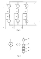
- Fig. 1 shows a three-phase converter known in the art.
- the three phase legs 1, 2 and 3 of the device of Fig. 1 each comprise two so-called arms in series-connection: a positive, upper arm which is connected to a first DC terminal 4 at a positive voltage level, and a negative, lower arm, which is connected to a second DC terminal 5 at zero or a negative voltage level.
- Each positive arm comprises a series-connection of an upper voltage source Uvpi and a first passive energy storage element, here in the form of an inductor 9, 11 or 13, respectively, and each negative arm comprises a second passive energy storage element, here also in the form of an inductor 10, 12 or 14, respectively, and a lower voltage source Uvni, where i stands for the number of the corresponding phase leg.
- the midpoint or connection point between the first and second energy storage elements of each phase leg is each connected to an AC terminal 6, 7 or 8, respectively. All the phase legs are connected in parallel to each other and to the two DC terminals 4 and 5.
- each voltage source is made up of a series connected string of submodules 15, where at least two submodules 15 are comprised in one such string.
- the submodules have the form of commutation cells, each cell comprising two valves and a large DC capacitor holding a direct voltage.
- the main valves are equipped with a power electronic switch 16 with turn-off capability and a free-wheeling diode in anti-parallel connection to the switch.
- the corresponding submodule can assume one of two switching states, where in state one zero voltage or in state two the capacitor voltage is applied to the output.
- the converter according to Figs. 1 to 3 is additionally equipped with a passive electronic filter in each phase leg, as is depicted in Fig. 4 for phase leg 1.
- the filter 18 is shown as a dashed box.
- the filter includes three terminals a first terminal for being coupled to the first voltage source and first DC terminal 4, a second terminal for being coupled to the second voltage source and the second DC terminal 5 and finally a third terminal connected to the AC terminal 6 of the converter.
- the first and second passive energy storage elements are being included in the passive filter.
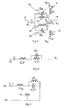
- a first design of the filter 18 is shown fig. 5 .
- This first filter design does, however, not fall within the scope of the present invention.
- a third passive energy storage element 19 in this first design in the form of a capacitor having a capacitance of C p .
- This third passive energy storage element 19 is thus provided in series with the first and second energy storage elements.
- the filter includes two types of passive energy storage elements, inductive and capacitive energy storage elements.
- the third energy storage element 19 is of one of the types, here a capacitive energy storage element, while the fourth and fifth energy storage elements 20 and 21 are of another type, here inductive energy storage elements.
- This first further energy storage element is of another type than the fourth energy storage element and here capacitive with a capacitance C v .
- This second further energy storage element is of another type than the fifth energy storage element and here also capacitive with a capacitance C v . Since the filter includes passive storage elements of the two types, it is clear that filtering is provided in relation to one or more frequencies.
- each path includes a parallel connection of two types of passive energy storage elements.
- the filter has filtering properties in relation to one or more frequencies. This filtering will now be described in more detail.
- the common-mode component u v does not drive any current through the third energy storage element 19, because the potential on each side of this element 19 are affected equally by this component. This allows this element to be removed when the effect of the common-mode component is considered.
- the circuit in fig. 5 is thus reduced to the two above mentioned paths in parallel and this can be simplified into the equivalent circuit diagram of the common-mode case shown in fig. 6 .
- the capacitance of the parallel connection is thus inversely proportional to the inductance of the parallel connection, where the inverse of the capacitance is equal to a fundamental frequency dependent constant times the inductance. It can also be seen that the constant is the square of the fundamental frequency times a factor that is a multiple of the number 3 and here a multiple of 3 of the number 3 and here also three raised by two.
- the differential-mode component u vc is considered, it can be seen that due to the symmetry, this component does not affect the voltage u f of the AC terminal and therefore not the grid current i v , only the circulating current i c .
- the grid interface i.e. the AC terminal 6
- the two parallel connections made up of the third and first further energy storage elements 20 and 22 and the fourth and second further energy storage elements 21 and 23 are put in series as are the first and second energy storage elements 9 and 10.
- An equivalent circuit for the filter in this differential mode is shown in fig.
- the value of the third energy storage element is inversely proportional to the value of the fourth and fifth energy storage elements.
- the inverse of the value of the third energy storage element is furthermore equal to a fundamental frequency dependent constant times the value of the fourth and fifth energy storage elements, where this constant includes the square of the fundamental frequency times a factor that is a multiple of 2, which multiple is in this case 36. This factor is also a raising of the number two by eight.
- the first filter design which does not fall within the scope of the claims, thus provides a filter, which blocks or reduces the frequencies at two and three times the fundamental frequency. Therefore this component at the two times the fundamental frequency is removed from the circulating currents, which thus reduces the circulating currents.
- the first filter design also removes the component at three times the fundamental frequency, which therefore allows zero sequence third harmonics removal without using a transformer.
- These two types of harmonics component removal further uses some energy storage elements in relation to both components, where the fourth and fifth energy storage elements are here used in this dual way. Because of this dual functionality it is furthermore possible to reduce the size of the third energy storage element. This means that the filter is very economical.
- the filter in fig. 5 Take the filter in fig. 5 as an example.
- the fourth and fifth energy storage elements 20 and 21 with tap changers of a suitably selected number of steps and step sizes.
- the first and second further energy storage elements 22 and 23 variable, for instance through using capacitor banks, the capacitances of which can be modified in suitably selected steps through circuit breakers and/or switching semiconductors.
- the energy storage elements are made adjustable in the way described above there will be provided two parallel variable elements, one in each path from a DC terminal to the AC terminal. It should here be realized that it may be advantageous to have only one such variable energy storage element in the filter, because then the provision of the same variation in relation to the two paths is easier to control.
- An example on this is shown in a second filter design in fig. 8 .
- This second filter design does, however, not fall within the scope of the present invention.
- the only elements that differ from the first filter design are here the third energy storage element and the additional energy storage elements. Otherwise all elements are of the same type and provided in the same position as in the first design.
- the third energy storage element has been split into two energy storage elements 19a and 19b of the same type, i.e. capacitive.
- the second further energy storage element has furthermore been deleted, while the first further energy storage element 22 is adjustable and at a first end connected to a midpoint of the third energy storage element and at a second opposite end connected to the AC terminal 6.
- the midpoint of the third energy storage element is provided as the junction between the two energy storage elements 19a and 19b resulting from the splitting.
- This filter functions in the same way as the filter according to the first design, but the filter values can be adjusted and here through adjusting only one energy storage element. However, the selection of capacitor values C v and C p will differ from in the first design.
- the converter without a transformer.
- a transformer is then not only used for removing zero sequence third harmonics. It also acts as a DC blocking element, i.e. it stops DC components appearing in a phase leg from reaching the AC grid. If no transformer is used these DC components will have to be removed or blocked in another way.
- the filter acts, in addition to reducing harmonics at two and three times the fundamental frequency, also as a DC blocking filter.
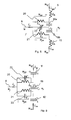
- FIG. 9 thus shows a filter according to a first embodiment of the invention having a first 9', second 10', third 19, fourth 20, fifth 21, first further 22 and second further 23 energy storage element in the same positions as the corresponding elements in the first filter design.
- the third, fourth, fifth, first further and second further energy storage elements are the same elements of the same types at the same positions as in the first design and shown in fig. 5 .
- the first and second energy storage elements 9' and 10' are capacitive and not inductive. There are furthermore no inductive or restive elements in parallel with them. They will therefore stop any DC component appearing in the phase leg from reaching the AC terminal.
- FIG. 10 Another variation providing the three functions is shown in fig. 10 .
- fig. 10 there is shown a filter according to a second embodiment of the invention.
- This filter includes the first and second energy storage elements 9, 10 of the first filter design. They are thus of the same type and placed at the same position as in fig. 5 .
- the third, fourth and fifth energy storage elements 19'. 20' and 21' are of the opposite type compared to the first design.
- the third energy storage element is inductive having an inductance L p
- the fourth and fifth energy storage elements are capacitive having capacitances C v .
- the further energy storage elements 25 and 26 are here capactive with capacitance C p and provided in parallel with the first and second energy storage elements 9 and 10.
- the filter here includes two parallel connections of the two types of elements, inductive and capacitive, through the first and second energy storage elements 9 and 10 being connected in parallel with a respective further element 25 and 26 of the opposite type. These parallel connections here provide the third harmonics filtering.
- the second harmonics filtering is again performed by the third, fourth and fifth energy storage elements.
- the fourth and fifth energy storage elements 20' and 21' also have the additional function of providing DC blocking.
- the selection of capacitor values C v and C p thus differs from in the first filter design.
- FIG. 11 Another variation providing the three functions is shown in fig. 11 .
- fig. 11 there is shown a filter according to a third design, which does not fall within the scope of the claims.
- This filter is based on the filter according to the first filter design.
- This filter therefore includes the first, second, third, fourth, fifth, first further and second further energy storage elements 9, 10, 19, 20, 21, 22 and 23 of the first filter design.
- the filter thus includes the same elements of the same types at the same positions as in fig. 5 .
- the filter includes a sixth passive energy storage element 27 that is capacitive and at one end connected to both the second ends of the fourth and the fifth energy storage elements 20 and 21 and at a second end connected to the AC terminal 6.
- This sixth passive energy storage element 27 thus functions as the DC blocking element and has a capacitance C DBC .
- FIG. 12 Yet another variation according to a fourth design, which does not fall within the scope of the claims, is shown in fig. 12 .
- This variation is based on the second filter design. It thus has the same elements of the same types and provided at the same positions as in fig. 8 . In addition to this it also has the same type of DC blocking element as in the third filter design, i.e. a DC blocking element 27 placed at the same position in relation to the rest of the filter elements as in fig. 11 . Since the fourth filter design is based on the second filter design, the selection of capacitor values C v and C p will differ from the first filter design.
- This filter is based on the filter according to the second embodiment. It includes the first, second, third, fourth and fifth energy storage elements 9, 10, 19', 20' and 21' in the same way as in the second embodiment. These filter elements are thus of the same types at the same positions as in fig. 10 , where the third, fourth sand fifth elements provide frequency component reduction at twice the fundamental frequency and the fourth and fifth elements also provide DC blocking.
- the filter here additionally includes only one parallel connection of the two types of elements, inductive and capacitive, in the paths between the DC terminals and the AC terminal, through providing an additional parallel connection of inductor 28 with inductance L 3h and capacitor 29 with capacitance C 3h .
- This additional parallel connection is here provided in series between the AC terminal 6 and a junction between the parallel fourth and fifth energy storage elements 20' and 21'.
- the selection of capacitor values C v and C p will also here differ from the first filter design.
- the invention has a number of advantages. It blocks circulating currents without having to resort to removing the current through the control of the voltage sources. This is combined with removal of zero sequence third harmonics. In this way no transformer is needed.
- some filter element may be involved in both types of filtering. There may thus be a dual use of a filter element. This reduces the amount of filter elements needed and also allows a size reduction of such a filter element compared with a filter only filtering at twice the fundamental frequency. This is combined with stopping a DC component from reaching the grid, which is also of advantage if there is no transformer between grid and voltage source converter.
- a filter element may combine DC blocking with a frequency filtering function, which provides even further savings.
Landscapes
- Engineering & Computer Science (AREA)
- Power Engineering (AREA)
- Inverter Devices (AREA)
- Supply And Distribution Of Alternating Current (AREA)
Claims (17)
- Vorrichtung zum Umwandeln einer Gleichspannung in eine Wechselspannung und umgekehrt, die mindestens einen Phasenzweig (1, 2, 3) umfasst, wobei jeder Phasenzweig eine erste Spannungsquelle (Uvp1, Uvp2, Uvp3) und ein erstes passives Energiespeicherelement (9, 11, 13; 9'), die zwischen einem ersten Gleichspannungsanschluss (4) und einem ersten Wechselspannungsanschluss (6) in Reihe geschaltet sind, und ein zweites passives Energiespeicherelement (10, 12, 14; 10') und eine zweite Spannungsquelle (Uvn1, Uvn2, Uvn3), die zwischen dem ersten Wechselspannungsanschluss (5) und einem zweiten Gleichspannungsanschluss (6) in Reihe geschaltet sind, aufweist, wobei jede der Spannungsquellen mindestens ein erstes und ein zweites Untermodul (15) in einer Reihenschaltung umfasst, wobei jedes Untermodul (15) mindestens zwei elektronische Schalter (16) umfasst, die mit mindestens einem Kondensator (17) parallel geschaltet sind, und ein passives elektronisches Filter (18), das passive Energiespeicherelemente umfasst, ebenso wie der erste Wechselspannungsanschluss zwischen der ersten und der zweiten Spannungsquelle angeordnet ist, wobei das Filter das erste und das zweite Energiespeicherelement, ein drittes Energiespeicherelement (19; 19'; 19a; 19b), das zwischen dem ersten und dem zweiten Energiespeicherelement in Reihe geschaltet ist, ein viertes Energiespeicherelement (20; 20') mit zwei Enden, wobei ein erstes Ende mit einer Verbindung zwischen dem ersten Energiespeicherelement und dem dritten Energiespeicherelement verbunden ist und ein zweites Ende an den Wechselspannungsanschluss gekoppelt ist, und ein fünftes Energiespeicherelement (21; 21') mit zwei Enden, wobei ein erstes Ende mit einer Verbindung zwischen dem zweiten Energiespeicherelement und dem dritten Energiespeicherelement verbunden ist und ein zweites Ende an den Wechselspannungsanschluss gekoppelt ist, umfasst, wobei die Energiespeicherelemente Elemente von zwei unterschiedlichen Typen umfassen, nämlich kapazitive und induktive Energiespeicherelemente, mit Werten, die ausgewählt sind, um eine Verminderung der Frequenzkomponenten auf das Dreifache der Grundfrequenz der Wechselspannung bereitzustellen,
dadurch gekennzeichnet, dass
die Energiespeicherelemente Elemente mit Werten umfassen, die ausgewählt sind, um eine Verminderung der Frequenzkomponenten auf das Zweifache der Grundfrequenz der Wechselspannung bereitzustellen, und
mindestens ein kapazitives Element (20', 21'; 9', 10'; 27) des Filters ein Gleichspannungs-Sperrelement ist, um die Gleichspannungskomponenten von einem Erreichen des Wechselspannungsanschlusses abzuhalten. - Vorrichtung nach Anspruch 1, wobei das dritte Energiespeicherelement von einem Typ und das vierte und das fünfte Energiespeicherelement von einem anderen Typ sind.
- Vorrichtung nach Anspruch 1 oder 2, wobei die Energiespeicherelemente, die ein Filtern auf das Dreifache der Grundfrequenz bereitstellen, mindestens eine Parallelschaltung der zwei Typen von Elementen enthalten, wobei jeder Weg zwischen den Gleichspannungsanschlüssen und den Wechselspannungsanschlüssen eine solche Parallelschaltung enthält.
- Vorrichtung nach Anspruch 3, wobei solche Parallelschaltungen durch das erste und das zweite Energiespeicherelement bereitgestellt werden, die mit jeweils einem weiteren Element (25, 26) des entgegengesetzten Typs parallel geschaltet sind, um zwei Parallelschaltungen bereitzustellen.
- Vorrichtung nach Anspruch 3, wobei mindestens eines der Elemente (20, 21) des Filters ein kombiniertes Filterelement ist, das das Filtern sowohl auf das Zweifache als auch auf das Dreifache der Grundfrequenz der Wechselspannung unterstützt.
- Vorrichtung nach Anspruch 5, wobei solche Parallelschaltungen durch mindestens ein weiteres Energiespeicherelement (22) bereitgestellt werden, das von einem anderen Typ als das vierte und das fünfte Energiespeicherelement ist und das in einem Zweig verbunden ist, der zu dem vierten Energiespeicherelement parallel geschaltet ist.
- Vorrichtung nach Anspruch 6, wobei das weitere Element (22) auch in einem Zweig angeschlossen ist, der zu dem fünften Element parallel ist, und das mit dem Mittelpunkt des dritten Energiespeicherelements (19a, 19b) verbunden ist.
- Vorrichtung nach Anspruch 6, wobei ein erstes weiteres Element (22), das zu dem vierten Element parallel ist, und ein zweites weiteres Element (23), das zu dem fünften Element parallel ist, bereitgestellt sind.
- Vorrichtung nach einem der Ansprüche 3 bis 8, wobei der Wert von einem Energiespeicherelement von einer solchen Parallelschaltung zu dem Wert des anderen Energiespeicherelements der Parallelschaltung umgekehrt proportional ist, wobei der umgekehrte Wert des einen Speicherelements gleich einer Grundfrequenz ist und von dem konstanten Vielfachen des Werts des anderen Energiespeicherelements abhängig ist.
- Vorrichtung nach Anspruch 9, wobei die Konstante das Quadrat der Grundfrequenz mal einen Faktor ist, der ein Vielfaches von 3 ist.
- Vorrichtung nach einem vorhergehenden Anspruch, wobei das dritte, das vierte und das fünfte Energiespeicherelement in einem Filterabschnitt vorgesehen sind, der ein Filtern auf das Zweifache der Grundfrequenz der Wechselspannung bereitstellt.
- Vorrichtung nach Anspruch 11, wobei der Wert des dritten Energiespeicherelements zu dem Wert des vierten und des fünften Energiespeicherelements umgekehrt proportional ist, wobei der umgekehrte Wert des dritten Energiespeicherelements gleich einer Grundfrequenz ist und von dem konstanten Vielfachen des Werts des vierten und des fünften Energiespeicherelements abhängig ist.
- Vorrichtung nach Anspruch 12, wobei die Konstante das Quadrat der Grundfrequenz mal einen Faktor ist, der eine Abhängigkeit von einem Vielfachen von 2 aufweist.
- Vorrichtung nach einem vorhergehenden Anspruch, wobei mindestens eines der Elemente, das ein Filtern auf das Zweifache der Grundfrequenz bereitstellt, anpassbar ist.
- Vorrichtung nach einem vorhergehenden Anspruch, wobei mindestens eines der passiven Energiespeicherelemente des Filters ein kombiniertes Gleichspannungs-Sperrelement und Frequenzfilterelement auf das Zweifache der Grundfrequenz ist.
- Vorrichtung nach Anspruch 15, wobei das vierte und das fünfte Energiespeicherelement (20', 21') kapazitiv sind und als Gleichspannungs-Sperrelemente arbeiten.
- Vorrichtung nach einem der Ansprüche 1 bis 14, wobei das erste und das zweite Energiespeicherelement (9', 10') kapazitiv sind und als Gleichspannungs-Sperrelemente arbeiten.
Applications Claiming Priority (1)
| Application Number | Priority Date | Filing Date | Title |
|---|---|---|---|
| PCT/EP2010/054997 WO2011127983A1 (en) | 2010-04-15 | 2010-04-15 | Modular multi -level power converter with second and third order harmonics reduction filter |
Publications (2)
| Publication Number | Publication Date |
|---|---|
| EP2559143A1 EP2559143A1 (de) | 2013-02-20 |
| EP2559143B1 true EP2559143B1 (de) | 2014-01-01 |
Family
ID=43661936
Family Applications (1)
| Application Number | Title | Priority Date | Filing Date |
|---|---|---|---|
| EP10713679.8A Active EP2559143B1 (de) | 2010-04-15 | 2010-04-15 | Modularer multilevel umrichter mit sperrfilter für zweite und dritte harmonische |
Country Status (4)
| Country | Link |
|---|---|
| US (1) | US8564981B2 (de) |
| EP (1) | EP2559143B1 (de) |
| CN (1) | CN102823122B (de) |
| WO (1) | WO2011127983A1 (de) |
Families Citing this family (6)
| Publication number | Priority date | Publication date | Assignee | Title |
|---|---|---|---|---|
| DE102012202173B4 (de) | 2012-02-14 | 2013-08-29 | Siemens Aktiengesellschaft | Verfahren zum Betrieb eines mehrphasigen, modularen Multilevelstromrichters |
| US9467111B2 (en) * | 2012-06-29 | 2016-10-11 | Audyssey Laboratories | Operator adjustable full-bandwidth audio spectral shifting control with a simple listener interface |
| CN104283432B (zh) | 2013-07-03 | 2017-12-26 | 通用电气公司 | 联合共模电压注入系统和方法 |
| US9231492B2 (en) * | 2014-01-06 | 2016-01-05 | General Electric Company | System and method of power conversion |
| FR3039940B1 (fr) * | 2015-08-03 | 2017-08-11 | Inst Supergrid | Capacite virtuelle |
| EP3300470A1 (de) * | 2016-09-22 | 2018-03-28 | Siemens Aktiengesellschaft | Umrichter |
Family Cites Families (23)
| Publication number | Priority date | Publication date | Assignee | Title |
|---|---|---|---|---|
| DE1010331B (de) | 1953-06-11 | 1957-06-13 | Kloeckner Humboldt Deutz Ag | Spiralfeder |
| US5210685A (en) * | 1985-03-08 | 1993-05-11 | Westinghouse Electric Corp. | Uninterruptible power supply system and load transfer static switch for such a system |
| US5003455A (en) * | 1990-08-14 | 1991-03-26 | Polyspede Electronics Corporation | Circuitry and method for controlling the firing of a thyristor |
| JP2774685B2 (ja) * | 1990-09-12 | 1998-07-09 | 株式会社東芝 | 3相変圧器の直流偏磁抑制制御を備えたインバータ制御装置 |
| US5414612A (en) * | 1993-08-03 | 1995-05-09 | Asea Brown Boveri Ab | HVDC transmission with a converter connected between an AC voltage and a DC link common to the converters |
| SE520786C2 (sv) * | 1997-03-24 | 2003-08-26 | Abb Ab | Anläggning för överföring av elektrisk effekt |
| US6519169B1 (en) * | 1999-03-29 | 2003-02-11 | Abb Ab | Multiphase inverter with series of connected phase legs |
| DE10103031B4 (de) | 2001-01-24 | 2011-12-01 | Siemens Ag | Stromrichterschaltung mit verteilten Energiespeichern und Verfahren zur Steuerung einer derartigen Stromrichterschaltung |
| DE10217889A1 (de) * | 2002-04-22 | 2003-11-13 | Siemens Ag | Stromversorgung mit einem Direktumrichter |
| SE525546C2 (sv) | 2002-08-16 | 2005-03-08 | Abb Ab | Anläggning för överföring av elektrisk effekt samt ett förfarande för drift av en sådan anläggning |
| GB2397445A (en) | 2003-01-14 | 2004-07-21 | Alstom | Power transmission circuits |
| US7502238B2 (en) * | 2005-03-31 | 2009-03-10 | Rockwell Automation Technologies, Inc. | Rectifier for reducing current harmonics from unbalanced source |
| JP4811917B2 (ja) * | 2005-12-27 | 2011-11-09 | 三菱電機株式会社 | 電力変換装置 |
| US7485987B2 (en) * | 2006-02-23 | 2009-02-03 | Mitsubishi Denki Kabushiki Kaisha | Power converting device |
| ATE523950T1 (de) | 2006-12-08 | 2011-09-15 | Siemens Ag | Vorrichtung zum umrichten eines elektrischen stromes |
| US7848121B2 (en) * | 2007-05-14 | 2010-12-07 | Honeywell International Inc. | Advanced matrix converter and method for operation |
| US8345457B2 (en) * | 2007-09-05 | 2013-01-01 | Abb Technology Ag | Voltage source converter for high voltage direct current power transmission |
| US8385097B2 (en) * | 2008-01-08 | 2013-02-26 | Abb Technology Ag | Method for controlling a voltage source converter and a voltage converting apparatus |
| BRPI0822496A2 (pt) * | 2008-03-20 | 2015-06-16 | Abb Res Ag | Conversor de fonte de voltagem |
| JP2009273355A (ja) * | 2008-05-06 | 2009-11-19 | Siemens Ag | 電力伝送のための装置 |
| US8665617B2 (en) * | 2008-06-12 | 2014-03-04 | Abb Technology Ag | Plant for transmitting electric power |
| CN102224669B (zh) * | 2008-11-21 | 2014-04-16 | Abb技术有限公司 | 具有多电平电压输出和谐波滤波器的功率转换器 |
| WO2011141059A1 (en) * | 2010-05-11 | 2011-11-17 | Abb Research Ltd | An ac/dc converter |
-
2010
- 2010-04-15 EP EP10713679.8A patent/EP2559143B1/de active Active
- 2010-04-15 WO PCT/EP2010/054997 patent/WO2011127983A1/en not_active Ceased
- 2010-04-15 CN CN201080066177.1A patent/CN102823122B/zh active Active
- 2010-04-15 US US13/641,380 patent/US8564981B2/en active Active
Also Published As
| Publication number | Publication date |
|---|---|
| CN102823122A (zh) | 2012-12-12 |
| WO2011127983A1 (en) | 2011-10-20 |
| US8564981B2 (en) | 2013-10-22 |
| EP2559143A1 (de) | 2013-02-20 |
| US20130027995A1 (en) | 2013-01-31 |
| CN102823122B (zh) | 2016-01-20 |
Similar Documents
| Publication | Publication Date | Title |
|---|---|---|
| Saeedian et al. | Step‐up switched‐capacitor module for cascaded MLI topologies | |
| Norrga et al. | The polyphase cascaded-cell DC/DC converter | |
| KR101292991B1 (ko) | 멀티레벨 전압 출력 및 고조파 보상기를 갖는 전력 변환기 | |
| US8665617B2 (en) | Plant for transmitting electric power | |
| US8564981B2 (en) | Modular multi-level power converter with second and third order harmonics reduction filter | |
| US8553435B2 (en) | Power converter with multi-level voltage output and harmonics filter | |
| CA2565707C (en) | Low harmonics, polyphase converter circuit | |
| DE102010008426A1 (de) | 3-Stufen-Pulswechselrichter mit Entlastungsnetzwerk | |
| Huber et al. | Common-mode currents in multi-cell solid-state transformers | |
| Li et al. | Magnetic integration of LTL filter with two LC-traps for grid-connected power converters | |
| Ismeil | High dynamic performance for split-source inverter based on finite control set model predictive control | |
| Büyük et al. | Analysis and comparison of passive damping methods for shunt active power filter with output LCL filter | |
| Khowja et al. | Integrated output filter inductor for permanent magnet motor drives | |
| WO2011127984A1 (en) | Modular multi -level power converter with harmonics reduction and dc blocking filter | |
| KR102952122B1 (ko) | 트랜스포머 배열체 및 전압 변환 방법 | |
| Parida et al. | A new modular multilevel converter circuit topology with reduced number of power cells for DC to AC applications | |
| Almaguer et al. | A frequency-based LCL filter design and control considerations for three-phase converters for solid-state transformer applications | |
| Naresh et al. | Comparison of passive damping based LCL filter design methods for grid-connected voltage source converters | |
| Acharya et al. | Stability analysis of a medium voltage cascaded converter system with reduced DC-link capacitance | |
| JP2016226224A (ja) | モジュラーマルチレベル変換器 | |
| Udovichenko | AC voltage regulators with high frequency transformer review | |
| Jacobs et al. | Multi-phase series resonant dc-to-dc converters: Transient investigations | |
| Wang et al. | Performance evaluation of a two-terminal active Inductor in the DC-link filter of a three-phase diode bridge rectifier | |
| WO2012003857A1 (en) | Interface arrangement between ac and dc systems | |
| Franke et al. | Analysis of control strategies for a 3 phase 4 wire topology for transformerless solar inverters |
Legal Events
| Date | Code | Title | Description |
|---|---|---|---|
| PUAI | Public reference made under article 153(3) epc to a published international application that has entered the european phase |
Free format text: ORIGINAL CODE: 0009012 |
|
| 17P | Request for examination filed |
Effective date: 20121115 |
|
| AK | Designated contracting states |
Kind code of ref document: A1 Designated state(s): AT BE BG CH CY CZ DE DK EE ES FI FR GB GR HR HU IE IS IT LI LT LU LV MC MK MT NL NO PL PT RO SE SI SK SM TR |
|
| RIN1 | Information on inventor provided before grant (corrected) |
Inventor name: HARNEFORS, LENNART Inventor name: SHUKLA, ANSHUMAN DEPARTMENT OF ELECTRICAL ENGINEER Inventor name: NORRGA, STAFFAN |
|
| DAX | Request for extension of the european patent (deleted) | ||
| GRAP | Despatch of communication of intention to grant a patent |
Free format text: ORIGINAL CODE: EPIDOSNIGR1 |
|
| INTG | Intention to grant announced |
Effective date: 20131008 |
|
| GRAS | Grant fee paid |
Free format text: ORIGINAL CODE: EPIDOSNIGR3 |
|
| GRAA | (expected) grant |
Free format text: ORIGINAL CODE: 0009210 |
|
| AK | Designated contracting states |
Kind code of ref document: B1 Designated state(s): AT BE BG CH CY CZ DE DK EE ES FI FR GB GR HR HU IE IS IT LI LT LU LV MC MK MT NL NO PL PT RO SE SI SK SM TR |
|
| REG | Reference to a national code |
Ref country code: GB Ref legal event code: FG4D |
|
| REG | Reference to a national code |
Ref country code: CH Ref legal event code: EP |
|
| REG | Reference to a national code |
Ref country code: IE Ref legal event code: FG4D |
|
| REG | Reference to a national code |
Ref country code: AT Ref legal event code: REF Ref document number: 647975 Country of ref document: AT Kind code of ref document: T Effective date: 20140215 |
|
| REG | Reference to a national code |
Ref country code: DE Ref legal event code: R096 Ref document number: 602010012820 Country of ref document: DE Effective date: 20140220 |
|
| REG | Reference to a national code |
Ref country code: SE Ref legal event code: TRGR |
|
| REG | Reference to a national code |
Ref country code: NL Ref legal event code: VDEP Effective date: 20140101 |
|
| REG | Reference to a national code |
Ref country code: AT Ref legal event code: MK05 Ref document number: 647975 Country of ref document: AT Kind code of ref document: T Effective date: 20140101 |
|
| REG | Reference to a national code |
Ref country code: LT Ref legal event code: MG4D |
|
| PG25 | Lapsed in a contracting state [announced via postgrant information from national office to epo] |
Ref country code: LT Free format text: LAPSE BECAUSE OF FAILURE TO SUBMIT A TRANSLATION OF THE DESCRIPTION OR TO PAY THE FEE WITHIN THE PRESCRIBED TIME-LIMIT Effective date: 20140101 Ref country code: IS Free format text: LAPSE BECAUSE OF FAILURE TO SUBMIT A TRANSLATION OF THE DESCRIPTION OR TO PAY THE FEE WITHIN THE PRESCRIBED TIME-LIMIT Effective date: 20140501 |
|
| PG25 | Lapsed in a contracting state [announced via postgrant information from national office to epo] |
Ref country code: PT Free format text: LAPSE BECAUSE OF FAILURE TO SUBMIT A TRANSLATION OF THE DESCRIPTION OR TO PAY THE FEE WITHIN THE PRESCRIBED TIME-LIMIT Effective date: 20140502 Ref country code: FI Free format text: LAPSE BECAUSE OF FAILURE TO SUBMIT A TRANSLATION OF THE DESCRIPTION OR TO PAY THE FEE WITHIN THE PRESCRIBED TIME-LIMIT Effective date: 20140101 Ref country code: ES Free format text: LAPSE BECAUSE OF FAILURE TO SUBMIT A TRANSLATION OF THE DESCRIPTION OR TO PAY THE FEE WITHIN THE PRESCRIBED TIME-LIMIT Effective date: 20140101 Ref country code: NL Free format text: LAPSE BECAUSE OF FAILURE TO SUBMIT A TRANSLATION OF THE DESCRIPTION OR TO PAY THE FEE WITHIN THE PRESCRIBED TIME-LIMIT Effective date: 20140101 Ref country code: CY Free format text: LAPSE BECAUSE OF FAILURE TO SUBMIT A TRANSLATION OF THE DESCRIPTION OR TO PAY THE FEE WITHIN THE PRESCRIBED TIME-LIMIT Effective date: 20140101 Ref country code: AT Free format text: LAPSE BECAUSE OF FAILURE TO SUBMIT A TRANSLATION OF THE DESCRIPTION OR TO PAY THE FEE WITHIN THE PRESCRIBED TIME-LIMIT Effective date: 20140101 |
|
| PG25 | Lapsed in a contracting state [announced via postgrant information from national office to epo] |
Ref country code: LV Free format text: LAPSE BECAUSE OF FAILURE TO SUBMIT A TRANSLATION OF THE DESCRIPTION OR TO PAY THE FEE WITHIN THE PRESCRIBED TIME-LIMIT Effective date: 20140101 Ref country code: HR Free format text: LAPSE BECAUSE OF FAILURE TO SUBMIT A TRANSLATION OF THE DESCRIPTION OR TO PAY THE FEE WITHIN THE PRESCRIBED TIME-LIMIT Effective date: 20140101 Ref country code: BE Free format text: LAPSE BECAUSE OF FAILURE TO SUBMIT A TRANSLATION OF THE DESCRIPTION OR TO PAY THE FEE WITHIN THE PRESCRIBED TIME-LIMIT Effective date: 20140101 |
|
| REG | Reference to a national code |
Ref country code: DE Ref legal event code: R097 Ref document number: 602010012820 Country of ref document: DE |
|
| PG25 | Lapsed in a contracting state [announced via postgrant information from national office to epo] |
Ref country code: EE Free format text: LAPSE BECAUSE OF FAILURE TO SUBMIT A TRANSLATION OF THE DESCRIPTION OR TO PAY THE FEE WITHIN THE PRESCRIBED TIME-LIMIT Effective date: 20140101 Ref country code: RO Free format text: LAPSE BECAUSE OF FAILURE TO SUBMIT A TRANSLATION OF THE DESCRIPTION OR TO PAY THE FEE WITHIN THE PRESCRIBED TIME-LIMIT Effective date: 20140101 Ref country code: DK Free format text: LAPSE BECAUSE OF FAILURE TO SUBMIT A TRANSLATION OF THE DESCRIPTION OR TO PAY THE FEE WITHIN THE PRESCRIBED TIME-LIMIT Effective date: 20140101 Ref country code: CZ Free format text: LAPSE BECAUSE OF FAILURE TO SUBMIT A TRANSLATION OF THE DESCRIPTION OR TO PAY THE FEE WITHIN THE PRESCRIBED TIME-LIMIT Effective date: 20140101 |
|
| PLBE | No opposition filed within time limit |
Free format text: ORIGINAL CODE: 0009261 |
|
| STAA | Information on the status of an ep patent application or granted ep patent |
Free format text: STATUS: NO OPPOSITION FILED WITHIN TIME LIMIT |
|
| PG25 | Lapsed in a contracting state [announced via postgrant information from national office to epo] |
Ref country code: MC Free format text: LAPSE BECAUSE OF FAILURE TO SUBMIT A TRANSLATION OF THE DESCRIPTION OR TO PAY THE FEE WITHIN THE PRESCRIBED TIME-LIMIT Effective date: 20140101 Ref country code: PL Free format text: LAPSE BECAUSE OF FAILURE TO SUBMIT A TRANSLATION OF THE DESCRIPTION OR TO PAY THE FEE WITHIN THE PRESCRIBED TIME-LIMIT Effective date: 20140101 Ref country code: SK Free format text: LAPSE BECAUSE OF FAILURE TO SUBMIT A TRANSLATION OF THE DESCRIPTION OR TO PAY THE FEE WITHIN THE PRESCRIBED TIME-LIMIT Effective date: 20140101 Ref country code: LU Free format text: LAPSE BECAUSE OF FAILURE TO SUBMIT A TRANSLATION OF THE DESCRIPTION OR TO PAY THE FEE WITHIN THE PRESCRIBED TIME-LIMIT Effective date: 20140415 |
|
| REG | Reference to a national code |
Ref country code: CH Ref legal event code: PL |
|
| 26N | No opposition filed |
Effective date: 20141002 |
|
| REG | Reference to a national code |
Ref country code: DE Ref legal event code: R097 Ref document number: 602010012820 Country of ref document: DE Effective date: 20141002 |
|
| REG | Reference to a national code |
Ref country code: IE Ref legal event code: MM4A |
|
| PG25 | Lapsed in a contracting state [announced via postgrant information from national office to epo] |
Ref country code: LI Free format text: LAPSE BECAUSE OF NON-PAYMENT OF DUE FEES Effective date: 20140430 Ref country code: CH Free format text: LAPSE BECAUSE OF NON-PAYMENT OF DUE FEES Effective date: 20140430 |
|
| PG25 | Lapsed in a contracting state [announced via postgrant information from national office to epo] |
Ref country code: IE Free format text: LAPSE BECAUSE OF NON-PAYMENT OF DUE FEES Effective date: 20140415 |
|
| PG25 | Lapsed in a contracting state [announced via postgrant information from national office to epo] |
Ref country code: SI Free format text: LAPSE BECAUSE OF FAILURE TO SUBMIT A TRANSLATION OF THE DESCRIPTION OR TO PAY THE FEE WITHIN THE PRESCRIBED TIME-LIMIT Effective date: 20140101 |
|
| PG25 | Lapsed in a contracting state [announced via postgrant information from national office to epo] |
Ref country code: MT Free format text: LAPSE BECAUSE OF FAILURE TO SUBMIT A TRANSLATION OF THE DESCRIPTION OR TO PAY THE FEE WITHIN THE PRESCRIBED TIME-LIMIT Effective date: 20140101 |
|
| REG | Reference to a national code |
Ref country code: FR Ref legal event code: PLFP Year of fee payment: 7 |
|
| PG25 | Lapsed in a contracting state [announced via postgrant information from national office to epo] |
Ref country code: NO Free format text: LAPSE BECAUSE OF FAILURE TO SUBMIT A TRANSLATION OF THE DESCRIPTION OR TO PAY THE FEE WITHIN THE PRESCRIBED TIME-LIMIT Effective date: 20140401 Ref country code: SM Free format text: LAPSE BECAUSE OF FAILURE TO SUBMIT A TRANSLATION OF THE DESCRIPTION OR TO PAY THE FEE WITHIN THE PRESCRIBED TIME-LIMIT Effective date: 20140101 |
|
| PG25 | Lapsed in a contracting state [announced via postgrant information from national office to epo] |
Ref country code: IT Free format text: LAPSE BECAUSE OF FAILURE TO SUBMIT A TRANSLATION OF THE DESCRIPTION OR TO PAY THE FEE WITHIN THE PRESCRIBED TIME-LIMIT Effective date: 20140101 Ref country code: BG Free format text: LAPSE BECAUSE OF FAILURE TO SUBMIT A TRANSLATION OF THE DESCRIPTION OR TO PAY THE FEE WITHIN THE PRESCRIBED TIME-LIMIT Effective date: 20140101 Ref country code: GR Free format text: LAPSE BECAUSE OF FAILURE TO SUBMIT A TRANSLATION OF THE DESCRIPTION OR TO PAY THE FEE WITHIN THE PRESCRIBED TIME-LIMIT Effective date: 20140402 |
|
| PG25 | Lapsed in a contracting state [announced via postgrant information from national office to epo] |
Ref country code: TR Free format text: LAPSE BECAUSE OF FAILURE TO SUBMIT A TRANSLATION OF THE DESCRIPTION OR TO PAY THE FEE WITHIN THE PRESCRIBED TIME-LIMIT Effective date: 20140101 Ref country code: HU Free format text: LAPSE BECAUSE OF FAILURE TO SUBMIT A TRANSLATION OF THE DESCRIPTION OR TO PAY THE FEE WITHIN THE PRESCRIBED TIME-LIMIT; INVALID AB INITIO Effective date: 20100415 |
|
| REG | Reference to a national code |
Ref country code: FR Ref legal event code: PLFP Year of fee payment: 8 |
|
| REG | Reference to a national code |
Ref country code: FR Ref legal event code: PLFP Year of fee payment: 9 |
|
| PG25 | Lapsed in a contracting state [announced via postgrant information from national office to epo] |
Ref country code: MK Free format text: LAPSE BECAUSE OF FAILURE TO SUBMIT A TRANSLATION OF THE DESCRIPTION OR TO PAY THE FEE WITHIN THE PRESCRIBED TIME-LIMIT Effective date: 20140101 |
|
| REG | Reference to a national code |
Ref country code: DE Ref legal event code: R084 Ref document number: 602010012820 Country of ref document: DE |
|
| REG | Reference to a national code |
Ref country code: DE Ref legal event code: R081 Ref document number: 602010012820 Country of ref document: DE Owner name: HITACHI ENERGY SWITZERLAND AG, CH Free format text: FORMER OWNER: ABB RESEARCH LTD., ZUERICH, CH Ref country code: DE Ref legal event code: R082 Ref document number: 602010012820 Country of ref document: DE Representative=s name: MUELLER, ANDREAS, DIPL.-PHYS. DR. RER. NAT., DE Ref country code: DE Ref legal event code: R081 Ref document number: 602010012820 Country of ref document: DE Owner name: ABB SCHWEIZ AG, CH Free format text: FORMER OWNER: ABB RESEARCH LTD., ZUERICH, CH Ref country code: DE Ref legal event code: R081 Ref document number: 602010012820 Country of ref document: DE Owner name: ABB POWER GRIDS SWITZERLAND AG, CH Free format text: FORMER OWNER: ABB RESEARCH LTD., ZUERICH, CH Ref country code: DE Ref legal event code: R082 Ref document number: 602010012820 Country of ref document: DE Representative=s name: DENNEMEYER & ASSOCIATES S.A., DE |
|
| REG | Reference to a national code |
Ref country code: GB Ref legal event code: 732E Free format text: REGISTERED BETWEEN 20200206 AND 20200212 |
|
| REG | Reference to a national code |
Ref country code: DE Ref legal event code: R081 Ref document number: 602010012820 Country of ref document: DE Owner name: HITACHI ENERGY SWITZERLAND AG, CH Free format text: FORMER OWNER: ABB SCHWEIZ AG, BADEN, CH Ref country code: DE Ref legal event code: R082 Ref document number: 602010012820 Country of ref document: DE Representative=s name: DENNEMEYER & ASSOCIATES RECHTSANWALTSGESELLSCH, DE Ref country code: DE Ref legal event code: R081 Ref document number: 602010012820 Country of ref document: DE Owner name: HITACHI ENERGY LTD, CH Free format text: FORMER OWNER: ABB SCHWEIZ AG, BADEN, CH Ref country code: DE Ref legal event code: R082 Ref document number: 602010012820 Country of ref document: DE Representative=s name: DENNEMEYER & ASSOCIATES S.A., DE Ref country code: DE Ref legal event code: R081 Ref document number: 602010012820 Country of ref document: DE Owner name: ABB POWER GRIDS SWITZERLAND AG, CH Free format text: FORMER OWNER: ABB SCHWEIZ AG, BADEN, CH |
|
| REG | Reference to a national code |
Ref country code: GB Ref legal event code: 732E Free format text: REGISTERED BETWEEN 20211104 AND 20211110 |
|
| REG | Reference to a national code |
Ref country code: DE Ref legal event code: R081 Ref document number: 602010012820 Country of ref document: DE Owner name: HITACHI ENERGY SWITZERLAND AG, CH Free format text: FORMER OWNER: ABB POWER GRIDS SWITZERLAND AG, BADEN, CH Ref country code: DE Ref legal event code: R081 Ref document number: 602010012820 Country of ref document: DE Owner name: HITACHI ENERGY LTD, CH Free format text: FORMER OWNER: ABB POWER GRIDS SWITZERLAND AG, BADEN, CH |
|
| P01 | Opt-out of the competence of the unified patent court (upc) registered |
Effective date: 20230527 |
|
| REG | Reference to a national code |
Ref country code: DE Ref legal event code: R082 Ref document number: 602010012820 Country of ref document: DE Representative=s name: DENNEMEYER & ASSOCIATES RECHTSANWALTSGESELLSCH, DE Ref country code: DE Ref legal event code: R082 Ref document number: 602010012820 Country of ref document: DE Representative=s name: DENNEMEYER & ASSOCIATES S.A., DE Ref country code: DE Ref legal event code: R081 Ref document number: 602010012820 Country of ref document: DE Owner name: HITACHI ENERGY LTD, CH Free format text: FORMER OWNER: HITACHI ENERGY SWITZERLAND AG, BADEN, CH |
|
| REG | Reference to a national code |
Ref country code: GB Ref legal event code: 732E Free format text: REGISTERED BETWEEN 20240718 AND 20240724 |
|
| REG | Reference to a national code |
Ref country code: DE Ref legal event code: R082 Ref document number: 602010012820 Country of ref document: DE Representative=s name: DENNEMEYER & ASSOCIATES RECHTSANWALTSGESELLSCH, DE |
|
| PGFP | Annual fee paid to national office [announced via postgrant information from national office to epo] |
Ref country code: GB Payment date: 20260423 Year of fee payment: 17 |
|
| PGFP | Annual fee paid to national office [announced via postgrant information from national office to epo] |
Ref country code: DE Payment date: 20260422 Year of fee payment: 17 |
|
| PGFP | Annual fee paid to national office [announced via postgrant information from national office to epo] |
Ref country code: SE Payment date: 20260420 Year of fee payment: 17 |
|
| PGFP | Annual fee paid to national office [announced via postgrant information from national office to epo] |
Ref country code: FR Payment date: 20260420 Year of fee payment: 17 |