EP2560080A1 - Système tactile optique et procédé de positionnement associé - Google Patents
Système tactile optique et procédé de positionnement associé Download PDFInfo
- Publication number
- EP2560080A1 EP2560080A1 EP12172711A EP12172711A EP2560080A1 EP 2560080 A1 EP2560080 A1 EP 2560080A1 EP 12172711 A EP12172711 A EP 12172711A EP 12172711 A EP12172711 A EP 12172711A EP 2560080 A1 EP2560080 A1 EP 2560080A1
- Authority
- EP
- European Patent Office
- Prior art keywords
- optical touch
- touch system
- image sensors
- sensors
- image
- Prior art date
- Legal status (The legal status is an assumption and is not a legal conclusion. Google has not performed a legal analysis and makes no representation as to the accuracy of the status listed.)
- Withdrawn
Links
Images


Classifications
-
- G—PHYSICS
- G06—COMPUTING OR CALCULATING; COUNTING
- G06F—ELECTRIC DIGITAL DATA PROCESSING
- G06F3/00—Input arrangements for transferring data to be processed into a form capable of being handled by the computer; Output arrangements for transferring data from processing unit to output unit, e.g. interface arrangements
- G06F3/01—Input arrangements or combined input and output arrangements for interaction between user and computer
- G06F3/03—Arrangements for converting the position or the displacement of a member into a coded form
- G06F3/041—Digitisers, e.g. for touch screens or touch pads, characterised by the transducing means
- G06F3/0416—Control or interface arrangements specially adapted for digitisers
- G06F3/0418—Control or interface arrangements specially adapted for digitisers for error correction or compensation, e.g. based on parallax, calibration or alignment
-
- G—PHYSICS
- G06—COMPUTING OR CALCULATING; COUNTING
- G06F—ELECTRIC DIGITAL DATA PROCESSING
- G06F3/00—Input arrangements for transferring data to be processed into a form capable of being handled by the computer; Output arrangements for transferring data from processing unit to output unit, e.g. interface arrangements
- G06F3/01—Input arrangements or combined input and output arrangements for interaction between user and computer
- G06F3/03—Arrangements for converting the position or the displacement of a member into a coded form
- G06F3/041—Digitisers, e.g. for touch screens or touch pads, characterised by the transducing means
- G06F3/042—Digitisers, e.g. for touch screens or touch pads, characterised by the transducing means by opto-electronic means
- G06F3/0425—Digitisers, e.g. for touch screens or touch pads, characterised by the transducing means by opto-electronic means using a single imaging device like a video camera for tracking the absolute position of a single or a plurality of objects with respect to an imaged reference surface, e.g. video camera imaging a display or a projection screen, a table or a wall surface, on which a computer generated image is displayed or projected
Definitions
- the present disclosure relates to an optical touch system. More particularly, the present disclosure relates to an optical touch system that adopts a method of adjustable positioning to determine a touch location and positioning method thereof.
- a resistive touch screen comprises of an ITO (Indium-Tin-Oxide) film and a sheet of ITO glass, which are spaced from each other by a plurality of insulation spacers.
- ITO Indium-Tin-Oxide
- a touching object touches and depresses the ITO film, a local depression is formed, which makes contact with the ITO glass located therebelow thereby inducing a variation of voltage, which, after conversion from analog signal to digital signal, is applied to a microprocessor to be processed for calculation and determination of operation position of the touched point.
- Capacitive touch screens determine position coordinates of a touch point based on the capacitance change generated by electrostatic bond between the arranged transparent electrodes and the human body.
- Acoustic-wave touch screens transform electrical signals into ultrasonic waves in advance and then directly transmit to the surface of the touch screen, and when a user touches the screen, the ultrasonic waves are absorbed, which first leads to attenuation and subsequently leads to determination of accurate touch location based on the attenuation amount of the ultrasonic waves before and after touching.
- Resistive touch screens and capacitive touch screens are always mainstreams of the market.
- optical touch technologies are gradually emerging.
- Common optical touch screens can be roughly classified into the following types: infrared type, CMOS/CCD type, embedded type, and projective type touch screens.
- CMOS/CCD type complementary metal-oxide-semiconductor
- embedded type embedded type
- projective type touch screens Typically, optical touch technologies generate a shadow by shading effect and then sense the shadow change by a photosensitive component (such as an image sensor) so as to determine the touch location.
- the image sensor developed on the basis of photoelectric technology, transforms an optical image into one-dimensional time sequence signals.
- Vacuum-tube image sensors include electron-beam camera tubes, image intensifiers and image converters, and examples of semiconductor integrated image sensors are charge coupled devices (CCD) and complementary metal-oxide semiconductor field effect transistors (CMOS) and scanning-type image sensors.
- CCD charge coupled devices
- CMOS complementary metal-oxide semiconductor field effect transistors
- the vacuum-tube image sensors such as electron-beam camera tubes are gradually being replaced by semiconductor integrated image sensors such as CCD and CMOS.
- An object of the present disclosure is to provide an optical touch system and positioning method thereof.
- An optical touch system in the present disclosure comprises an area to be sensed and a sensing unit; the sensing unit comprises at least two image sensors; wherein locations of the image sensors are adjustable and sensing areas of the image sensors intersect with each other forming an intersection zone, further wherein the intersection zone covers the area to be sensed.
- a positioning method of an optical touch system in the present disclosure comprises of: simultaneously driving at least two image sensors ; capturinge image information of an area to be sensed through the two image sensors respectively; analyzing image information to judge whether there are supersaturated responding patches; calculating location information of the area to be sensed corresponding to the supersaturated responding patches ; and getting touch location information of the area to be sensed by calculating location of the center point of the patches composed of the supersaturated pixels.
- An optical touch system and positioning method thereof in the present disclosure is based on stereo vision theory.
- the positioning method comprises adopting at least two adjustable image sensors to capture image information so that it can be applicable to different sizes of touch screens by adjusting locations of the image sensors. Further, sensing area of the touch system covers the whole screen without any need to increase quantity of sensors. Meanwhile, the positioning method, provided in the present disclosure, can make a spectra, emitted by a stylus, correspond to the image sensors so as to reduce touch response time and improve accuracy of touch location detection.
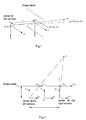
- FIG. 1 is a schematic view 1 of stereo vision theory for an optical touch system.
- FIG. 2 is a schematic view 2 of stereo vision theory for an optical touch system.
- FIG. 3 is a schematic structure view of an optical touch system including a stylus.
- FIG. 4 is a schematic structure view of an adjustable touch system.
- FIG. 5 is a schematic view of mutual spacing adjustment of the adjustable touch system of FIG. 4 .
- FIG. 6 is a schematic structure view of an embedded touch system
- FIG. 7 is a schematic structure view of an external touch system
- FIG. 8 is a sectional view of the connection structure of the external touch system of FIG. 7 ;
- FIG. 9 is a schematic structure view of a stylus which contains IR-LED;
- FIG. 10 is a flowchart of the positioning method for an optical touch system.
- the optical touch system of the present disclosure is based on stereo vision theory.
- stereo vision theory One reason why people have stereo vision is that visual angles of left and right eyes are quite different from each other and an object seen by the left eye is inclined towards the left side and an object seen by the right eye is inclined towards the right side, and the two images, as seen by respective eyes, are transmitted to human brain via an optic nerve. Finally, the two images are integrated into a single stereo image by the brain.
- the present disclosure combines photography principle with stereo vision theory and adopts two image sensors that are equivalent to people's left and right eyes to achieve an accurate positioning of the touch point.
- the main principle of Photography is to record data of a three-dimensional space on a medium of two-dimensional space.
- the medium is a negative film and for digital camera, the medium is each and every pixel on a CMOS sensor.
- the medium When recording information of the three-dimensional space on a medium of two-dimensional space, there is a certain geometrical relationship. Referring to FIG. 1 , for a point P of a three-dimensional space, its coordinates correspond to center of the camera (x c , y c , z c ) and after projecting the point on the image plane through the photography process, its corresponding coordinates become (x i , y i ).
- f is the distance between center of the camera and center of the image plane, and the numerical value of it is known. Therefore, if coordinates of a point P of a three-dimensional space is known, location of its corresponding point on the image plane can be determined based on formulas (1) and (2) given above. On the contrary, if coordinate value of Pi on the image plane is known, it is not possible to back infer the location of point P.
- coordinate of the target point corresponding to the whole photography system is (x c , y c , z c ).
- Coordinate corresponding to the left camera is (x cl , y cl , z cl ) and coordinates of corresponding point on the left image plane is (x il , y il ).
- coordinate corresponding to the right camera is (x cr , y cr , z cr ) and coordinates of corresponding point on the right image plane is (x ir , y ir ).
- an optical touch system 30 at least comprises a first image sensor 31 and a second image sensor 32.
- the distance L between the first image sensor 31 and the second image sensor 32 is also fixed. According to the geometrical relationship of the above formulas (3), (4) and (5), actual touch location can be determined.
- combining the optical touch system 30 which at least comprises of the first image sensor 31 and the second image sensor 32 with a display panel 10 will upgrade the existing non-touch display screen into touch screen.
- the first image sensor 31 and the second image sensor 32 respectively capture images that contain touch location information and then after integrating the two groups of image information by the system, actual touch location information will be calculated and fed back to the display panel 10 so that it can carry out corresponding action.
- sensing scope of the optical touch system is adjustable. Sensing areas of the first image sensor 31 and the second image sensor 32 intersect with each other, forming an intersection zone. In an embodiment, adjusting locations of the image sensors 31 and 32 can make the intersection zone cover the whole area to be sensed. For instance, space between the first image sensor 31 and the second image sensor 32 can be adjusted by an adjustment mechanism 35, as shown in FIG. 5 , to fit different sizes of screens. Wide-angle lenses can also be installed in the image sensors to expand sensing scope. Further, area to be sensed can be the above-mentioned display panel or other screens, such as projection screens. When the size of a screen changes, a user can adjust mutual locations of the image sensors and start a correction program to input new L value into the system; thereby, it can be applied to new touch system.
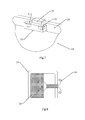
- the optical touch system 30 can adopt embedded type or external type to combine with the display panel 10. If embedded type combination is adopted, as shown in FIG. 6 , the optical touch system 30 can be integrated to the external frame 20 of the display panel 10. On the other hand, if external type combination is adopted, as shown in FIG. 7 , the optical touch system 30 at least comprises a first image sensor 31, a second image sensor 32, and a housing 33, and as shown in FIG. 8 , the housing 33 of the optical touch system 30, and the external frame 20 of the display panel 10 are connected by a fixing screw 34. If the display screen is any other screen such as a projection screen, optical touch system 30 can also be set externally around the screen.
- the optical touch system also comprises a stylus 40, wherein spectra emitted by the stylus 40, corresponding to the image sensors, reduces touch response time and improves accuracy of detection of touch location.
- a stylus 40 wherein spectra emitted by the stylus 40, corresponding to the image sensors, reduces touch response time and improves accuracy of detection of touch location.
- CMOS sensors are adopted as the image sensors
- an IR light source can be set inside a stylus 40. Since CMOS sensors have different responses to the spectra of different wavelengths, especially having a highly sensitive response to IR spectra, when the CMOS sensors capture image information of a touch location, pixels of the corresponding areas on the CMOS sensors are stimulated by IR light and present a state of supersaturated response, which helps in obtaining information of the touch location.
- the stylus 40 at least comprises an on-off switch 42 and an IR LED 41.
- the IR LED 41 can use IR light with the spectrum of 890nm-980nm.
- the stylus 40 operates information input, and when the CMOS sensors capture the image of the IR LED, pixels of the corresponding areas on the sensors are stimulated by the IR light and reach to a state of supersaturated response; and then calculate location of the center point of the patches composed of the supersaturated pixels to get the touch location.
- the method avoids lengthy and complicated image processing process but also improves the speed and accuracy of touch response.
- a positioning method of an optical touch system comprises the following steps:
Landscapes
- Engineering & Computer Science (AREA)
- General Engineering & Computer Science (AREA)
- Theoretical Computer Science (AREA)
- Human Computer Interaction (AREA)
- Physics & Mathematics (AREA)
- General Physics & Mathematics (AREA)
- Multimedia (AREA)
- Position Input By Displaying (AREA)
- Length Measuring Devices By Optical Means (AREA)
Applications Claiming Priority (1)
| Application Number | Priority Date | Filing Date | Title |
|---|---|---|---|
| TW100129704A TWI479390B (zh) | 2011-08-19 | 2011-08-19 | 一種光學式觸控系統及其定位方法 |
Publications (1)
| Publication Number | Publication Date |
|---|---|
| EP2560080A1 true EP2560080A1 (fr) | 2013-02-20 |
Family
ID=46545612
Family Applications (1)
| Application Number | Title | Priority Date | Filing Date |
|---|---|---|---|
| EP12172711A Withdrawn EP2560080A1 (fr) | 2011-08-19 | 2012-06-20 | Système tactile optique et procédé de positionnement associé |
Country Status (6)
| Country | Link |
|---|---|
| US (1) | US20130044081A1 (fr) |
| EP (1) | EP2560080A1 (fr) |
| JP (1) | JP2013045449A (fr) |
| KR (1) | KR20130020548A (fr) |
| CN (2) | CN102955619B (fr) |
| TW (1) | TWI479390B (fr) |
Families Citing this family (15)
| Publication number | Priority date | Publication date | Assignee | Title |
|---|---|---|---|---|
| TWI479390B (zh) * | 2011-08-19 | 2015-04-01 | Tpk Touch Solutions Inc | 一種光學式觸控系統及其定位方法 |
| TWI536226B (zh) * | 2011-11-30 | 2016-06-01 | 緯創資通股份有限公司 | 光學觸控裝置與觸控影像處理方法 |
| TWM443861U (en) * | 2012-06-26 | 2012-12-21 | Wistron Corp | Touch display module and positioner thereof |
| TWI496054B (zh) * | 2012-08-15 | 2015-08-11 | Pixart Imaging Inc | 光學觸控裝置、光學觸控及位移感測裝置、可調式導光裝置、光學觸控方法以及光學觸控及位移感測方法 |
| TWI496059B (zh) * | 2013-11-27 | 2015-08-11 | Wistron Corp | 觸控定位方法及光學觸控系統 |
| JP2015158827A (ja) * | 2014-02-25 | 2015-09-03 | 株式会社リコー | 座標検出システム、情報処理装置、座標検出方法及びプログラム |
| WO2016018418A1 (fr) * | 2014-07-31 | 2016-02-04 | Hewlett-Packard Development Company, L.P. | Détection de désalignement |
| TWI533182B (zh) * | 2014-11-07 | 2016-05-11 | 緯創資通股份有限公司 | 光學觸控模組及其觸控偵測方法 |
| JP6709022B2 (ja) * | 2015-03-13 | 2020-06-10 | シャープ株式会社 | タッチ検出装置 |
| JP6485160B2 (ja) * | 2015-03-27 | 2019-03-20 | セイコーエプソン株式会社 | インタラクティブプロジェクター、及び、インタラクティブプロジェクターの制御方法 |
| KR102355759B1 (ko) | 2015-11-05 | 2022-01-26 | 삼성전자주식회사 | 사용자의 위치를 결정하는 전자 장치 및 그 제어 방법 |
| US11550408B1 (en) * | 2021-06-28 | 2023-01-10 | Apple Inc. | Electronic device with optical sensor for sampling surfaces |
| CN113760131B (zh) * | 2021-08-05 | 2023-09-22 | 当趣网络科技(杭州)有限公司 | 投影触控处理方法、装置及计算机可读存储介质 |
| CN114779982B (zh) * | 2022-04-02 | 2024-11-29 | 海信视像科技股份有限公司 | 显示设备、绘制装置和基于数据绘制的控制方法 |
| CN117321551A (zh) * | 2022-04-29 | 2023-12-29 | 京东方科技集团股份有限公司 | 触控系统及触控定位系统 |
Citations (6)
| Publication number | Priority date | Publication date | Assignee | Title |
|---|---|---|---|---|
| US6100538A (en) * | 1997-06-13 | 2000-08-08 | Kabushikikaisha Wacom | Optical digitizer and display means for providing display of indicated position |
| US20010014165A1 (en) * | 1999-12-27 | 2001-08-16 | Ricoh Company, Ltd. | Information-inputting device inputting contact point of object on recording surface as information |
| US20020162949A1 (en) * | 2000-02-02 | 2002-11-07 | Fujitsu Limited | Optical position detecting device |
| US20050073508A1 (en) * | 1998-08-18 | 2005-04-07 | Digital Ink, Inc., A Massachusetts Corporation | Tracking motion of a writing instrument |
| WO2010019802A1 (fr) * | 2008-08-15 | 2010-02-18 | Gesturetek, Inc. | Détection multipoint améliorée |
| EP2287713A2 (fr) * | 2009-06-17 | 2011-02-23 | SMART Technologies ULC | Système et procédé d'entrée interactive et son ensemble de bras |
Family Cites Families (8)
| Publication number | Priority date | Publication date | Assignee | Title |
|---|---|---|---|---|
| JPH06168065A (ja) * | 1992-10-02 | 1994-06-14 | Sony Corp | 光学式位置検出装置および光学式位置検出方法 |
| CN1310122C (zh) * | 1999-10-27 | 2007-04-11 | 数字墨水公司 | 跟踪一书写工具位置的设备 |
| JP2002268807A (ja) * | 2001-03-14 | 2002-09-20 | Ricoh Co Ltd | 座標入力装置、座標入力機能を実行するプログラムおよび該プログラムを記録した記録媒体 |
| TWM358363U (en) * | 2009-02-05 | 2009-06-01 | Quanta Comp Inc | Optical touch sensing apparatus |
| KR101657215B1 (ko) * | 2009-09-08 | 2016-09-19 | 삼성디스플레이 주식회사 | 터치 패널 장치를 포함하는 표시 장치 및 커플링 노이즈 제거 방법 |
| JP5326989B2 (ja) * | 2009-10-26 | 2013-10-30 | セイコーエプソン株式会社 | 光学式位置検出装置および位置検出機能付き表示装置 |
| TWM419987U (en) * | 2011-08-19 | 2012-01-01 | Tpk Touch Solutions Inc | An optical touch system |
| TWI479390B (zh) * | 2011-08-19 | 2015-04-01 | Tpk Touch Solutions Inc | 一種光學式觸控系統及其定位方法 |
-
2011
- 2011-08-19 TW TW100129704A patent/TWI479390B/zh not_active IP Right Cessation
-
2012
- 2012-02-13 CN CN201210031333.1A patent/CN102955619B/zh not_active Expired - Fee Related
- 2012-02-13 CN CN2012200456415U patent/CN202495015U/zh not_active Expired - Fee Related
- 2012-05-30 US US13/483,073 patent/US20130044081A1/en not_active Abandoned
- 2012-06-20 JP JP2012138513A patent/JP2013045449A/ja active Pending
- 2012-06-20 EP EP12172711A patent/EP2560080A1/fr not_active Withdrawn
- 2012-06-28 KR KR1020120070027A patent/KR20130020548A/ko not_active Ceased
Patent Citations (6)
| Publication number | Priority date | Publication date | Assignee | Title |
|---|---|---|---|---|
| US6100538A (en) * | 1997-06-13 | 2000-08-08 | Kabushikikaisha Wacom | Optical digitizer and display means for providing display of indicated position |
| US20050073508A1 (en) * | 1998-08-18 | 2005-04-07 | Digital Ink, Inc., A Massachusetts Corporation | Tracking motion of a writing instrument |
| US20010014165A1 (en) * | 1999-12-27 | 2001-08-16 | Ricoh Company, Ltd. | Information-inputting device inputting contact point of object on recording surface as information |
| US20020162949A1 (en) * | 2000-02-02 | 2002-11-07 | Fujitsu Limited | Optical position detecting device |
| WO2010019802A1 (fr) * | 2008-08-15 | 2010-02-18 | Gesturetek, Inc. | Détection multipoint améliorée |
| EP2287713A2 (fr) * | 2009-06-17 | 2011-02-23 | SMART Technologies ULC | Système et procédé d'entrée interactive et son ensemble de bras |
Also Published As
| Publication number | Publication date |
|---|---|
| US20130044081A1 (en) | 2013-02-21 |
| CN102955619B (zh) | 2016-04-13 |
| CN102955619A (zh) | 2013-03-06 |
| KR20130020548A (ko) | 2013-02-27 |
| CN202495015U (zh) | 2012-10-17 |
| TWI479390B (zh) | 2015-04-01 |
| JP2013045449A (ja) | 2013-03-04 |
| TW201310306A (zh) | 2013-03-01 |
Similar Documents
| Publication | Publication Date | Title |
|---|---|---|
| EP2560080A1 (fr) | Système tactile optique et procédé de positionnement associé | |
| TWI491246B (zh) | 立體影像顯示器件,物件近接偵測器件及電子裝置 | |
| TWI461975B (zh) | 電子裝置及其觸碰位置之校正方法 | |
| KR101531070B1 (ko) | 터치-감응 장치상의 손가락 방향의 검출 | |
| JP4820285B2 (ja) | 自動位置合わせタッチシステムおよび方法 | |
| TWI543034B (zh) | 具有觸控感測器之顯示裝置及其驅動方法 | |
| US8338725B2 (en) | Camera based touch system | |
| CN102498453B (zh) | 具有光学传感器的显示器 | |
| US20110199335A1 (en) | Determining a Position of an Object Using a Single Camera | |
| US20150301670A1 (en) | Display and brightness adjusting method thereof | |
| US20110261016A1 (en) | Optical touch screen system and method for recognizing a relative distance of objects | |
| US20120018625A1 (en) | Display with an optical sensor | |
| CN102498456A (zh) | 具有光学传感器的显示器 | |
| KR100942431B1 (ko) | 촬상소자와 광원을 이용한 터치 좌표 인식 방법 및 이를이용한 터치스크린 시스템 | |
| WO2018161564A1 (fr) | Système et procédé de reconnaissance de geste, et appareil d'affichage | |
| CN102200862B (zh) | 红外触摸装置和红外触摸方法 | |
| WO2019218588A1 (fr) | Substrat tactile et panneau d'affichage tactile | |
| JP2015046111A (ja) | 視点検出装置および視点検出方法 | |
| TWM419987U (en) | An optical touch system | |
| CN103064560B (zh) | 一种多点触摸屏 | |
| US9569036B2 (en) | Multi-touch system and method for processing multi-touch signal | |
| TWI383311B (zh) | Multi - touch Inductive Input Device and Its Induction Method | |
| KR20090037535A (ko) | 터치스크린의 입력 처리 방법 | |
| TWI529587B (zh) | Optical touch device and its touch method | |
| CN104516184A (zh) | 触控投影系统及其方法 |
Legal Events
| Date | Code | Title | Description |
|---|---|---|---|
| PUAI | Public reference made under article 153(3) epc to a published international application that has entered the european phase |
Free format text: ORIGINAL CODE: 0009012 |
|
| AK | Designated contracting states |
Kind code of ref document: A1 Designated state(s): AL AT BE BG CH CY CZ DE DK EE ES FI FR GB GR HR HU IE IS IT LI LT LU LV MC MK MT NL NO PL PT RO RS SE SI SK SM TR |
|
| AX | Request for extension of the european patent |
Extension state: BA ME |
|
| 17P | Request for examination filed |
Effective date: 20130808 |
|
| RBV | Designated contracting states (corrected) |
Designated state(s): AL AT BE BG CH CY CZ DE DK EE ES FI FR GB GR HR HU IE IS IT LI LT LU LV MC MK MT NL NO PL PT RO RS SE SI SK SM TR |
|
| STAA | Information on the status of an ep patent application or granted ep patent |
Free format text: STATUS: EXAMINATION IS IN PROGRESS |
|
| 17Q | First examination report despatched |
Effective date: 20161221 |
|
| STAA | Information on the status of an ep patent application or granted ep patent |
Free format text: STATUS: THE APPLICATION IS DEEMED TO BE WITHDRAWN |
|
| 18D | Application deemed to be withdrawn |
Effective date: 20180718 |