EP2560213B1 - Dispositif photovoltaïque solaire et son procédé de production - Google Patents
Dispositif photovoltaïque solaire et son procédé de production Download PDFInfo
- Publication number
- EP2560213B1 EP2560213B1 EP11763025.1A EP11763025A EP2560213B1 EP 2560213 B1 EP2560213 B1 EP 2560213B1 EP 11763025 A EP11763025 A EP 11763025A EP 2560213 B1 EP2560213 B1 EP 2560213B1
- Authority
- EP
- European Patent Office
- Prior art keywords
- layer
- reflective
- reflective layer
- inclined surface
- thickness
- Prior art date
- Legal status (The legal status is an assumption and is not a legal conclusion. Google has not performed a legal analysis and makes no representation as to the accuracy of the status listed.)
- Active
Links
Images

Classifications
-
- H—ELECTRICITY
- H10—SEMICONDUCTOR DEVICES; ELECTRIC SOLID-STATE DEVICES NOT OTHERWISE PROVIDED FOR
- H10F—INORGANIC SEMICONDUCTOR DEVICES SENSITIVE TO INFRARED RADIATION, LIGHT, ELECTROMAGNETIC RADIATION OF SHORTER WAVELENGTH OR CORPUSCULAR RADIATION
- H10F77/00—Constructional details of devices covered by this subclass
- H10F77/70—Surface textures, e.g. pyramid structures
-
- H—ELECTRICITY
- H10—SEMICONDUCTOR DEVICES; ELECTRIC SOLID-STATE DEVICES NOT OTHERWISE PROVIDED FOR
- H10F—INORGANIC SEMICONDUCTOR DEVICES SENSITIVE TO INFRARED RADIATION, LIGHT, ELECTROMAGNETIC RADIATION OF SHORTER WAVELENGTH OR CORPUSCULAR RADIATION
- H10F19/00—Integrated devices, or assemblies of multiple devices, comprising at least one photovoltaic cell covered by group H10F10/00, e.g. photovoltaic modules
- H10F19/30—Integrated devices, or assemblies of multiple devices, comprising at least one photovoltaic cell covered by group H10F10/00, e.g. photovoltaic modules comprising thin-film photovoltaic cells
- H10F19/31—Integrated devices, or assemblies of multiple devices, comprising at least one photovoltaic cell covered by group H10F10/00, e.g. photovoltaic modules comprising thin-film photovoltaic cells having multiple laterally adjacent thin-film photovoltaic cells deposited on the same substrate
-
- H—ELECTRICITY
- H10—SEMICONDUCTOR DEVICES; ELECTRIC SOLID-STATE DEVICES NOT OTHERWISE PROVIDED FOR
- H10F—INORGANIC SEMICONDUCTOR DEVICES SENSITIVE TO INFRARED RADIATION, LIGHT, ELECTROMAGNETIC RADIATION OF SHORTER WAVELENGTH OR CORPUSCULAR RADIATION
- H10F71/00—Manufacture or treatment of devices covered by this subclass
- H10F71/138—Manufacture of transparent electrodes, e.g. transparent conductive oxides [TCO] or indium tin oxide [ITO] electrodes
- H10F71/1385—Etching transparent electrodes
-
- H—ELECTRICITY
- H10—SEMICONDUCTOR DEVICES; ELECTRIC SOLID-STATE DEVICES NOT OTHERWISE PROVIDED FOR
- H10F—INORGANIC SEMICONDUCTOR DEVICES SENSITIVE TO INFRARED RADIATION, LIGHT, ELECTROMAGNETIC RADIATION OF SHORTER WAVELENGTH OR CORPUSCULAR RADIATION
- H10F77/00—Constructional details of devices covered by this subclass
- H10F77/30—Coatings
- H10F77/306—Coatings for devices having potential barriers
- H10F77/311—Coatings for devices having potential barriers for photovoltaic cells
- H10F77/315—Coatings for devices having potential barriers for photovoltaic cells the coatings being antireflective or having enhancing optical properties
-
- Y—GENERAL TAGGING OF NEW TECHNOLOGICAL DEVELOPMENTS; GENERAL TAGGING OF CROSS-SECTIONAL TECHNOLOGIES SPANNING OVER SEVERAL SECTIONS OF THE IPC; TECHNICAL SUBJECTS COVERED BY FORMER USPC CROSS-REFERENCE ART COLLECTIONS [XRACs] AND DIGESTS
- Y02—TECHNOLOGIES OR APPLICATIONS FOR MITIGATION OR ADAPTATION AGAINST CLIMATE CHANGE
- Y02E—REDUCTION OF GREENHOUSE GAS [GHG] EMISSIONS, RELATED TO ENERGY GENERATION, TRANSMISSION OR DISTRIBUTION
- Y02E10/00—Energy generation through renewable energy sources
- Y02E10/50—Photovoltaic [PV] energy
- Y02E10/52—PV systems with concentrators
Definitions
- the embodiment relates to a solar cell and a method of fabricating the same.
- a CIGS-based solar cell which is a PN hetero junction apparatus having a substrate structure including a glass substrate, a metallic back electrode layer, a P type CIGS-based light absorbing layer, a high-resistance buffer layer, and an N type window layer, has been extensively used.
- the embodiment provides a solar cell having an improved external appearance and high efficiency and a method of fabricating the same.
- a solar cell includes a substrate, a back electrode layer on the substrate ; a light absorbing layer on the back electrode layer; a window layer, on the light absorbing layer, including a base layer and an anti-reflective pattern protruding from said base layer, the anti-reflective pattern including a first inclined surface, directed to a first direction, and a second inclined surface, directed to a second direction, the first inclined surface and the second inclined surface being inclined with respect to a top surface of the back electrode layer in mutually different directions; an anti-reflective layer provided on the window layer; ; wherein the anti-reflective layer has a first anti-reflective and a second anti-reflective layer, the first anti-reflective layer and the second anti-reflective layer being integrally formed with each other, wherein ends of the first inclined surface are connected with the second inclined surface and ends of the second inclined surface are connected with the first inclined surface; wherein the first anti-reflective layer is coated on the first inclined surface and having a first uniform thickness
- a method of fabricating a solar cell includes the steps of forming a back electrode layer on a substrate; forming a light absorbing layer on the back electrode layer; forming a window layer, on the light absorbing layer, including a base layer and an anti-reflective pattern protruding from said base layer, the anti-reflective pattern including a first inclined surface, directed to a first direction, and a second inclined surface, directed to a second direction, the first inclined surface and the second inclined surface being inclined with respect to a top surface of the back electrode layer in mutually different directions; forming an anti-reflective layer on the window layer; wherein the anti-reflective layer has a first anti-reflective layer and a second anti-reflective layer, the first anti-reflective layer and the second anti-reflective layer being integrally formed with each other; wherein ends of the first inclined surface are connected with the second inclined surface and ends of the second inclined surface are connected with the first inclined surface; wherein the first anti-reflective layer is coated on
- the solar cell according to the embodiment includes the first and second anti-reflective layers, which are disposed on the protrusion pattern and having thicknesses different from each other.
- the first anti-reflective layer is disposed at one side of the protrusion pattern and the second reflective layer is disposed at the other side of the protrusion pattern.
- the color of the window layer may be changed according to the viewing direction. This is because the wavelength causing the constructive interference in the first anti-reflective layer is different from the wavelength causing the constructive interference in the second anti-reflective layer.
- the solar cell according to the embodiment may have the improved external appearance.
- the incident rate of the window layer may be increased due to the protrusion pattern, the first anti-reflective layer and the second anti-reflective layer.
- the efficiency of the solar cell according to the embodiment can be improved.
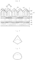
- FIG. 1 is a sectional view showing a solar cell according to the embodiment
- FIGS. 2 to 4 are perspective views showing various examples of an anti-reflective pattern.
- the solar cell includes a support substrate 100, a back electrode layer 200, a light absorbing layer 300, a buffer layer 400, a high resistance buffer layer 500, a window layer 600, and an anti-reflective layer 700.
- the support substrate 100 has a plate shape and supports the back electrode layer 200, the light absorbing layer 300, the buffer layer 400, the high resistance buffer layer 500, and the window layer 600.
- the support substrate 100 may include an insulator.
- the support substrate 100 may include a glass substrate, a plastic substrate, or a metallic substrate.
- the support substrate 100 may include a soda lime glass substrate.
- the support substrate 100 may be transparent or may be rigid or flexible.
- the back electrode layer 200 is provided on the substrate 100.
- the back electrode layer 200 may be a conductive layer.
- the back electrode layer 200 may include a metal, such as molybdenum (Mo).
- the back electrode layer 200 may include at least two layers.
- the layers may be formed by using the homogeneous metal or heterogeneous metals.
- the light absorbing layer 300 is provided on the back electrode layer 200.
- the light absorbing layer 300 includes a group I-III-VI compound.
- the light absorbing layer 300 may have a Cu(In,Ga)Se 2 (CIGS) crystal structure, a Cu(In)Se 2 crystal structure, or a Cu(Ga)Se 2 crystal structure.
- the light absorbing layer 300 may have an energy bandgap in the range of about 1eV to about 1.8eV.
- the buffer layer 400 is provided on the light absorbing layer 300.
- the buffer layer 400 directly makes contact with the light absorbing layer 300.
- the buffer layer 400 may include CdS.
- the buffer layer 400 may have the energy bandgap in the range of about 1.9eV to about 2.3eV.
- the high resistance buffer layer 500 is provided on the buffer layer 400.
- the high-resistance buffer layer 500 may include iZnO, which is zinc oxide not doped with impurities.
- the high resistance buffer layer 500 has an energy bandgap in the range of about 3.1eV to about 3.3eV.
- the window layer 600 is provided on the high resistance buffer layer 500.
- the window layer 600 is transparent, and includes a conductive layer.
- the window layer 600 may include Al doped ZnO (AZO).
- the window layer 600 includes a base layer 610 and an anti-reflective pattern 620.
- the base layer 610 is provided on the high resistance buffer layer 500.
- the anti-reflective pattern 620 protrudes from the base layer 610.
- the anti-reflective pattern 620 is a protrusion pattern.
- the base layer 610 may be integrally formed with the anti-reflective pattern 620.
- the anti-reflective pattern 620 may have various shapes.
- the anti-reflective pattern 620 may have a pyramid shape, a hemispheric shape, or a triangular prim shape.
- the anti-reflective pattern 620 may have a height in the range of about 100nm to about 500nm.
- the height of the anti-reflective pattern 620 may correspond to about 10% to about 50% of the thickness of the window layer 600.
- the anti-reflective pattern 620 includes first inclined surfaces 621 and second inclined surfaces 622.
- the first inclined surfaces 621 are directed to a first direction.
- the first inclined surfaces 621 may extend in the same direction.
- the first inclined surfaces 621 are inclined with respect to a top surface of the support substrate 100.
- the first inclined surfaces 621 are inclined with respect to a top surface of the back electrode layer 200 and a top surface of the light absorbing layer 300.
- An angle between the first inclined surfaces 621 and to top surface of the light absorbing layer 300 may be in the range of about 20° to about 60°.
- an angle between the first inclined surfaces 621 and the top surface of the back electrode layer 200 may be in the range of about 20° to about 60°.
- the second inclined surfaces 622 are directed to a second direction different from the first direction.
- the second inclined surfaces 622 may extend in the same direction.
- the second inclined surfaces 622 may face the first inclined surfaces 621.
- the second inclined surfaces 622 are symmetrical to the first inclined surfaces 621.
- the second inclined surfaces 622 are inclined with respect to the top surface of the support substrate 100. In other words, the second inclined surfaces 622 are inclined with respect to the top surface of the back electrode layer 200 and the top surface of the light absorbing layer 300.
- An angle between the second inclined surfaces 622 and the top surface of the light absorbing layer 300 may be in the range of about 20° to about 60°.
- an angle between the second inclined surfaces 622 and the top surface of the back electrode layer 200 may be in the range of about 20° to about 60°.
- the anti-reflective layer 700 is provided on the window layer 600.
- the anti-reflective layer 700 is coated on the top surface of the window layer 600.
- the anti-reflective layer 700 covers the anti-reflective pattern 620.
- the anti-reflective layer 700 is coated on the surface of the anti-reflective pattern 620.
- the anti-reflective layer 700 is transparent.
- the anti-reflective layer 700 may include anti-reflective coating material such as MgF 2 or LiF.
- the anti-reflective layer 700 includes a fist anti-reflective layer 710 and a second anti-reflective layer 720.
- the first anti-reflective layer 710 is provided on the first inclined surfaces 621.
- the first anti-reflective layer 710 is coated on the first inclined surfaces 621.
- the first anti-reflective layer 710 has a first thickness T1 having a greater size.
- the first thickness T1 of the first anti-reflective layer 710 may be in the range of about 100nm to about 500nm.
- the second anti-reflective layer 720 is provided on the second inclined surfaces 621.
- the second anti-reflective layer 720 is coated on the second inclined surfaces 622.
- the second anti-reflective layer 720 has a second thickness T1 having a smaller size.
- the second thickness T2 of the second anti-reflective layer 720 may be in the range of about 50nm to about 450nm.
- the second thickness T2 is smaller than the first thickness T1.
- the difference between the first thickness T1 and the second thickness T2 may be in the range of about 10nm to about 100nm.
- the first anti-reflective layer 710 is integrally formed with the second anti-reflective layer 720.
- the first anti-reflective layer 710 and the second anti-reflective layer 720 constitute one layer.
- the first anti-reflective layer 710 and the second anti-reflective layer 720 have thicknesses T1 and T2 different from each other, the first anti-reflective layer 710 and the second anti-reflective layer 720 make constructive interference at wavelength bands different from each other.
- an optical path difference between a first light reflected from the first anti-reflective layer 710 and a second light reflected from the first inclined surfaces 621 is twice greater than the first thickness T1.
- the first and second lights make constructive interference at a specific wavelength band due to the optical path difference.
- an optical path difference between a third light reflected from the second anti-reflective layer 720 and a fourth light reflected from the second inclined surfaces 622 is twice greater than the second thickness T2.
- the third and fourth lights make constructive interference at a specific wavelength band due to the optical path difference.
- the first thickness T1 is different from the second thickness T2
- wavelength bands making constructive interference are different from each other. Accordingly, observed colors are different from each other.
- the solar cell according to the embodiment can have an improved external appearance.
- the light incident efficiency of the window layer 600 is improved due to the anti-reflective layer 700 and the anti-reflective pattern 620.
- the solar cell according to the embodiment can represent improved efficiency.
- the embodiment has been described in that the anti-reflective pattern 620 formed in the window layer 600 is coated with the anti-reflective layers 700 having thicknesses different from each other, the embodiment is not limited thereto. Accordingly, the embodiment may have a structure in which anti-reflective layers having different thicknesses are coated on the anti-reflective pattern 620 formed in a protective glass provided on the window layer 600.
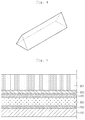
- FIGS. 5 to 8 are sectional views showing the fabricating process of the solar cell according to the embodiment.
- the present fabrication method will be described by making reference to the above description of the solar cell.
- the description of the present fabrication method will be incorporated in the above description of the solar cell.
- the back electrode layer 200 is formed by depositing a metal such as molybdenum (Mo) on the support substrate 100 through a sputtering process.
- the back electrode layer 200 may be formed through two processes having process conditions different from each other.
- An additional layer such as an anti-diffusion layer may be interposed between the support substrate 100 and the back electrode layer 200.
- the light absorbing layer 300 is formed on the back electrode layer 200.
- the light absorbing layer 300 may be formed through a sputtering process or an evaporation scheme.
- the light absorbing layer 300 may be formed through various schemes such as a scheme of forming a Cu(In,Ga)Se2 (CIGS) based light absorbing layer 300 by simultaneously or separately evaporating Cu, In, Ga, and Se and a scheme of performing a selenization process after a metallic precursor layer has been formed.
- CIGS Cu(In,Ga)Se2
- the metallic precursor layer is formed on the back electrode layer 200 through a sputtering process employing a Cu target, an In target, a Ga target or an alloy target.
- the metallic precursor layer is subject to the selenization process so that the Cu (In, Ga) Se2 (CIGS) based light absorbing layer 300 is formed.
- the sputtering process employing the Cu target, the In target, and the Ga target and the selenization process may be simultaneously performed.
- a CIS or a CIG based light absorbing layer 300 may be formed through the sputtering process employing only Cu and In targets or only Cu and Ga targets and the selenization process.
- the buffer layer 400 is formed on the light absorbing layer 300.
- the buffer layer 400 may be formed by depositing CdS on the light absorbing layer 300 through a chemical bath deposition (CBD) process.
- CBD chemical bath deposition
- the high-resistance buffer layer 500 is formed by depositing zinc oxide on the buffer layer 400 through a sputtering process.
- a preliminary window layer 601 is formed on the high resistance buffer layer 500.
- a transparent conductive material is laminated on the high resistance buffer layer 500.
- the transparent conductive material may include AZO.
- a mask pattern 10 is formed on the preliminary window layer 601.
- the mask pattern 10 may be formed through a photolithography process.
- the preliminary window layer 601 is etched by using an etching solution, thereby forming the window layer 600 including the base layer 610 and the anti-reflective pattern 620.
- the etching solution may include a hydrochloric acid solution.
- the top surface of the preliminary window layer 601 may be subject to surface-treatment by using etching particles such as micro sands without employing the mask pattern.
- the anti-reflective layer 700 is formed on the window layer 600.
- a material used to form the anti-reflective layer 700 is deposited on the support substrate 100 while inclining a deposition direction of the material.
- MgF 2 or LiF particles are spread on the window layer 600 from an MgF 2 sputtering target or an LiF sputtering target while inclining a deposition direction of the MgF 2 or LiF particles.
- the spread direction of the above particles may be inclined at an angle of about 20° to about 60° with respect to the top surface of the support substrate 100.
- the materials used to form the anti-reflective layer 700 are spread toward the first inclined surfaces 621.
- the first anti-reflective layer 710 having the first thickness T1 in a greater size is formed on the first inclined surfaces 621, and the second anti-reflective layer 720 having the second thickness T2 in a smaller size is formed on the second inclined surfaces 622.
- a solar cell having an improved external appearance and improved efficiency can be fabricated.
- any reference in this specification to "one embodiment,” “an embodiment,” “example embodiment,” etc. means that a particular feature, structure, or characteristic described in connection with the embodiment is included in at least one embodiment of the invention.
- the appearances of such phrases in various places in the specification are not necessarily all referring to the same embodiment.
Landscapes
- Photovoltaic Devices (AREA)
Claims (10)
- Appareil à cellule solaire comprenant :un substrat (100),une couche d'électrode arrière (200) sur le substrat (100) ;une couche d'absorption de lumière (300) sur la couche d'électrode arrière (200) ;une couche fenêtre (600), sur la couche d'absorption de lumière (300), comportant une couche de base (610) et un motif antireflet (620) faisant saillie de ladite couche de base (610), le motif antireflet (620) comportant une première surface inclinée (621), dirigée vers une première direction, et une seconde surface inclinée (622), dirigée vers une seconde direction, la première surface inclinée (621) et la seconde surface inclinée (622) étant inclinées par rapport à une surface supérieure de la couche d'électrode arrière (200) dans des directions mutuellement différentes ;une couche antireflet (700) fournie sur la couche fenêtre (600) ;dans lequel la couche antireflet (700) a une première couche antireflet (710) et une deuxième couche antireflet (720), la première couche antireflet (710) et la deuxième couche antireflet (720) étant formées d'un seul tenant l'une avec l'autre ;dans lequel des extrémités de la première surface inclinée (621) sont reliées à la seconde surface inclinée (622) et des extrémités de la seconde surface inclinée (622) sont reliées à la première surface inclinée (621) ;dans lequel la première couche antireflet (710) est revêtue sur la première surface inclinée (621) et ayant une première épaisseur uniforme T1 ;dans lequel la deuxième couche antireflet (720) est revêtue sur la seconde surface inclinée (622) et ayant une seconde épaisseur uniforme T2 inférieure à la première épaisseur T1 ;dans lequel la première épaisseur T1 est dans une plage de 100 nm à 500 nm ;dans lequel la seconde épaisseur T2 est dans une plage de 50 nm à 450 nm ; etdans lequel une différence entre les première et seconde épaisseurs T1 et T2 est dans une plage de 10 nm à 100 nm.
- Appareil à cellule solaire selon la revendication 1, dans lequel un angle entre la première surface inclinée (621) et la surface supérieure de la couche d'électrode arrière (200) et un angle entre la seconde surface inclinée (622) et la surface supérieure de la couche d'électrode arrière (200) sont dans une plage de 20° à 60°.
- Appareil à cellule solaire selon la revendication 1, dans lequel les première et deuxième couches antireflets (710, 720) comportent MgF2 ou LiF.
- Appareil à cellule solaire selon la revendication 1, dans lequel le motif antireflet (620) a une forme pyramidale.
- Appareil à cellule solaire selon la revendication 1, comprenant en outre :une troisième couche antireflet sur la première couche antireflet (710) ; etune quatrième couche antireflet sur la deuxième couche antireflet (720),dans lequel la troisième couche antireflet a une épaisseur supérieure à une épaisseur de la quatrième couche antireflet.
- Procédé de fabrication d'un appareil à cellule solaire, le procédé comprenant :la formation d'une couche d'électrode arrière (200) sur un substrat (100) ;la formation d'une couche d'absorption de lumière (300) sur la couche d'électrode arrière (200) ;la formation d'une couche fenêtre (600), sur la couche d'absorption de lumière (300), comportant une couche de base (610) et un motif antireflet (620) faisant saillie de ladite couche de base (610), le motif antireflet (620) comportant une première surface inclinée (621), dirigée vers une première direction, et une seconde surface inclinée (622), dirigée vers une seconde direction, la première surface inclinée (621) et la seconde surface inclinée (622) étant inclinées par rapport à une surface supérieure de la couche d'électrode arrière (200) dans des directions mutuellement différentes ;la formation d'une couche antireflet (700) sur la couche fenêtre (600) ;dans lequel la couche antireflet (700) a une première couche antireflet (710) et une deuxième couche antireflet (720), la première couche antireflet (710) et la deuxième couche antireflet (720) étant formées d'un seul tenant l'une avec l'autre ;dans lequel des extrémités de la première surface inclinée (621) sont reliées à la seconde surface inclinée (622) et des extrémités de la seconde surface inclinée (622) sont reliées à la première surface inclinée (621) ;dans lequel la première couche antireflet (710) est revêtue sur la première surface inclinée (621) et ayant une première épaisseur uniforme T1 ; etdans lequel la deuxième couche antireflet (720) est revêtue sur la seconde surface inclinée (622) et ayant une seconde épaisseur uniforme T2 inférieure à la première épaisseur ;dans lequel la première épaisseur T1 est dans une plage de 100 nm à 500 nm ;dans lequel la seconde épaisseur T1 est dans une plage de 50 nm à 450 nm ; etdans lequel une différence entre les première et seconde épaisseurs T1 et T2 est dans une plage de 10 nm à 100 nm.
- Procédé selon la revendication 6, dans lequel, lors de la formation des première et deuxième couches antireflets (710, 720), les matériaux sources sont déposés dans la direction inclinée par rapport à la surface supérieure de la couche d'électrode arrière (200) selon un angle de 20° à 60°.
- Procédé selon la revendication 7, dans lequel le motif antireflet (620) a une hauteur dans une plage de 100 nm à 500 nm.
- Procédé selon la revendication 6, dans lequel la formation du motif antireflet (620) comprend :la formation d'une couche conductrice transparente sur la couche d'absorption de lumière (300) ; etla gravure d'une partie de la couche conductrice transparente.
- Procédé selon la revendication 6, comprenant en outre :la formation d'une troisième couche antireflet sur la première couche antireflet (710) ; etla formation d'une quatrième couche antireflet sur la deuxième couche antireflet (720),dans lequel la troisième couche antireflet a une épaisseur supérieure à une épaisseur de la quatrième couche antireflet.
Applications Claiming Priority (2)
| Application Number | Priority Date | Filing Date | Title |
|---|---|---|---|
| KR1020100028417A KR101039918B1 (ko) | 2010-03-30 | 2010-03-30 | 태양전지 및 이의 제조방법 |
| PCT/KR2011/002188 WO2011122853A2 (fr) | 2010-03-30 | 2011-03-30 | Dispositif photovoltaïque solaire et son procédé de production |
Publications (3)
| Publication Number | Publication Date |
|---|---|
| EP2560213A2 EP2560213A2 (fr) | 2013-02-20 |
| EP2560213A4 EP2560213A4 (fr) | 2015-11-25 |
| EP2560213B1 true EP2560213B1 (fr) | 2019-10-30 |
Family
ID=44405241
Family Applications (1)
| Application Number | Title | Priority Date | Filing Date |
|---|---|---|---|
| EP11763025.1A Active EP2560213B1 (fr) | 2010-03-30 | 2011-03-30 | Dispositif photovoltaïque solaire et son procédé de production |
Country Status (5)
| Country | Link |
|---|---|
| US (1) | US20130048072A1 (fr) |
| EP (1) | EP2560213B1 (fr) |
| KR (1) | KR101039918B1 (fr) |
| CN (1) | CN102971862B (fr) |
| WO (1) | WO2011122853A2 (fr) |
Families Citing this family (21)
| Publication number | Priority date | Publication date | Assignee | Title |
|---|---|---|---|---|
| KR20120051974A (ko) * | 2010-11-15 | 2012-05-23 | 엘지전자 주식회사 | 태양전지 |
| CN105518876A (zh) * | 2013-07-05 | 2016-04-20 | Gtat公司 | 用于光伏电池的聚硅氮烷涂层 |
| US20150228815A1 (en) * | 2014-02-12 | 2015-08-13 | Tsmc Solar Ltd. | High efficiency solar cells with micro lenses and method for forming the same |
| CN104795454B (zh) * | 2014-12-26 | 2017-05-03 | 天津蓝天太阳科技有限公司 | 砷化镓太阳电池顶电池窗口层纳米圆锥体结构及制备方法 |
| US10937915B2 (en) | 2016-10-28 | 2021-03-02 | Tesla, Inc. | Obscuring, color matching, and camouflaging solar panels |
| US12598838B2 (en) | 2016-11-09 | 2026-04-07 | Tesla, Inc. | System and methods for achieving a micro louver effect in a photovoltaic cell |
| EP3594015A4 (fr) | 2017-03-06 | 2020-07-08 | LG Chem, Ltd. | Élément de décoration et procédé de fabrication d'élément de décoration |
| KR101966851B1 (ko) * | 2017-03-06 | 2019-04-08 | 주식회사 엘지화학 | 장식 부재 및 이의 제조방법 |
| CN108735846A (zh) * | 2017-04-21 | 2018-11-02 | 上银光电股份有限公司 | 具发色图案的薄膜太阳能电池装置 |
| KR101924106B1 (ko) | 2017-06-27 | 2018-11-30 | 주식회사 엘지화학 | 장식 부재 및 이의 제조방법 |
| KR102201549B1 (ko) * | 2017-06-27 | 2021-01-12 | 주식회사 엘지화학 | 장식 부재 및 이의 제조방법 |
| KR101922550B1 (ko) * | 2017-06-27 | 2018-11-27 | 주식회사 엘지화학 | 장식 부재 및 이의 제조방법 |
| US11192334B2 (en) | 2017-06-27 | 2021-12-07 | Lg Chem, Ltd. | Decorative member and method for preparing same |
| KR101925467B1 (ko) | 2017-06-27 | 2018-12-05 | 주식회사 엘지화학 | 장식 부재 및 이의 제조방법 |
| KR101874282B1 (ko) | 2018-01-08 | 2018-07-03 | 주식회사 엘지화학 | 장식 부재 및 이의 제조방법 |
| KR102035907B1 (ko) * | 2017-12-15 | 2019-10-23 | 주식회사 엘지화학 | 장식 부재 및 이의 제조방법 |
| US11971564B2 (en) | 2017-12-15 | 2024-04-30 | Lg Chem, Ltd. | Decorative member and manufacturing method therefor |
| KR102201575B1 (ko) * | 2017-12-15 | 2021-01-12 | 주식회사 엘지화학 | 장식 부재 |
| CN108717949A (zh) * | 2018-06-11 | 2018-10-30 | 汉能移动能源控股集团有限公司 | 一种太阳能电池及其制作方法、太阳能电池组件 |
| CN111564112B (zh) * | 2020-06-09 | 2022-09-23 | 京东方科技集团股份有限公司 | 显示装置、显示面板及其制造方法 |
| KR102338543B1 (ko) * | 2020-12-24 | 2021-12-15 | (주)솔라플렉스 | 발전면적 증가형 태양전지의 제조방법 |
Citations (2)
| Publication number | Priority date | Publication date | Assignee | Title |
|---|---|---|---|---|
| DE19526733A1 (de) * | 1995-07-21 | 1997-01-23 | Siemens Solar Gmbh | Gemusterte Solarzelle |
| CN201051503Y (zh) * | 2006-12-31 | 2008-04-23 | 刘津平 | 单面电极太阳能电池 |
Family Cites Families (17)
| Publication number | Priority date | Publication date | Assignee | Title |
|---|---|---|---|---|
| JPS58121688A (ja) * | 1982-01-14 | 1983-07-20 | Nippon Telegr & Teleph Corp <Ntt> | 太陽電池 |
| KR100408527B1 (ko) | 1996-08-30 | 2004-01-24 | 삼성전자주식회사 | 태양전지및그제조방법 |
| KR19980017427U (ko) * | 1996-09-23 | 1998-07-06 | 양재신 | 차량의 시트에 구비된 암레스트의 접이식 구조 |
| KR100416740B1 (ko) * | 1997-02-17 | 2004-05-17 | 삼성전자주식회사 | 후면 부분소결형 실리콘 태양전지의 제조방법 |
| JP2004363355A (ja) * | 2003-06-05 | 2004-12-24 | Hitachi Ltd | 半導体装置及びその製造方法 |
| CN2733597Y (zh) * | 2004-09-27 | 2005-10-12 | 西安佳阳新能源有限公司 | 彩色光伏组件 |
| US20060130891A1 (en) * | 2004-10-29 | 2006-06-22 | Carlson David E | Back-contact photovoltaic cells |
| US7947893B2 (en) * | 2005-09-30 | 2011-05-24 | Sanyo Electric Co., Ltd. | Solar cell and solar cell module |
| KR100900443B1 (ko) * | 2006-11-20 | 2009-06-01 | 엘지전자 주식회사 | 태양전지 및 그의 제조방법 |
| CN201051502Y (zh) * | 2006-12-31 | 2008-04-23 | 刘津平 | 铜铟镓和硒或硫化物太阳能电池 |
| KR20090017760A (ko) * | 2007-08-16 | 2009-02-19 | 삼성전기주식회사 | 태양전지의 기판 및 그 제조방법 |
| JP4506838B2 (ja) * | 2008-01-17 | 2010-07-21 | 三菱電機株式会社 | 太陽電池及び太陽電池モジュール |
| KR20090098244A (ko) * | 2008-03-13 | 2009-09-17 | 삼성전자주식회사 | 광전소자의 제조 방법 |
| US20110120554A1 (en) * | 2008-03-27 | 2011-05-26 | Rensselaer Polytechnic Institute | Ultra-low reflectance broadband omni-directional anti-reflection coating |
| KR101010286B1 (ko) * | 2008-08-29 | 2011-01-24 | 엘지전자 주식회사 | 태양 전지의 제조 방법 |
| EP2166578A2 (fr) * | 2008-09-22 | 2010-03-24 | Samsung Electronics Co., Ltd. | Dispositif photovoltaïque et son procédé de fabrication |
| KR20110024947A (ko) * | 2009-09-03 | 2011-03-09 | 삼성전자주식회사 | 태양 전지 |
-
2010
- 2010-03-30 KR KR1020100028417A patent/KR101039918B1/ko not_active Expired - Fee Related
-
2011
- 2011-03-30 CN CN201180017045.4A patent/CN102971862B/zh not_active Expired - Fee Related
- 2011-03-30 US US13/638,173 patent/US20130048072A1/en not_active Abandoned
- 2011-03-30 WO PCT/KR2011/002188 patent/WO2011122853A2/fr not_active Ceased
- 2011-03-30 EP EP11763025.1A patent/EP2560213B1/fr active Active
Patent Citations (2)
| Publication number | Priority date | Publication date | Assignee | Title |
|---|---|---|---|---|
| DE19526733A1 (de) * | 1995-07-21 | 1997-01-23 | Siemens Solar Gmbh | Gemusterte Solarzelle |
| CN201051503Y (zh) * | 2006-12-31 | 2008-04-23 | 刘津平 | 单面电极太阳能电池 |
Also Published As
| Publication number | Publication date |
|---|---|
| EP2560213A4 (fr) | 2015-11-25 |
| CN102971862B (zh) | 2015-07-29 |
| WO2011122853A2 (fr) | 2011-10-06 |
| CN102971862A (zh) | 2013-03-13 |
| KR101039918B1 (ko) | 2011-06-09 |
| EP2560213A2 (fr) | 2013-02-20 |
| WO2011122853A3 (fr) | 2012-01-26 |
| US20130048072A1 (en) | 2013-02-28 |
Similar Documents
| Publication | Publication Date | Title |
|---|---|---|
| EP2560213B1 (fr) | Dispositif photovoltaïque solaire et son procédé de production | |
| JP5663030B2 (ja) | 太陽電池及びその製造方法 | |
| US20130037099A1 (en) | Device for generating solar power and method for manufacturing same | |
| US20130025675A1 (en) | Solar cell and method for manufacturing same | |
| CN103988317B (zh) | 太阳能电池及太阳能电池模块 | |
| US9748424B2 (en) | Solar cell and preparing method of the same | |
| KR20090067350A (ko) | 박막형 태양전지 및 그 제조방법 | |
| KR101103894B1 (ko) | 태양전지 및 이의 제조방법 | |
| KR101382898B1 (ko) | 씨스루형 태양전지 모듈 및 이의 제조방법 | |
| JP2013509707A (ja) | 太陽電池及びその製造方法 | |
| US20140238486A1 (en) | Solar cell and method of fabricating the same | |
| US9954122B2 (en) | Solar cell apparatus and method of fabricating the same | |
| US20150027526A1 (en) | Solar cell module and method of fabricating the same | |
| US9966486B2 (en) | Solar cell apparatus and method of fabricating the same | |
| CN103168365A (zh) | 太阳能电池及其制造方法 | |
| US9570636B2 (en) | Solar cell and method of fabricating the same | |
| CN104254926A (zh) | 光伏装置 | |
| EP2432028B1 (fr) | Dispositif photovoltaïque | |
| US20140230896A1 (en) | Solar cell and method of fabricating the same | |
| CN103843148A (zh) | 太阳能电池和使用其的太阳能电池模块 | |
| KR20150056230A (ko) | 패터닝된 그리드전극과 이를 적용한 박막 태양전지 및 이들의 제조방법 | |
| US9660113B2 (en) | Solar cell apparatus and method of fabricating the same | |
| KR101327089B1 (ko) | 태양전지 모듈 및 이의 제조방법 | |
| KR20140047258A (ko) | 태양전지 및 이의 제조 방법 | |
| KR20110050008A (ko) | 태양전지 및 이의 제조방법 |
Legal Events
| Date | Code | Title | Description |
|---|---|---|---|
| PUAI | Public reference made under article 153(3) epc to a published international application that has entered the european phase |
Free format text: ORIGINAL CODE: 0009012 |
|
| 17P | Request for examination filed |
Effective date: 20120711 |
|
| AK | Designated contracting states |
Kind code of ref document: A2 Designated state(s): AL AT BE BG CH CY CZ DE DK EE ES FI FR GB GR HR HU IE IS IT LI LT LU LV MC MK MT NL NO PL PT RO RS SE SI SK SM TR |
|
| DAX | Request for extension of the european patent (deleted) | ||
| A4 | Supplementary search report drawn up and despatched |
Effective date: 20151023 |
|
| RIC1 | Information provided on ipc code assigned before grant |
Ipc: H01L 31/18 20060101ALI20151019BHEP Ipc: H01L 31/046 20140101ALI20151019BHEP Ipc: H01L 31/042 20140101AFI20151019BHEP Ipc: H01L 31/0216 20140101ALI20151019BHEP Ipc: H01L 31/0236 20060101ALI20151019BHEP |
|
| RAP1 | Party data changed (applicant data changed or rights of an application transferred) |
Owner name: LG INNOTEK CO., LTD. |
|
| STAA | Information on the status of an ep patent application or granted ep patent |
Free format text: STATUS: EXAMINATION IS IN PROGRESS |
|
| 17Q | First examination report despatched |
Effective date: 20180612 |
|
| GRAP | Despatch of communication of intention to grant a patent |
Free format text: ORIGINAL CODE: EPIDOSNIGR1 |
|
| STAA | Information on the status of an ep patent application or granted ep patent |
Free format text: STATUS: GRANT OF PATENT IS INTENDED |
|
| INTG | Intention to grant announced |
Effective date: 20190520 |
|
| GRAS | Grant fee paid |
Free format text: ORIGINAL CODE: EPIDOSNIGR3 |
|
| GRAA | (expected) grant |
Free format text: ORIGINAL CODE: 0009210 |
|
| STAA | Information on the status of an ep patent application or granted ep patent |
Free format text: STATUS: THE PATENT HAS BEEN GRANTED |
|
| AK | Designated contracting states |
Kind code of ref document: B1 Designated state(s): AL AT BE BG CH CY CZ DE DK EE ES FI FR GB GR HR HU IE IS IT LI LT LU LV MC MK MT NL NO PL PT RO RS SE SI SK SM TR |
|
| REG | Reference to a national code |
Ref country code: GB Ref legal event code: FG4D |
|
| REG | Reference to a national code |
Ref country code: CH Ref legal event code: EP |
|
| REG | Reference to a national code |
Ref country code: AT Ref legal event code: REF Ref document number: 1197087 Country of ref document: AT Kind code of ref document: T Effective date: 20191115 |
|
| REG | Reference to a national code |
Ref country code: DE Ref legal event code: R096 Ref document number: 602011063060 Country of ref document: DE |
|
| REG | Reference to a national code |
Ref country code: IE Ref legal event code: FG4D |
|
| REG | Reference to a national code |
Ref country code: LT Ref legal event code: MG4D |
|
| PG25 | Lapsed in a contracting state [announced via postgrant information from national office to epo] |
Ref country code: LT Free format text: LAPSE BECAUSE OF FAILURE TO SUBMIT A TRANSLATION OF THE DESCRIPTION OR TO PAY THE FEE WITHIN THE PRESCRIBED TIME-LIMIT Effective date: 20191030 Ref country code: LV Free format text: LAPSE BECAUSE OF FAILURE TO SUBMIT A TRANSLATION OF THE DESCRIPTION OR TO PAY THE FEE WITHIN THE PRESCRIBED TIME-LIMIT Effective date: 20191030 Ref country code: SE Free format text: LAPSE BECAUSE OF FAILURE TO SUBMIT A TRANSLATION OF THE DESCRIPTION OR TO PAY THE FEE WITHIN THE PRESCRIBED TIME-LIMIT Effective date: 20191030 Ref country code: NL Free format text: LAPSE BECAUSE OF FAILURE TO SUBMIT A TRANSLATION OF THE DESCRIPTION OR TO PAY THE FEE WITHIN THE PRESCRIBED TIME-LIMIT Effective date: 20191030 Ref country code: FI Free format text: LAPSE BECAUSE OF FAILURE TO SUBMIT A TRANSLATION OF THE DESCRIPTION OR TO PAY THE FEE WITHIN THE PRESCRIBED TIME-LIMIT Effective date: 20191030 Ref country code: BG Free format text: LAPSE BECAUSE OF FAILURE TO SUBMIT A TRANSLATION OF THE DESCRIPTION OR TO PAY THE FEE WITHIN THE PRESCRIBED TIME-LIMIT Effective date: 20200130 Ref country code: PT Free format text: LAPSE BECAUSE OF FAILURE TO SUBMIT A TRANSLATION OF THE DESCRIPTION OR TO PAY THE FEE WITHIN THE PRESCRIBED TIME-LIMIT Effective date: 20200302 Ref country code: ES Free format text: LAPSE BECAUSE OF FAILURE TO SUBMIT A TRANSLATION OF THE DESCRIPTION OR TO PAY THE FEE WITHIN THE PRESCRIBED TIME-LIMIT Effective date: 20191030 Ref country code: GR Free format text: LAPSE BECAUSE OF FAILURE TO SUBMIT A TRANSLATION OF THE DESCRIPTION OR TO PAY THE FEE WITHIN THE PRESCRIBED TIME-LIMIT Effective date: 20200131 Ref country code: NO Free format text: LAPSE BECAUSE OF FAILURE TO SUBMIT A TRANSLATION OF THE DESCRIPTION OR TO PAY THE FEE WITHIN THE PRESCRIBED TIME-LIMIT Effective date: 20200130 Ref country code: PL Free format text: LAPSE BECAUSE OF FAILURE TO SUBMIT A TRANSLATION OF THE DESCRIPTION OR TO PAY THE FEE WITHIN THE PRESCRIBED TIME-LIMIT Effective date: 20191030 |
|
| REG | Reference to a national code |
Ref country code: NL Ref legal event code: MP Effective date: 20191030 |
|
| PG25 | Lapsed in a contracting state [announced via postgrant information from national office to epo] |
Ref country code: HR Free format text: LAPSE BECAUSE OF FAILURE TO SUBMIT A TRANSLATION OF THE DESCRIPTION OR TO PAY THE FEE WITHIN THE PRESCRIBED TIME-LIMIT Effective date: 20191030 Ref country code: IS Free format text: LAPSE BECAUSE OF FAILURE TO SUBMIT A TRANSLATION OF THE DESCRIPTION OR TO PAY THE FEE WITHIN THE PRESCRIBED TIME-LIMIT Effective date: 20200229 Ref country code: RS Free format text: LAPSE BECAUSE OF FAILURE TO SUBMIT A TRANSLATION OF THE DESCRIPTION OR TO PAY THE FEE WITHIN THE PRESCRIBED TIME-LIMIT Effective date: 20191030 |
|
| PG25 | Lapsed in a contracting state [announced via postgrant information from national office to epo] |
Ref country code: AL Free format text: LAPSE BECAUSE OF FAILURE TO SUBMIT A TRANSLATION OF THE DESCRIPTION OR TO PAY THE FEE WITHIN THE PRESCRIBED TIME-LIMIT Effective date: 20191030 |
|
| PG25 | Lapsed in a contracting state [announced via postgrant information from national office to epo] |
Ref country code: CZ Free format text: LAPSE BECAUSE OF FAILURE TO SUBMIT A TRANSLATION OF THE DESCRIPTION OR TO PAY THE FEE WITHIN THE PRESCRIBED TIME-LIMIT Effective date: 20191030 Ref country code: RO Free format text: LAPSE BECAUSE OF FAILURE TO SUBMIT A TRANSLATION OF THE DESCRIPTION OR TO PAY THE FEE WITHIN THE PRESCRIBED TIME-LIMIT Effective date: 20191030 Ref country code: EE Free format text: LAPSE BECAUSE OF FAILURE TO SUBMIT A TRANSLATION OF THE DESCRIPTION OR TO PAY THE FEE WITHIN THE PRESCRIBED TIME-LIMIT Effective date: 20191030 Ref country code: DK Free format text: LAPSE BECAUSE OF FAILURE TO SUBMIT A TRANSLATION OF THE DESCRIPTION OR TO PAY THE FEE WITHIN THE PRESCRIBED TIME-LIMIT Effective date: 20191030 |
|
| REG | Reference to a national code |
Ref country code: DE Ref legal event code: R097 Ref document number: 602011063060 Country of ref document: DE |
|
| REG | Reference to a national code |
Ref country code: AT Ref legal event code: MK05 Ref document number: 1197087 Country of ref document: AT Kind code of ref document: T Effective date: 20191030 |
|
| PG25 | Lapsed in a contracting state [announced via postgrant information from national office to epo] |
Ref country code: IT Free format text: LAPSE BECAUSE OF FAILURE TO SUBMIT A TRANSLATION OF THE DESCRIPTION OR TO PAY THE FEE WITHIN THE PRESCRIBED TIME-LIMIT Effective date: 20191030 Ref country code: SK Free format text: LAPSE BECAUSE OF FAILURE TO SUBMIT A TRANSLATION OF THE DESCRIPTION OR TO PAY THE FEE WITHIN THE PRESCRIBED TIME-LIMIT Effective date: 20191030 Ref country code: SM Free format text: LAPSE BECAUSE OF FAILURE TO SUBMIT A TRANSLATION OF THE DESCRIPTION OR TO PAY THE FEE WITHIN THE PRESCRIBED TIME-LIMIT Effective date: 20191030 |
|
| PLBE | No opposition filed within time limit |
Free format text: ORIGINAL CODE: 0009261 |
|
| STAA | Information on the status of an ep patent application or granted ep patent |
Free format text: STATUS: NO OPPOSITION FILED WITHIN TIME LIMIT |
|
| 26N | No opposition filed |
Effective date: 20200731 |
|
| PG25 | Lapsed in a contracting state [announced via postgrant information from national office to epo] |
Ref country code: MC Free format text: LAPSE BECAUSE OF FAILURE TO SUBMIT A TRANSLATION OF THE DESCRIPTION OR TO PAY THE FEE WITHIN THE PRESCRIBED TIME-LIMIT Effective date: 20191030 |
|
| REG | Reference to a national code |
Ref country code: CH Ref legal event code: PL |
|
| PG25 | Lapsed in a contracting state [announced via postgrant information from national office to epo] |
Ref country code: SI Free format text: LAPSE BECAUSE OF FAILURE TO SUBMIT A TRANSLATION OF THE DESCRIPTION OR TO PAY THE FEE WITHIN THE PRESCRIBED TIME-LIMIT Effective date: 20191030 Ref country code: AT Free format text: LAPSE BECAUSE OF FAILURE TO SUBMIT A TRANSLATION OF THE DESCRIPTION OR TO PAY THE FEE WITHIN THE PRESCRIBED TIME-LIMIT Effective date: 20191030 |
|
| REG | Reference to a national code |
Ref country code: BE Ref legal event code: MM Effective date: 20200331 |
|
| PG25 | Lapsed in a contracting state [announced via postgrant information from national office to epo] |
Ref country code: LU Free format text: LAPSE BECAUSE OF NON-PAYMENT OF DUE FEES Effective date: 20200330 |
|
| PG25 | Lapsed in a contracting state [announced via postgrant information from national office to epo] |
Ref country code: FR Free format text: LAPSE BECAUSE OF NON-PAYMENT OF DUE FEES Effective date: 20200331 Ref country code: CH Free format text: LAPSE BECAUSE OF NON-PAYMENT OF DUE FEES Effective date: 20200331 Ref country code: LI Free format text: LAPSE BECAUSE OF NON-PAYMENT OF DUE FEES Effective date: 20200331 Ref country code: IE Free format text: LAPSE BECAUSE OF NON-PAYMENT OF DUE FEES Effective date: 20200330 |
|
| PG25 | Lapsed in a contracting state [announced via postgrant information from national office to epo] |
Ref country code: BE Free format text: LAPSE BECAUSE OF NON-PAYMENT OF DUE FEES Effective date: 20200331 |
|
| GBPC | Gb: european patent ceased through non-payment of renewal fee |
Effective date: 20200330 |
|
| PG25 | Lapsed in a contracting state [announced via postgrant information from national office to epo] |
Ref country code: GB Free format text: LAPSE BECAUSE OF NON-PAYMENT OF DUE FEES Effective date: 20200330 |
|
| PG25 | Lapsed in a contracting state [announced via postgrant information from national office to epo] |
Ref country code: TR Free format text: LAPSE BECAUSE OF FAILURE TO SUBMIT A TRANSLATION OF THE DESCRIPTION OR TO PAY THE FEE WITHIN THE PRESCRIBED TIME-LIMIT Effective date: 20191030 Ref country code: MT Free format text: LAPSE BECAUSE OF FAILURE TO SUBMIT A TRANSLATION OF THE DESCRIPTION OR TO PAY THE FEE WITHIN THE PRESCRIBED TIME-LIMIT Effective date: 20191030 Ref country code: CY Free format text: LAPSE BECAUSE OF FAILURE TO SUBMIT A TRANSLATION OF THE DESCRIPTION OR TO PAY THE FEE WITHIN THE PRESCRIBED TIME-LIMIT Effective date: 20191030 |
|
| PG25 | Lapsed in a contracting state [announced via postgrant information from national office to epo] |
Ref country code: MK Free format text: LAPSE BECAUSE OF FAILURE TO SUBMIT A TRANSLATION OF THE DESCRIPTION OR TO PAY THE FEE WITHIN THE PRESCRIBED TIME-LIMIT Effective date: 20191030 |
|
| PGFP | Annual fee paid to national office [announced via postgrant information from national office to epo] |
Ref country code: DE Payment date: 20230220 Year of fee payment: 13 |
|
| REG | Reference to a national code |
Ref country code: DE Ref legal event code: R119 Ref document number: 602011063060 Country of ref document: DE |
|
| PG25 | Lapsed in a contracting state [announced via postgrant information from national office to epo] |
Ref country code: DE Free format text: LAPSE BECAUSE OF NON-PAYMENT OF DUE FEES Effective date: 20241001 |
|
| PG25 | Lapsed in a contracting state [announced via postgrant information from national office to epo] |
Ref country code: DE Free format text: LAPSE BECAUSE OF NON-PAYMENT OF DUE FEES Effective date: 20241001 |