EP2562519A2 - Source de rayonnement - Google Patents
Source de rayonnement Download PDFInfo
- Publication number
- EP2562519A2 EP2562519A2 EP12180539A EP12180539A EP2562519A2 EP 2562519 A2 EP2562519 A2 EP 2562519A2 EP 12180539 A EP12180539 A EP 12180539A EP 12180539 A EP12180539 A EP 12180539A EP 2562519 A2 EP2562519 A2 EP 2562519A2
- Authority
- EP
- European Patent Office
- Prior art keywords
- source
- radiation source
- metallic coating
- radiation
- swelling element
- Prior art date
- Legal status (The legal status is an assumption and is not a legal conclusion. Google has not performed a legal analysis and makes no representation as to the accuracy of the status listed.)
- Granted
Links
Images


Classifications
-
- G—PHYSICS
- G01—MEASURING; TESTING
- G01J—MEASUREMENT OF INTENSITY, VELOCITY, SPECTRAL CONTENT, POLARISATION, PHASE OR PULSE CHARACTERISTICS OF INFRARED, VISIBLE OR ULTRAVIOLET LIGHT; COLORIMETRY; RADIATION PYROMETRY
- G01J3/00—Spectrometry; Spectrophotometry; Monochromators; Measuring colours
- G01J3/02—Details
- G01J3/10—Arrangements of light sources specially adapted for spectrometry or colorimetry
- G01J3/108—Arrangements of light sources specially adapted for spectrometry or colorimetry for measurement in the infrared range
-
- G—PHYSICS
- G01—MEASURING; TESTING
- G01J—MEASUREMENT OF INTENSITY, VELOCITY, SPECTRAL CONTENT, POLARISATION, PHASE OR PULSE CHARACTERISTICS OF INFRARED, VISIBLE OR ULTRAVIOLET LIGHT; COLORIMETRY; RADIATION PYROMETRY
- G01J3/00—Spectrometry; Spectrophotometry; Monochromators; Measuring colours
- G01J3/02—Details
- G01J3/0205—Optical elements not provided otherwise, e.g. optical manifolds, diffusers, windows
- G01J3/0218—Optical elements not provided otherwise, e.g. optical manifolds, diffusers, windows using optical fibers
-
- G—PHYSICS
- G01—MEASURING; TESTING
- G01J—MEASUREMENT OF INTENSITY, VELOCITY, SPECTRAL CONTENT, POLARISATION, PHASE OR PULSE CHARACTERISTICS OF INFRARED, VISIBLE OR ULTRAVIOLET LIGHT; COLORIMETRY; RADIATION PYROMETRY
- G01J3/00—Spectrometry; Spectrophotometry; Monochromators; Measuring colours
- G01J3/28—Investigating the spectrum
- G01J3/42—Absorption spectrometry; Double beam spectrometry; Flicker spectrometry; Reflection spectrometry
-
- H—ELECTRICITY
- H01—ELECTRIC ELEMENTS
- H01K—ELECTRIC INCANDESCENT LAMPS
- H01K1/00—Details
- H01K1/02—Incandescent bodies
- H01K1/04—Incandescent bodies characterised by the material thereof
- H01K1/10—Bodies of metal or carbon combined with other substance
Definitions
- the present invention relates to a radiation source for the emission of infrared electromagnetic radiation, with at least one swelling element.
- the invention relates to an infrared radiation source for use in a gas sensor or gas analyzer or gas spectrometer.
- infrared radiation is radiated into a defined gas volume and the absorption spectrum is recorded.
- Each gas molecule has a characteristic absorption behavior, so that the composition of the gas can be determined from the absorption spectrum.
- infrared spectroscopy is a non-invasive process, it represents a versatile method of chemical analysis. Applications include pharmaceutical analysis, quality control in industrial processes, environmental chemistry, but also geology and astronomy.
- an infrared radiation source is usually a thermal radiator whose surface is heated to correspondingly high temperatures in order to achieve a sufficient radiation intensity in the desired wavelength range.
- a very widespread thermal radiator is a Nernst radiator. Also known is the so-called Globar, a rod made of silicon carbide, which is provided at its ends with electrodes. Electricity is passed through the rod through the electrodes, which heats it up and emits radiation, especially in the infrared range.
- an infrared radiation source consisting essentially of a ceramic rod wrapped with a heating wire, wherein in the ceramic rod a black body cavity is formed, which ultimately emits the infrared radiation.
- An alternative to constantly heated radiation sources are thin-film-based emitters, which are configured as a conductive layer on a substrate. By means of a pulsating heating current applied to the conductive layer, pulsation of the emitted radiation can be achieved.
- a disadvantage of these radiation sources is the high heat loss that occurs due to the direct contact on the substrate.
- an infrared heater for heating a semiconductor wafer which is composed of a flat base, an insulating layer applied thereto, and a heating layer applied to the insulating layer.
- Advantageous materials for the infrared radiation-emitting insulating layer are ceramics such as alumina, zirconia, silicon carbide and diamond.
- incandescent filaments made of a suitable metal or a metal alloy, for example platinum, tungsten, or nickel-chromium.
- a suitable metal or a metal alloy for example platinum, tungsten, or nickel-chromium.
- An example of this group is disclosed in US Pat US 7,122,815 B2 to find. Although they can be operated with pulsating heating current, they nevertheless have a high thermal mass, which entails a high power consumption and moreover requires cooling. Although the thermal mass is reducible by the filament is made correspondingly thin; However, this has the disadvantage that the filament has a low mechanical stability.
- a tungsten wire can only be operated in an oxygen-free atmosphere, which requires its introduction into a housing filled with a protective gas. However, a housing, such as glass, reduces the intensity of the radiation.
- the object of the invention is to provide a modulatable source of infrared radiation which has a low power consumption and a high thermal stability.
- the swelling element is configured as a fiber of silicon carbide, that the swelling element is at least partially coated with a metallic coating over which the swelling element is heated, and that the metallic coating at least temporarily heated the swelling element such that the swelling element at least temporarily emitted infrared radiation.
- the metallic coating serves as a heating element for the silicon carbide fiber so that it can be brought to the temperature required for the emission of infrared radiation.
- the source element is thus not traversed by a heating current itself, but indirectly heated via the coating. By modulating the heat output, the emitted radiation is also modulated.
- the source element emits radiation in the infrared spectral range whenever it has the required temperature due to the heating via the metallic coating. Due to the small diameter of the fiber, the thermal mass of the swelling element is also low, so that a high modulation depth is achieved.
- the at least one silicon carbide fiber is not only mechanically stable, but also has a very good emissivity.
- the fiber of silicon carbide has a diameter below 300 micrometers, preferably below 150 micrometers, in particular between 50 and 150 micrometers.
- the metallic coating consists of platinum or a platinum alloy.
- it is an alloy with iridium, rhodium, zirconium, or a rare earth metal.
- the rare earth metal is preferably yttrium.
- the metallic coating can be direct be applied to the swelling element, or on a previously applied thereto adhesion-promoting intermediate layer, which consists for example of a platinum-chromium or platinum-titanium alloy.
- the metallic coating has a thickness of between 300 and 1800 nanometers.
- the swelling element is applied to a substrate.
- the swelling element is fixed on the substrate, for example, by means of soldering points or high-temperature-resistant glass fixings via the two end regions of the swelling element.
- the fixing points preferably represent the only contact points between the swelling element and the substrate.
- Several swelling elements can also be arranged next to one another on the substrate. This makes it possible to realize a surface radiator.
- the substrate has at least one continuous recess and the swelling element is arranged at least in sections above the recess, so that the swelling element emits radiation at least through the recess.
- a development of the radiation source includes that the swelling element is fastened with its end regions in each case to a holding element and is introduced into a housing.
- no substrate serves as a holder, but two holding elements, for example, rigid wires, which are introduced into a housing.
- the housing is, for example, a metallic transistor housing, preferably a TO transistor housing.
- the support members are made of an electrically conductive material and are configured such that the metallic coating of the swelling element via the support members with an electrical voltage can be acted upon.
- the support elements are designed, for example, as wires to which the swelling element can be fastened by means of solder. The application of voltage to the metallic coating then takes place via the wires connected to the voltage source.
- the metallic coating is applied on one side to the swelling element, so that a section of the swelling element running along a surface line is free of the coating. In the first place then serves the uncoated surface of the radiation of the infrared radiation.
- the swelling element is accordingly applied to the substrate or attached to the support elements such that the coating-free side points in the desired emission direction.
- the metallic coating is applied to the swelling element such that the swelling element is substantially completely encased with the coating.
- the coating thickness can be homogeneous or inhomogeneous.
- the coating is thinner on the side which faces in the direction of radiation than on the opposite side.
- the layer thickness is substantially constant along a surface line.
- the object underlying the invention is achieved by a method for producing a radiation source wherein at least one fiber of silicon carbide is applied to at least two attachment points on a substrate, wherein the fiber and at least two portions of the substrate in which the attachment points lie, with a metallic coating are coated, and wherein the two portions of the substrate, which are coated with the metallic coating, are contacted with electrical leads, so that an electrical voltage to the metallic coating of the fiber can be applied.
- the swelling element ie the silicon carbide fiber
- the swelling element is coated on one side. If the uncoated swelling element is attached to the substrate, its rear side remote from the substrate can be coated particularly easily.
- the contacting of the swelling element can take place directly over the substrate, provided that the coating has at least one interruption on the substrate, which electrically separates the substrate sections which are in contact with the two end regions of the swelling element.
- the invention comprises a gas sensor for analyzing a gas mixture and / or detecting one or more gases, which has at least one radiation source according to one or more of the preceding embodiments.
- a gas can be examined for its composition or a specific gas can be detected.
- the gas sensor is configured to detect or quantitatively detect at least one of the gases carbon dioxide, ethanol, ammonia and methane.
- the gas sensor can also be used for other gases. Gas sensors with radiation sources for the emission of infrared radiation are known from the prior art, so that it is not discussed in more detail here on their operation.
- the radiation source according to the invention with one or more silicon carbide fibers as swelling element offers a number of advantages.
- the source element has a high emissivity over a wide wavelength range in the infrared spectrum.
- the radiation emission is electrically modulated via the metal coating designed as a resistance heating. This eliminates mechanical modulators, resulting in a more compact and less expensive construction of the radiation source.
- the swelling element Due to the low thermal mass, the swelling element has a fast response time, allowing fast modulation at high modulation depth.
- the power consumption is low and the efficiency is high, which makes the radiation source cost and energy efficient. Cooling of the swelling element is also unnecessary due to the low power consumption.
- the radiation source has a long life even at high temperatures and a long-term stable emission spectrum. In contrast to a tungsten wire, a SiC fiber can be operated in any oxygen-containing environment.
- the coated swelling element can be applied in a large variety of variants on carriers or brackets and placed in various types of housing, so that a suitable design is possible for each application. Since silicon carbide is stable under normal atmosphere, introduction into an evacuated or protective gas-filled sleeve is not required. For certain However, in applications where a particular ambient gas is advantageous, for example, for filtering certain wavelengths, encapsulation is possible.
- Fig. 1 a is the structure of a coated swelling element 21 shown schematically on the basis of a section along a longitudinal axis of the swelling element 2-containing plane.
- the infrared radiation emitting source element 2 is a fiber of silicon carbide.
- a fiber here is to be understood as meaning a very thin element whose length exceeds the diameter by several orders of magnitude.
- the diameter of the swelling element 2 is as small as possible and is for example between 50 and 300 micrometers, preferably between 50 and 150 micrometers.
- the swelling element 2 has two coatings 3, 4, wherein the outer coating is a metallic coating 3, which acts as a heating element and is therefore characterized by a high electrical resistance.
- the intermediate layer 4 arranged below the metallic coating 3 is an adhesion-promoting layer which leads to improved adhesion of the metallic coating 3 on the silicon carbide fiber.
- the intermediate layer 4 can also be omitted.
- the metallic coating 3 is preferably made of platinum or a platinum alloy, for example of platinum-iridium, platinum-rhodium, or platinum-zirconium. Also suitable are alloys of platinum and a rare earth metal, in particular yttrium. The alloys mentioned have high stability even at high temperatures.
- the fat The metallic coating 3 is for example 800 nm. In general, its thickness is preferably between 300 and 2000 nanometers, particularly preferably 500 to 900 nanometers.
- the adhesion-promoting intermediate layer 4 also contains platinum in accordance with the metallic coating 3.
- it is a platinum-chromium or platinum-titanium alloy. In principle, however, any materials with adhesion-promoting effect can be used.
- the layer thickness of the intermediate layer 4 is preferably about 40-150 nanometers, in particular about 40 nanometers.
- the metallic coating 3, as well as the intermediate layer 4, are in the in Fig. 1 a embodiment shown only one side applied to the swelling element 2.
- the coatings 3, 4 can also completely surround the swelling element 2, wherein the thickness of the coatings 3, 4 can each be homogeneous or varied.
- Fig. 1c and 1d shown show a sectional view of the coated swelling element 21 in a perpendicular to the longitudinal axis of the swelling element 2 extending plane AA.
- Fig. 1b shows a corresponding sectional view of in Fig. 1 a shown embodiment.
- Fig. 1c illustrates the case that the coating 3 is applied on one side, so that a portion of the swelling element 2, which runs along a surface line, is free of the coating 3.
- approximately one half of the lateral surface of the swelling element 2 is provided with a very thin metallic coating 3, while the other half has a thicker coating 3.
- the thin part of the coating 3 then serves primarily as protection of the swelling element 2 against corrosion or damage to the surface, while the thick part of the coating 3 mainly assumes the function of heating the swelling element 2.
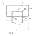
- Fig. 2 discloses an embodiment of a radiation source 1 for a gas sensor in which the coated swelling element 21 is mounted in a transistor housing.
- the transistor package is a common metallic TO package.
- the use of such housing for infrared radiation sources with a tungsten wire is known for example from the US patent US 7122815 B2 known.
- the connecting pins 5 extend through a base plate 61 into a circular-cylindrical metallic head part 6.
- the bushings are in this case sealed with glass or another insulating material 62 and electrically insulated from the base plate 61.
- the transistor housing is closed with a transmission window 7, through which the radiation emitted by the source element 2 emerges, while the transistor housing itself is opaque to the radiation.
- the material of the transmission window 7 is tuned to the wavelengths of the emitted radiation.
- sapphire, CaF 2 , BaF 2 , ZnSe or silicon coated with an anti-reflection layer are suitable for the transmission of infrared radiation.
- connection pins 5 and the end regions of the coated source element 21 are connected to one another via soldering points 51.
- an electrically conductive connection between the connecting pins 5 and the metallic coating 3 of the swelling element 2 is created.
- a voltage source connected to the connection pins 5 a voltage can be applied to the metallic coating 3.
- the latter heats up according to the applied voltage or the heating power to a certain temperature, whereby the source element 2 is heated accordingly.
- the temperature of the source element 2 is adjusted so that it emits primarily electromagnetic radiation in a predetermined wavelength range. For use in a gas spectrometer, this is infrared radiation, in particular near and mid-infrared radiation having wavelengths preferably between 1 and 5 micrometers and between 7 and 20 micrometers.
- the source element 2 may also emit pulsed radiation when the heating power or the amplitude of the applied voltage pulses.
- the applied voltage may in this case be an AC voltage or else an AC voltage with DC voltage component.
- the waveform of the voltage is arbitrary and may be symmetrical or asymmetrical shape. For example, a square, triangular, or sawtooth voltage, or a sinusoidal voltage is applied. Also a variation of the frequency for power control is possible.
- the source element 2 Due to the configuration of the source element 2 as a fiber, it has a very low thermal mass, so that the swelling element 2 reacts quickly to a change in the heating temperature and the radiated infrared radiation has a high modulation depth even at relatively high frequencies.
- relatively high already means more than a few hertz, for example 10-20 Hz.
- modulation with higher frequencies for example 50 Hz or more, is also possible.
- a modulation of the emitted radiation enables the suppression of interference signals when using the radiation source 1 in an infrared spectrometer.
- By modulating the applied voltage eliminates means for mechanical modulation of the radiation, such as pinhole, which makes this structure of a radiation source 1 compact and inexpensive.
- Fig. 3a-d show by way of example various embodiments of a substrate 8 with one or more applied source elements 2 in a schematic plan view.
- the substrate 8 is, for example, an aluminum oxide or zirconium oxide substrate 8.
- a swelling element 2 is applied to a square substrate 8.
- the swelling element 2 is arranged such that it lies in sections over a recess 81 in the substrate 8.
- a plurality of recesses of the same or different shape and size can be introduced into the substrate 8. These can be designed as a notch or centrally in the substrate 8 as shown.
- the installation of the radiation source 1 in a sensor therefore takes place in a corresponding manner such that the side of the substrate on which the swelling element 2 is located faces away from the object to be irradiated.
- the connection between the source element 2 and the substrate 8 is, for example produced via splices or by means of glass fixations, the fixations are high temperature resistant.
- the substrate 8 is provided with an electrically conductive coating, at least in two sections, which are in each case in contact with a contact point to the coated swelling element 21.
- the two sections can be designed as tracks or flat; The important thing is that they are electrically isolated from each other.
- the coating of the substrate 8 is preferably the same metallic coating 3 with which the swelling element 2 is also coated. This is particularly effective if the swelling element 2 is only coated on one side, since substrate 8 and swelling element 2 can then be coated in a common process step.
- an electrical supply line 9 is attached, for example at a soldering point or on a contact pad. Connected to the electrical leads 9 is the voltage source for supplying the metallic coating 3 of the source element 2 with a heating current.
- Fig. 3b shows a substantially same structure as Fig. 3a , Instead of a single source element 2, two source elements 2 are arranged above the recess 81 in the substrate 8 in order to increase the radiation intensity.
- the number of source elements 2 is not limited to one or two.
- the substrate 8 can serve as carrier for any number of swelling elements 2. By arranging a plurality of swelling elements 2 next to one another, preferably parallel to one another, an areal radiation characteristic can be achieved.
- Fig. 3c an alternative embodiment is shown with a rectangular substrate 8, which has an oval, centrally introduced into the substrate 8 recess 81.
- the swelling element 2 is arranged above the recess 81.
- the end portions of the swelling member 2 terminate on the substrate 8 where they are fixed.
- the fixation is preferably limited to a small area, instead of flat.
- the fixation consists of a glass gob.
- the contacting takes place as in Fig. 3a or 3b over the substrate 8.
- the electrical leads 9 are directly connected to the End portions of the source element 2 connected. This contacting variant is the same for the embodiments according to Fig. 3a or 3b possible.
- Fig. 3d shows one to the embodiment Fig. 3c similar embodiment, wherein three coated swelling elements 21 are arranged parallel to each other above the recess 81 in the substrate 8. Since the coated source elements 21 are preferably all connected to the same voltage source, contacting via a coating of the substrate 8 is advantageous. There are then only two electrical contact lines required.
Landscapes
- Physics & Mathematics (AREA)
- Spectroscopy & Molecular Physics (AREA)
- General Physics & Mathematics (AREA)
- Investigating Or Analysing Materials By Optical Means (AREA)
- Resistance Heating (AREA)
- Ceramic Products (AREA)
Applications Claiming Priority (1)
| Application Number | Priority Date | Filing Date | Title |
|---|---|---|---|
| DE102011081570.8A DE102011081570B4 (de) | 2011-08-25 | 2011-08-25 | Strahlungsquelle |
Publications (3)
| Publication Number | Publication Date |
|---|---|
| EP2562519A2 true EP2562519A2 (fr) | 2013-02-27 |
| EP2562519A3 EP2562519A3 (fr) | 2017-12-20 |
| EP2562519B1 EP2562519B1 (fr) | 2020-02-19 |
Family
ID=46799047
Family Applications (1)
| Application Number | Title | Priority Date | Filing Date |
|---|---|---|---|
| EP12180539.4A Active EP2562519B1 (fr) | 2011-08-25 | 2012-08-15 | Source de rayonnement |
Country Status (3)
| Country | Link |
|---|---|
| US (1) | US8610067B2 (fr) |
| EP (1) | EP2562519B1 (fr) |
| DE (1) | DE102011081570B4 (fr) |
Citations (3)
| Publication number | Priority date | Publication date | Assignee | Title |
|---|---|---|---|---|
| EP0106431B1 (fr) | 1982-10-18 | 1987-10-07 | Hewlett-Packard Company | Elément de source rayonnante infrarouge |
| JPH0325880A (ja) | 1989-06-23 | 1991-02-04 | Tokyo Erekutoron Kyushu Kk | 加熱方法及び加熱装置 |
| US7122815B2 (en) | 2003-05-27 | 2006-10-17 | Wood Donald S | Infrared radiation emitter |
Family Cites Families (8)
| Publication number | Priority date | Publication date | Assignee | Title |
|---|---|---|---|---|
| US3100828A (en) | 1959-09-08 | 1963-08-13 | Jacobs Gerhard | Source of radiation for infrared spectrophotometers |
| JPS6041136B2 (ja) * | 1976-09-01 | 1985-09-14 | 財団法人特殊無機材料研究所 | シリコンカ−バイド繊維強化軽金属複合材料の製造方法 |
| JPS61240033A (ja) | 1985-04-16 | 1986-10-25 | Matsushita Electric Ind Co Ltd | 調理器 |
| DE68913533T2 (de) | 1989-09-29 | 1994-10-13 | Nippon Carbon Co Ltd | Infrarot-Detektor-Element. |
| DE69215766D1 (de) * | 1991-06-17 | 1997-01-23 | Gen Electric | Siliziumcarbid-Verbundwerkstoff verstärkt mit Metallnitrid beschichteten Fasern |
| US5616650A (en) * | 1993-11-05 | 1997-04-01 | Lanxide Technology Company, Lp | Metal-nitrogen polymer compositions comprising organic electrophiles |
| FR2748810A1 (fr) | 1996-09-30 | 1997-11-21 | Commissariat Energie Atomique | Source de rayonnement infrarouge miniaturisee |
| AU2001255308A1 (en) * | 2000-04-26 | 2001-11-07 | Cornell Research Foundation Inc. | Lamp utilizing fiber for enhanced starting field |
-
2011
- 2011-08-25 DE DE102011081570.8A patent/DE102011081570B4/de active Active
-
2012
- 2012-08-15 EP EP12180539.4A patent/EP2562519B1/fr active Active
- 2012-08-23 US US13/592,549 patent/US8610067B2/en active Active
Patent Citations (3)
| Publication number | Priority date | Publication date | Assignee | Title |
|---|---|---|---|---|
| EP0106431B1 (fr) | 1982-10-18 | 1987-10-07 | Hewlett-Packard Company | Elément de source rayonnante infrarouge |
| JPH0325880A (ja) | 1989-06-23 | 1991-02-04 | Tokyo Erekutoron Kyushu Kk | 加熱方法及び加熱装置 |
| US7122815B2 (en) | 2003-05-27 | 2006-10-17 | Wood Donald S | Infrared radiation emitter |
Also Published As
| Publication number | Publication date |
|---|---|
| DE102011081570B4 (de) | 2023-08-17 |
| EP2562519A3 (fr) | 2017-12-20 |
| US8610067B2 (en) | 2013-12-17 |
| DE102011081570A1 (de) | 2013-02-28 |
| US20130057850A1 (en) | 2013-03-07 |
| EP2562519B1 (fr) | 2020-02-19 |
Similar Documents
| Publication | Publication Date | Title |
|---|---|---|
| DE69512141T2 (de) | Elektrisch modulierbare thermische Strahlungsquelle | |
| EP3155871B1 (fr) | Element chauffant plan avec une structure resistante ptc | |
| DE3019387A1 (de) | Duennschicht-halbleiter-gassensor mit einem in den sensor integrierten heizelement | |
| DE19750123C2 (de) | Verfahren zur Herstellung einer Sensoranordnung für die Temperaturmessung | |
| DE3437397A1 (de) | Infrarot-strahler | |
| DE102014103429A1 (de) | Sensor und Sensorikverfahren | |
| EP2406607B1 (fr) | Dispositif de rayonnement infrarouge pour analyseur de gaz | |
| DE19753642C2 (de) | Verfahren zur Herstellung eines elektrischen Widerstands | |
| EP0168589A1 (fr) | Détecteur d'oxygène | |
| DE4419285C2 (de) | Infrarotstrahler | |
| DE2933971C2 (de) | Gassensor hoher Empfindlichkeit und Stabilität zum Nachweis und zur Messung des Verunreinigungsgehaltes von Luft auf der Basis von Metalloxidhalbleitern | |
| DE19611964A1 (de) | Gasmeßfühler | |
| WO2009024291A1 (fr) | Module laser accordable spectralement | |
| EP2562519B1 (fr) | Source de rayonnement | |
| DE10020931C1 (de) | Temperaturmessfühler und Verfahren zur Kontaktierung eines Temperaturmessfühlers | |
| DE2710861B2 (de) | Verfahren zur Atomisierung von in einem Atomabsorptionsspektrometer zu untersuchenden Proben und Vorrichtung zur Durchführung dieses Verfahrens | |
| DE102004046123A1 (de) | Kohärente Terahertz-Strahlungsquelle | |
| DE3139617A1 (de) | Gassensor und verfahren zu seiner hertellung | |
| DE4334410A1 (de) | Dünnschicht-Gassensor | |
| EP2929311B1 (fr) | Thermocouple | |
| DE4134998A1 (de) | Vakuumfluoreszenzanzeigeroehre | |
| DE19734650B4 (de) | Vorrichtung zur Emission elektromagnetischer Strahlung durch Gasentladung, Verfahren zu ihrer Herstellung und Verwendung der Vorrichtung | |
| DE102005014106B4 (de) | Temperatursensor und Verfahren zur Herstellung | |
| DE1943748A1 (de) | Heiz- und Temperaturmessgeraet | |
| DE102017128664A1 (de) | Strahlungsquelle zur Erzeugung einer elektromagnetischen Strahlung sowie Verfahren zu ihrer Herstellung |
Legal Events
| Date | Code | Title | Description |
|---|---|---|---|
| PUAI | Public reference made under article 153(3) epc to a published international application that has entered the european phase |
Free format text: ORIGINAL CODE: 0009012 |
|
| AK | Designated contracting states |
Kind code of ref document: A2 Designated state(s): AL AT BE BG CH CY CZ DE DK EE ES FI FR GB GR HR HU IE IS IT LI LT LU LV MC MK MT NL NO PL PT RO RS SE SI SK SM TR |
|
| AX | Request for extension of the european patent |
Extension state: BA ME |
|
| RAP1 | Party data changed (applicant data changed or rights of an application transferred) |
Owner name: INNOVATIVE SENSOR TECHNOLOGY IST AG |
|
| REG | Reference to a national code |
Ref country code: DE Ref legal event code: R079 Ref document number: 502012015778 Country of ref document: DE Free format text: PREVIOUS MAIN CLASS: G01J0003100000 Ipc: H01K0001100000 |
|
| PUAL | Search report despatched |
Free format text: ORIGINAL CODE: 0009013 |
|
| AK | Designated contracting states |
Kind code of ref document: A3 Designated state(s): AL AT BE BG CH CY CZ DE DK EE ES FI FR GB GR HR HU IE IS IT LI LT LU LV MC MK MT NL NO PL PT RO RS SE SI SK SM TR |
|
| AX | Request for extension of the european patent |
Extension state: BA ME |
|
| RIC1 | Information provided on ipc code assigned before grant |
Ipc: G01J 3/42 20060101ALI20171113BHEP Ipc: H01K 1/10 20060101AFI20171113BHEP Ipc: G01J 3/10 20060101ALI20171113BHEP Ipc: G01J 3/02 20060101ALI20171113BHEP |
|
| STAA | Information on the status of an ep patent application or granted ep patent |
Free format text: STATUS: REQUEST FOR EXAMINATION WAS MADE |
|
| 17P | Request for examination filed |
Effective date: 20180111 |
|
| RBV | Designated contracting states (corrected) |
Designated state(s): AL AT BE BG CH CY CZ DE DK EE ES FI FR GB GR HR HU IE IS IT LI LT LU LV MC MK MT NL NO PL PT RO RS SE SI SK SM TR |
|
| STAA | Information on the status of an ep patent application or granted ep patent |
Free format text: STATUS: EXAMINATION IS IN PROGRESS |
|
| 17Q | First examination report despatched |
Effective date: 20181004 |
|
| GRAP | Despatch of communication of intention to grant a patent |
Free format text: ORIGINAL CODE: EPIDOSNIGR1 |
|
| STAA | Information on the status of an ep patent application or granted ep patent |
Free format text: STATUS: GRANT OF PATENT IS INTENDED |
|
| INTG | Intention to grant announced |
Effective date: 20191007 |
|
| GRAS | Grant fee paid |
Free format text: ORIGINAL CODE: EPIDOSNIGR3 |
|
| GRAA | (expected) grant |
Free format text: ORIGINAL CODE: 0009210 |
|
| STAA | Information on the status of an ep patent application or granted ep patent |
Free format text: STATUS: THE PATENT HAS BEEN GRANTED |
|
| AK | Designated contracting states |
Kind code of ref document: B1 Designated state(s): AL AT BE BG CH CY CZ DE DK EE ES FI FR GB GR HR HU IE IS IT LI LT LU LV MC MK MT NL NO PL PT RO RS SE SI SK SM TR |
|
| REG | Reference to a national code |
Ref country code: GB Ref legal event code: FG4D Free format text: NOT ENGLISH |
|
| REG | Reference to a national code |
Ref country code: CH Ref legal event code: EP |
|
| REG | Reference to a national code |
Ref country code: DE Ref legal event code: R096 Ref document number: 502012015778 Country of ref document: DE |
|
| REG | Reference to a national code |
Ref country code: AT Ref legal event code: REF Ref document number: 1235917 Country of ref document: AT Kind code of ref document: T Effective date: 20200315 |
|
| REG | Reference to a national code |
Ref country code: IE Ref legal event code: FG4D Free format text: LANGUAGE OF EP DOCUMENT: GERMAN |
|
| REG | Reference to a national code |
Ref country code: NL Ref legal event code: MP Effective date: 20200219 |
|
| PG25 | Lapsed in a contracting state [announced via postgrant information from national office to epo] |
Ref country code: RS Free format text: LAPSE BECAUSE OF FAILURE TO SUBMIT A TRANSLATION OF THE DESCRIPTION OR TO PAY THE FEE WITHIN THE PRESCRIBED TIME-LIMIT Effective date: 20200219 Ref country code: FI Free format text: LAPSE BECAUSE OF FAILURE TO SUBMIT A TRANSLATION OF THE DESCRIPTION OR TO PAY THE FEE WITHIN THE PRESCRIBED TIME-LIMIT Effective date: 20200219 Ref country code: NO Free format text: LAPSE BECAUSE OF FAILURE TO SUBMIT A TRANSLATION OF THE DESCRIPTION OR TO PAY THE FEE WITHIN THE PRESCRIBED TIME-LIMIT Effective date: 20200519 |
|
| REG | Reference to a national code |
Ref country code: LT Ref legal event code: MG4D |
|
| PG25 | Lapsed in a contracting state [announced via postgrant information from national office to epo] |
Ref country code: HR Free format text: LAPSE BECAUSE OF FAILURE TO SUBMIT A TRANSLATION OF THE DESCRIPTION OR TO PAY THE FEE WITHIN THE PRESCRIBED TIME-LIMIT Effective date: 20200219 Ref country code: LV Free format text: LAPSE BECAUSE OF FAILURE TO SUBMIT A TRANSLATION OF THE DESCRIPTION OR TO PAY THE FEE WITHIN THE PRESCRIBED TIME-LIMIT Effective date: 20200219 Ref country code: SE Free format text: LAPSE BECAUSE OF FAILURE TO SUBMIT A TRANSLATION OF THE DESCRIPTION OR TO PAY THE FEE WITHIN THE PRESCRIBED TIME-LIMIT Effective date: 20200219 Ref country code: IS Free format text: LAPSE BECAUSE OF FAILURE TO SUBMIT A TRANSLATION OF THE DESCRIPTION OR TO PAY THE FEE WITHIN THE PRESCRIBED TIME-LIMIT Effective date: 20200619 Ref country code: BG Free format text: LAPSE BECAUSE OF FAILURE TO SUBMIT A TRANSLATION OF THE DESCRIPTION OR TO PAY THE FEE WITHIN THE PRESCRIBED TIME-LIMIT Effective date: 20200519 Ref country code: GR Free format text: LAPSE BECAUSE OF FAILURE TO SUBMIT A TRANSLATION OF THE DESCRIPTION OR TO PAY THE FEE WITHIN THE PRESCRIBED TIME-LIMIT Effective date: 20200520 |
|
| PG25 | Lapsed in a contracting state [announced via postgrant information from national office to epo] |
Ref country code: NL Free format text: LAPSE BECAUSE OF FAILURE TO SUBMIT A TRANSLATION OF THE DESCRIPTION OR TO PAY THE FEE WITHIN THE PRESCRIBED TIME-LIMIT Effective date: 20200219 |
|
| PG25 | Lapsed in a contracting state [announced via postgrant information from national office to epo] |
Ref country code: RO Free format text: LAPSE BECAUSE OF FAILURE TO SUBMIT A TRANSLATION OF THE DESCRIPTION OR TO PAY THE FEE WITHIN THE PRESCRIBED TIME-LIMIT Effective date: 20200219 Ref country code: SK Free format text: LAPSE BECAUSE OF FAILURE TO SUBMIT A TRANSLATION OF THE DESCRIPTION OR TO PAY THE FEE WITHIN THE PRESCRIBED TIME-LIMIT Effective date: 20200219 Ref country code: PT Free format text: LAPSE BECAUSE OF FAILURE TO SUBMIT A TRANSLATION OF THE DESCRIPTION OR TO PAY THE FEE WITHIN THE PRESCRIBED TIME-LIMIT Effective date: 20200712 Ref country code: CZ Free format text: LAPSE BECAUSE OF FAILURE TO SUBMIT A TRANSLATION OF THE DESCRIPTION OR TO PAY THE FEE WITHIN THE PRESCRIBED TIME-LIMIT Effective date: 20200219 Ref country code: DK Free format text: LAPSE BECAUSE OF FAILURE TO SUBMIT A TRANSLATION OF THE DESCRIPTION OR TO PAY THE FEE WITHIN THE PRESCRIBED TIME-LIMIT Effective date: 20200219 Ref country code: ES Free format text: LAPSE BECAUSE OF FAILURE TO SUBMIT A TRANSLATION OF THE DESCRIPTION OR TO PAY THE FEE WITHIN THE PRESCRIBED TIME-LIMIT Effective date: 20200219 Ref country code: LT Free format text: LAPSE BECAUSE OF FAILURE TO SUBMIT A TRANSLATION OF THE DESCRIPTION OR TO PAY THE FEE WITHIN THE PRESCRIBED TIME-LIMIT Effective date: 20200219 Ref country code: SM Free format text: LAPSE BECAUSE OF FAILURE TO SUBMIT A TRANSLATION OF THE DESCRIPTION OR TO PAY THE FEE WITHIN THE PRESCRIBED TIME-LIMIT Effective date: 20200219 Ref country code: EE Free format text: LAPSE BECAUSE OF FAILURE TO SUBMIT A TRANSLATION OF THE DESCRIPTION OR TO PAY THE FEE WITHIN THE PRESCRIBED TIME-LIMIT Effective date: 20200219 |
|
| REG | Reference to a national code |
Ref country code: DE Ref legal event code: R097 Ref document number: 502012015778 Country of ref document: DE |
|
| PLBE | No opposition filed within time limit |
Free format text: ORIGINAL CODE: 0009261 |
|
| STAA | Information on the status of an ep patent application or granted ep patent |
Free format text: STATUS: NO OPPOSITION FILED WITHIN TIME LIMIT |
|
| 26N | No opposition filed |
Effective date: 20201120 |
|
| PG25 | Lapsed in a contracting state [announced via postgrant information from national office to epo] |
Ref country code: IT Free format text: LAPSE BECAUSE OF FAILURE TO SUBMIT A TRANSLATION OF THE DESCRIPTION OR TO PAY THE FEE WITHIN THE PRESCRIBED TIME-LIMIT Effective date: 20200219 |
|
| PG25 | Lapsed in a contracting state [announced via postgrant information from national office to epo] |
Ref country code: SI Free format text: LAPSE BECAUSE OF FAILURE TO SUBMIT A TRANSLATION OF THE DESCRIPTION OR TO PAY THE FEE WITHIN THE PRESCRIBED TIME-LIMIT Effective date: 20200219 Ref country code: PL Free format text: LAPSE BECAUSE OF FAILURE TO SUBMIT A TRANSLATION OF THE DESCRIPTION OR TO PAY THE FEE WITHIN THE PRESCRIBED TIME-LIMIT Effective date: 20200219 |
|
| PG25 | Lapsed in a contracting state [announced via postgrant information from national office to epo] |
Ref country code: MC Free format text: LAPSE BECAUSE OF FAILURE TO SUBMIT A TRANSLATION OF THE DESCRIPTION OR TO PAY THE FEE WITHIN THE PRESCRIBED TIME-LIMIT Effective date: 20200219 |
|
| PG25 | Lapsed in a contracting state [announced via postgrant information from national office to epo] |
Ref country code: LU Free format text: LAPSE BECAUSE OF NON-PAYMENT OF DUE FEES Effective date: 20200815 |
|
| REG | Reference to a national code |
Ref country code: BE Ref legal event code: MM Effective date: 20200831 |
|
| PG25 | Lapsed in a contracting state [announced via postgrant information from national office to epo] |
Ref country code: IE Free format text: LAPSE BECAUSE OF NON-PAYMENT OF DUE FEES Effective date: 20200815 Ref country code: BE Free format text: LAPSE BECAUSE OF NON-PAYMENT OF DUE FEES Effective date: 20200831 |
|
| REG | Reference to a national code |
Ref country code: AT Ref legal event code: MM01 Ref document number: 1235917 Country of ref document: AT Kind code of ref document: T Effective date: 20200815 |
|
| PG25 | Lapsed in a contracting state [announced via postgrant information from national office to epo] |
Ref country code: AT Free format text: LAPSE BECAUSE OF NON-PAYMENT OF DUE FEES Effective date: 20200815 |
|
| PG25 | Lapsed in a contracting state [announced via postgrant information from national office to epo] |
Ref country code: TR Free format text: LAPSE BECAUSE OF FAILURE TO SUBMIT A TRANSLATION OF THE DESCRIPTION OR TO PAY THE FEE WITHIN THE PRESCRIBED TIME-LIMIT Effective date: 20200219 Ref country code: MT Free format text: LAPSE BECAUSE OF FAILURE TO SUBMIT A TRANSLATION OF THE DESCRIPTION OR TO PAY THE FEE WITHIN THE PRESCRIBED TIME-LIMIT Effective date: 20200219 Ref country code: CY Free format text: LAPSE BECAUSE OF FAILURE TO SUBMIT A TRANSLATION OF THE DESCRIPTION OR TO PAY THE FEE WITHIN THE PRESCRIBED TIME-LIMIT Effective date: 20200219 |
|
| PG25 | Lapsed in a contracting state [announced via postgrant information from national office to epo] |
Ref country code: MK Free format text: LAPSE BECAUSE OF FAILURE TO SUBMIT A TRANSLATION OF THE DESCRIPTION OR TO PAY THE FEE WITHIN THE PRESCRIBED TIME-LIMIT Effective date: 20200219 Ref country code: AL Free format text: LAPSE BECAUSE OF FAILURE TO SUBMIT A TRANSLATION OF THE DESCRIPTION OR TO PAY THE FEE WITHIN THE PRESCRIBED TIME-LIMIT Effective date: 20200219 |
|
| P01 | Opt-out of the competence of the unified patent court (upc) registered |
Effective date: 20230601 |
|
| PGFP | Annual fee paid to national office [announced via postgrant information from national office to epo] |
Ref country code: DE Payment date: 20250820 Year of fee payment: 14 |
|
| PGFP | Annual fee paid to national office [announced via postgrant information from national office to epo] |
Ref country code: GB Payment date: 20250821 Year of fee payment: 14 |
|
| PGFP | Annual fee paid to national office [announced via postgrant information from national office to epo] |
Ref country code: FR Payment date: 20250829 Year of fee payment: 14 |
|
| PGFP | Annual fee paid to national office [announced via postgrant information from national office to epo] |
Ref country code: CH Payment date: 20250901 Year of fee payment: 14 |