EP2562568B1 - Herstellungsverfahren von zylindrischen Gittern - Google Patents
Herstellungsverfahren von zylindrischen Gittern Download PDFInfo
- Publication number
- EP2562568B1 EP2562568B1 EP11290380.2A EP11290380A EP2562568B1 EP 2562568 B1 EP2562568 B1 EP 2562568B1 EP 11290380 A EP11290380 A EP 11290380A EP 2562568 B1 EP2562568 B1 EP 2562568B1
- Authority
- EP
- European Patent Office
- Prior art keywords
- grating
- phase mask
- circularly cylindrical
- cylindrical surface
- fabrication method
- Prior art date
- Legal status (The legal status is an assumption and is not a legal conclusion. Google has not performed a legal analysis and makes no representation as to the accuracy of the status listed.)
- Not-in-force
Links
- 238000000034 method Methods 0.000 title claims description 32
- 238000004519 manufacturing process Methods 0.000 title claims description 24
- 229920002120 photoresistant polymer Polymers 0.000 claims description 42
- 230000005540 biological transmission Effects 0.000 claims description 12
- 230000001902 propagating effect Effects 0.000 claims description 7
- 239000011248 coating agent Substances 0.000 claims description 3
- 238000000576 coating method Methods 0.000 claims description 3
- 238000004049 embossing Methods 0.000 claims description 3
- 238000001746 injection moulding Methods 0.000 claims description 3
- PXHVJJICTQNCMI-UHFFFAOYSA-N Nickel Chemical compound [Ni] PXHVJJICTQNCMI-UHFFFAOYSA-N 0.000 description 8
- 230000003287 optical effect Effects 0.000 description 7
- 239000007788 liquid Substances 0.000 description 5
- 239000000463 material Substances 0.000 description 5
- 229910052759 nickel Inorganic materials 0.000 description 5
- 239000013598 vector Substances 0.000 description 5
- 101100269850 Caenorhabditis elegans mask-1 gene Proteins 0.000 description 4
- 238000009826 distribution Methods 0.000 description 4
- 229910052751 metal Inorganic materials 0.000 description 4
- 239000002184 metal Substances 0.000 description 4
- 238000007639 printing Methods 0.000 description 4
- PEDCQBHIVMGVHV-UHFFFAOYSA-N Glycerine Chemical compound OCC(O)CO PEDCQBHIVMGVHV-UHFFFAOYSA-N 0.000 description 3
- 230000015572 biosynthetic process Effects 0.000 description 3
- 238000006073 displacement reaction Methods 0.000 description 3
- 238000005259 measurement Methods 0.000 description 3
- 230000010363 phase shift Effects 0.000 description 3
- 238000012546 transfer Methods 0.000 description 3
- VYZAMTAEIAYCRO-UHFFFAOYSA-N Chromium Chemical compound [Cr] VYZAMTAEIAYCRO-UHFFFAOYSA-N 0.000 description 2
- VYPSYNLAJGMNEJ-UHFFFAOYSA-N Silicium dioxide Chemical compound O=[Si]=O VYPSYNLAJGMNEJ-UHFFFAOYSA-N 0.000 description 2
- GWEVSGVZZGPLCZ-UHFFFAOYSA-N Titan oxide Chemical compound O=[Ti]=O GWEVSGVZZGPLCZ-UHFFFAOYSA-N 0.000 description 2
- 229910052804 chromium Inorganic materials 0.000 description 2
- 239000011651 chromium Substances 0.000 description 2
- 230000007423 decrease Effects 0.000 description 2
- 238000011161 development Methods 0.000 description 2
- 238000004090 dissolution Methods 0.000 description 2
- 230000000694 effects Effects 0.000 description 2
- 238000010894 electron beam technology Methods 0.000 description 2
- 239000005350 fused silica glass Substances 0.000 description 2
- 150000002815 nickel Chemical class 0.000 description 2
- 230000010287 polarization Effects 0.000 description 2
- 238000000926 separation method Methods 0.000 description 2
- 238000004611 spectroscopical analysis Methods 0.000 description 2
- 229910052581 Si3N4 Inorganic materials 0.000 description 1
- 238000013459 approach Methods 0.000 description 1
- 238000005266 casting Methods 0.000 description 1
- 230000001419 dependent effect Effects 0.000 description 1
- 230000008021 deposition Effects 0.000 description 1
- 238000001514 detection method Methods 0.000 description 1
- 238000003618 dip coating Methods 0.000 description 1
- 238000001312 dry etching Methods 0.000 description 1
- 230000005684 electric field Effects 0.000 description 1
- 238000000609 electron-beam lithography Methods 0.000 description 1
- 238000005516 engineering process Methods 0.000 description 1
- 238000005530 etching Methods 0.000 description 1
- 238000001125 extrusion Methods 0.000 description 1
- 239000012530 fluid Substances 0.000 description 1
- 239000011521 glass Substances 0.000 description 1
- 238000009499 grossing Methods 0.000 description 1
- 238000005286 illumination Methods 0.000 description 1
- 238000007654 immersion Methods 0.000 description 1
- 230000002452 interceptive effect Effects 0.000 description 1
- 238000005305 interferometry Methods 0.000 description 1
- 238000005468 ion implantation Methods 0.000 description 1
- 239000004816 latex Substances 0.000 description 1
- 229920000126 latex Polymers 0.000 description 1
- 238000001020 plasma etching Methods 0.000 description 1
- 229920000307 polymer substrate Polymers 0.000 description 1
- 238000013404 process transfer Methods 0.000 description 1
- 230000005855 radiation Effects 0.000 description 1
- 230000003362 replicative effect Effects 0.000 description 1
- 239000004065 semiconductor Substances 0.000 description 1
- 238000007493 shaping process Methods 0.000 description 1
- 230000035939 shock Effects 0.000 description 1
- 239000000243 solution Substances 0.000 description 1
- 239000000758 substrate Substances 0.000 description 1
- PBCFLUZVCVVTBY-UHFFFAOYSA-N tantalum pentoxide Inorganic materials O=[Ta](=O)O[Ta](=O)=O PBCFLUZVCVVTBY-UHFFFAOYSA-N 0.000 description 1
- 230000009466 transformation Effects 0.000 description 1
- 239000012780 transparent material Substances 0.000 description 1
- 238000001039 wet etching Methods 0.000 description 1
Images


Classifications
-
- G—PHYSICS
- G02—OPTICS
- G02B—OPTICAL ELEMENTS, SYSTEMS OR APPARATUS
- G02B5/00—Optical elements other than lenses
- G02B5/18—Diffraction gratings
- G02B5/1847—Manufacturing methods
- G02B5/1857—Manufacturing methods using exposure or etching means, e.g. holography, photolithography, exposure to electron or ion beams
-
- G—PHYSICS
- G03—PHOTOGRAPHY; CINEMATOGRAPHY; ANALOGOUS TECHNIQUES USING WAVES OTHER THAN OPTICAL WAVES; ELECTROGRAPHY; HOLOGRAPHY
- G03F—PHOTOMECHANICAL PRODUCTION OF TEXTURED OR PATTERNED SURFACES, e.g. FOR PRINTING, FOR PROCESSING OF SEMICONDUCTOR DEVICES; MATERIALS THEREFOR; ORIGINALS THEREFOR; APPARATUS SPECIALLY ADAPTED THEREFOR
- G03F1/00—Originals for photomechanical production of textured or patterned surfaces, e.g., masks, photo-masks, reticles; Mask blanks or pellicles therefor; Containers specially adapted therefor; Preparation thereof
- G03F1/60—Substrates
-
- G—PHYSICS
- G03—PHOTOGRAPHY; CINEMATOGRAPHY; ANALOGOUS TECHNIQUES USING WAVES OTHER THAN OPTICAL WAVES; ELECTROGRAPHY; HOLOGRAPHY
- G03F—PHOTOMECHANICAL PRODUCTION OF TEXTURED OR PATTERNED SURFACES, e.g. FOR PRINTING, FOR PROCESSING OF SEMICONDUCTOR DEVICES; MATERIALS THEREFOR; ORIGINALS THEREFOR; APPARATUS SPECIALLY ADAPTED THEREFOR
- G03F7/00—Photomechanical, e.g. photolithographic, production of textured or patterned surfaces, e.g. printing surfaces; Materials therefor, e.g. comprising photoresists; Apparatus specially adapted therefor
- G03F7/20—Exposure; Apparatus therefor
- G03F7/24—Curved surfaces
Definitions
- the present invention concerns a fabrication method of cylindrical gratings according to the preamble part of the independent claim 1 for possible application in the domain of high resolution optical measurement of rotation, in the domain of spectroscopy and more generally for the domain of diffractive optics involving cylindrical waves.
- the high resolution optical measurement of rotation is usually made by means of a radial diffraction grating of micron scale or submicron scale period in the form of a ring defined at the surface of a rotating encoder disk as shown in document US 5,498,870 .
- the two diffraction orders diffracted in transmission or in reflection, directed along and opposite to the tangential displacement direction at the impact point of an incident beam experience an optical phase shift of opposite sign proportional to the local linear displacement and are recombined by means of a second, non-rotating, radial grating which directs both phase shifted diffracted beams in a common direction where they interfere.
- the relative positioning of the two radial gratings must be precise and stable during relative rotation.
- a small grating ring diameter implies in particular that the length of the radial grating lines must be short if an acceptable contrast is to be preserved upon relative rotation in the presence of eccentricity due to imperfect alignment between the rotation axis and the center of the encoder disk, and due to mechanical shocks; this in turn implies that the fraction of optical power impinging onto the encoder disk and experiencing diffraction and interference decreases with a decrease of the encoder disk diameter in order to preserve an acceptable interference contrast as described in document Yves Jourlin, Olivier Parriaux, and Jörg Fuchs, "Miniature holistic displacement sensor by immersion diffractive interferometry," Opt. Express 17, 9080-9088 (2009 ).
- a rotation encoder of small diameter of the state of the art either has
- cylindrical gratings would not only be useful for stand alone rotation sensors. They could be used in direct drive systems where there is no room to place a standalone rotation encoder; therefore the encoding grating must be defined at the wall of the shaft. Beyond rotation measurement applications, there are other applications in metrology, in spectroscopy, and more generally in diffractive optics involving cylindrical waves, where fine pitch cylindrical gratings are needed.
- the main difficulty in defining a possibly submicron short period corrugation grating at the wall of a circular plate or circular rod is to print an integer number of parallel grating lines and grooves in a closed circle without stitching error, and to print this cylindrical grating with strictly constant period, i.e., without wobble in the spatial frequency.
- the solution consisting in wrapping and pasting a thin plane grating of rectilinear lines around a cylindrical surface as disclosed in document JP 7146405 does not permit a precise stitching between the last and the first grating lines.
- the encoder disk is placed on a high accuracy lathe; a tool machines or prints the grating lines parallel to the rotation axis every increment of the angular abscissa as disclosed in document WO 99/20427 "Method for manufacturing of optical torque transducer".
- the regularity of the period and the accuracy of the stitching is however limited which makes such approach improper for fine pitch cylindrical gratings. It is therefore desirable to have a grating printing method which permits to solve the above mentioned problems.
- the LIGA process permits transferring the pattern of a thick planar metal mask into a polymer substrate by means of an almost diffraction-less X-ray beam.
- the pattern of the X-ray mask is the corrugated edge of a metal layer defining a crenellation of micrometer or submicrometer period and submicrometer depth
- the imperfect collimation of the X-ray beam results in a smoothing out of the corrugation on the wall at less than 1 millimeter under the metal mask as illustrated in document by C.J. Moran-Iglesias, A. Last, J. Mohr, "Improved grating spectrometer", Prod. SPIE, Vol. 5962, pp. 596225.1-596225.9 .
- the LIGA process is thus not efficient for fabricating uniform cylindrical corrugations having long lines. This is a great limitation.
- the objective is solved according to the invention by a fabrication method of a cylindrical grating at a circularly cylindrical surface of an element, comprising the following steps:
- the present invention thus solves the stitching problem and the problem of a predetermined integer number of grating lines per closed circle by resorting to a novel phase mask method which allows a standard planar radial grating pattern to be geometrically transformed and optically transferred into a cylindrical photoresist pattern at the circularly cylindrical wall of an element.
- the planar radial grating pattern can be easily written with an integer number of lines having strictly constant period without stitching errors by means of the available tools of planar technologies such as a laser or electron beam generator and reactive ion etching.
- the photolithographic transfer is made by illumination means which provide a normally incident beam represented by a plane wave impinging on the annular phase mask normally. It does not come to mind to a person skilled in the art that a beam incident normally on a planar phase mask performs the geometrical transformation from this planar radial grating to a circularly cylindrical grating whose central axis is perpendicular to the planar phase mask.
- phase masks formed by a linear grating whereby a normally incident beam only transfers this linear grating into a linear grating in a plane parallel to the planar phase mask in the zone where an interferogram is formed by the overlapping positive and negative diffraction orders of the phase mask grating; there is no interferogram formed in a perpendicular plane placed outside the area where the phase mask grating is defined, in particular in a plane perpendicular to the grating lines.
- the incident beam has to impinge on the planar phase mask with an oblique incidence, i.e., with a non-zero in-plane projection of its k-vector along the phase mask grating lines.
- an oblique incidence for transferring a planar grating on a surface which is perpendicular to this planar grating as this is the case when a planar radial annular grating has to be transferred on a circularly cylindrical surface whose central axis is perpendicular to this planar radial annular grating.
- phase mask grating would diffract the +1 st and -1 st diffraction orders of such a normally incident beam in a plane which is parallel to the normally incident beam and normal to the grating lines. This implies that no interferogram would be formed in a plane parallel to the incident beam and parallel to the phase mask grating lines and located outside the phase mask grating area since the diffracted light beam crossing this plane consists of non-interfered light, the +1 st and -1 st orders propagating in opposite directions.
- the circular geometry of the planar radial annular grating, and the axial symmetry of the normally incident beam, which illuminates all points of the phase mask surface with the same amplitude and phase give rise to two diffracted cylindrical waves, the general +1 st and -1 st orders, which interfere everywhere in the form of an interferogram having dark and bright planes of constant angular period containing the incident beam axis, in particular on the photoresist-coated wall of a circular cylinder whose axis is parallel to the incident beam axis and which contains the center of the radial phase mask grating where the interferogram prints a latent grating of lines parallel to the incident beam and cylinder axes in the photoresist layer
- a major advantage of the normal incidence according to the present invention results from the fact that the 0 th diffraction order always remains a substantially collimated beam propagating in the direction of the central axis of the circularly cylindrical surface and thus does not intercept this circularly cylindrical surface.
- This 0 th diffraction order will thus never interfere with the +1 st diffraction order or the -1 st diffraction order in the cylindrical photoresist layer.
- the annular phase mask is a transmission phase mask directly arranged at a top face of the cylindrical element defining the circularly cylindrical surface, this cylindrical element being transparent for the given wavelength.
- the annular phase mask is a transmission phase mask arranged on, under or into a stand alone disk or wafer arranged over or on a top face of the cylindrical element, this disk or wafer being transparent at the exposure wavelength.
- the annular phase mask is either a reflective phase mask or a transmission phase mask, i.e. the phase mask is used either in reflection or in transmission.
- the circularly cylindrical surface is either convex or concave and respectively defines an external wall or an internal wall of the cylindrical element.
- a layer is deposited on the area outside the annular phase mask grating, this layer being absorptive or reflective when this annular phase mask is used in transmission, respectively absorptive or transmissive when this annular phase mask is used in reflection.
- the present invention also allows to define several gratings of different period next to each other on the same cylinder, and it also allows the printing of two or three identical cylindrical gratings on the same wall having a prescribed angular shift between each other so as to enable the simultaneous detection of nondegenerate rotation signals (for instance sine and cosine functions) in a rotation encoder application. It also allows the printing of a cylindrical grating made of different sections, each section having a different grating period or having the same period but a definite phase shift between them.
- the dimensionless angular period ⁇ ⁇ is ⁇ g (r)/r.
- Grating 1 covers an area in the form of a ring of inner radius R i and external radius R e .
- grating 1 defines a planar annular grating with radial lines (annular radial grating).
- the center O of the radial grating 1 is the point where all grating lines 4 and grooves 5 intersect.
- the center O is also preferably the center of the grating ring, but not necessarily, and is on the axis A of the cylindrical element 3.
- the upper face 2 of the element 3 except the ring of grating 1 is preferably coated by an absorptive or reflective layer 6 such as chromium to prevent scattering in the cylindrical element 3 of non-diffracted transmitted light which could interfere with the wave diffracted by grating 1 and to reduce the contrast of the resulting cylindrical resist grating 9 the formation of which will be described below.
- the 0 th transmitted order Tr 0 of grating 1 originating from any point Q is propagating into element 3 in a direction parallel to the axis A and to the incident ray B.
- K g (r) is directed along the tangent of a circle of radius r centered at O, i.e. along the azimuthal unit vector of a cylindrical coordinate system r, ⁇ , z; z being along the cylinder axis A.
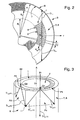
- FIG 3 schematically shows a simplified light ray representation of the formation of interference fringes in the photoresit layer 8 disposed on the circularly cylindrical surface 7 of the transparent cylinder 3.
- Each ray B1, respectively B2 of the incident beam impinging on the annular radial grating 1 forming the phase mask is diffracted at least in the transmitted -1 st and +1 st diffraction orders Tr- 1 (1) and Tr +1 (1), respectively Tr- 1 (2) and Tr +1 (2) in a geometrical plane P1, respectively P2 which is perpendicular to the grating line or groove at the incidence point Q1, respectively Q2.
- the angle between planes P1 and P2 depends on the radial position of the planar annular grating relative to the cylinder wall: the closer the planar grating to the cylinder wall, the larger the angle between P1 and P2.
- the transmitted -1 st and +1 st diffraction orders give rise to an interferogram having a given height along the direction of axis A and starting at a determined distance from the position of the phase mask grating on the cylinder axis.
- this interferogram occupies a given section of the circularly cylindrical surface 7 as shown in Figure 1 .
- the O th diffraction order does not impinge on the cylindrical surface 7 of the cylindrical element 3.
- Q1 and Q2 have both the same radial coordinate r and that all diffracted rays interfering in the photoresist layer initially have a same phase because the normally incident beam on the planar surface of the phase mask is formed by planar waves at least in the region of this phase mask.
- the azimuthal uniformity of the interferogram at the cylinder wall is ensured by the normally incident beam having a radial or an azimuthal polarization.
- the interferogram contrast q does not depend on the diffraction efficiency of the +1 st and -1 st orders of the phase mask grating, therefore q does not depend on the incident beam being radially or azimuthally polarized.
- the interference contrast depends on the angle between the two electric field vectors of the diffracted beams Tr +1 (1) and Tr -1 (2) : the contrast term q is zero if this angle is 90 degrees. Therefore, if the incident beam is radially polarized, the angle between OQ1 and OQ2 in Fig. 3 must not be close to 90 degrees. If the incident beam is azimuthally polarized, the angle ⁇ 1 must not be close to 45 degrees.
- the exposure of the photoresist layer 8 to the interferogram after development gives rise to a corrugation grating 9 in the photoresist layer of period ⁇ ⁇ R/2 as represented in perspective in Figure 1 .
- the lines and grooves of the grating transferred onto the cylindrical wall 7 are parallel to the axis A.
- An essentially sinusoidal corrugation profile results if the photoresist is set at its linear regime by uniform pre-exposure, and a binary corrugation profile results if the photoresist is set below threshold and exposed above saturation.
- the deposition of a uniform photoresist coating 8 on the cylinder wall is preferably made by dip-coating.
- the photoresist thickness is adjusted so as to prevent the creation of standing wave field nodes within the photoresist layer 8; this is the case if high reflection occurs at the air-photoresist interface in case the incidence angle of the +/-1 st orders at the cylindrical wall is large.
- the formation of a standing wave can be suppressed by immersing the cylinder in a liquid of refractive index close to n s , as for instance glycerol, which does not perturb the photochemistry of a standard positive photoresist.
- An index matching liquid will also be used in case of total internal reflection in the cylindrical element with air as the external medium.
- the photoresist layer 8 can be coated with an absorptive film of non-critical thickness such as an absorptive latex film to suppress the reflection at the photoresist-air interface.
- a number of processes can be used to obtain a cylindrical grating in hard material such as dry or wet etching of the element wall 7, or the electrochemical or electroless growth of a metal shim (nickel for instance) on the resist grating 9, followed in turn by a highly productive injection molding or UV- or hot-embossing process from a nickel shim or casting or extrusion.
- a metal shim nickel for instance
- a grating in hard material can also be obtained by a lift-off process whereby the developed photoresist grating 9 having its grooves preferably in the form of inverse trapezes is first coated by a metallic or dielectric layer, then the photoresist trapezes are chemically removed together with the layer material deposited on them, leaving lines of the deposited material where the resist grooves were.
- the exposure radiation is preferably narrow band and has a high spatial coherence such as that of a HeCd laser at 442 nm or 325 nm wavelength or a single transverse mode semiconductor laser at 406 nm wavelength.
- the normally incident beam B can cover the whole phase mask grating or a part of it which must be large enough to allow the interference of the -1 st and +1 st diffraction orders on the circularly cylindrical surface 7 of the cylinder element 3. i.e. in the photoresist layer 8.
- the beam B covers only a part of the phase mask grating, a high accuracy rotation of this beam around the central axis A is needed with possibly several turns to smooth the dose distribution across the stitching zone. Delivering the total exposure dose in the form of several turns with small dose permits to limit the dose jumps where the exposure began and where it ended.
- This exposure configuration is particularly advantageous for the writing of a cylindrical grating at the wall of a cylinder of large diameter, for instance as large as 300 mm where the radial phase mask grating 1 also has a large inner and outer diameter, for instance 293 and 298 nm respectively.
- the normally incident exposure beam diameter must be at least three times larger than the chord between the two intersection points at the cylinder wall of the +1 st and -1 st diffraction orders emanating from a single point of the phase mask grating, and the ring of the phase mask radial grating must be close to the cylinder wall.
- measures are taken to ensure an even power distribution in the photoresist layer 8 along the z axis by shaping the radial power distribution in the incident beam.
- the pattern of the phase mask grating 1 comprises radial lines 4 and grooves 5 of radially dependent widths w l and w g respectively. It is preferably a binary corrugation with essentially vertical walls.
- the pattern can be written by means of a laser or electron beam pattern generator in a photo- or electron-sensitive resist layer.
- a subsequent etching process transfers the resist grating pattern in the form of rectangular profile grooves into the element surface 2 at a depth t g or, as shown in a variant on figure 4 which will be described later, into and all through a high index layer 12 of refractive index n h and appropriate thickness t h deposited onto surface 2 of the cylinder 3, t h being also the depth of the grooves.
- the structure and profile of the phase mask grating can be chosen rather freely.
- the profile of the radial grating can be optimized for suppressing the second diffraction order.
- the grating of the phase mask can for instance simply be a binary corrugation in fused silica as in FBG (Fiber Bragg Grating) phase masks. It can also be a simple chromium mask grating on a glass or fused quartz substrate.
- the second transmitted orders propagate and form an interferogram at the wall of the cylinder. If this interferogram overlaps with the desired +1 st and -1 st order interferogram, the latter will be undesirably over-modulated by the former. However, there are ways to keep the diffraction efficiency of the second orders close to zero, for instance by adjusting the depth and duty cycle of a binary corrugation as this is currently made in FBG phase masks. If the period at the inner boundary of the ring forming the phase mask grating is larger than 3 ⁇ /ns, the third transmitted orders propagate.
- H m (r) the height of the phase mask center O on the cylinder axis A, at which the interferogram of m th order forms at the cylinder wall.
- H m r R 2 - r 2 1 / 2 ⁇ n s ⁇ ⁇ ⁇ ⁇ r / m ⁇ 2 - 1 1 / 2
- R is the cylinder radius
- r the radial coordinate in the phase mask grating ring
- ⁇ ⁇ is the angular period of the phase mask grating.
- the radially variable period of the phase mask grating 1 and the line/groove ratio can be produced by electron beam patterning with high precision and can be varied with high flexibility across the whole area of grating 1.
- the area of grating 1 can be composed of two or three sub-areas of concentric ring shape of the same angular period ⁇ ⁇ but predetermined angular shift corresponding to a prescribed fraction of the period ⁇ ⁇ . This results in two or three grating tracks on the cylindrical wall 7 of identical period but predetermined shift. This is an important characteristic of the disclosed grating writing method for the fabrication of rotation encoders where a first grating track delivers the sinus and a second grating track delivers the cosines of the rotation signal.
- N being an integer number larger than 1
- the corresponding shift in the phase mask grating 1 is a fraction 1/(2N) of a period.
- the radial phase mask grating can comprise a number of concentric sub-areas of different angular period which results on the cylindrical wall 7 in a number of cylindrical gratings of lines parallel to axis A and of different periods.
- the radial phase mask grating can be decomposed in a number of sections of identical azimuthal period with a phase shift between them in order to project on the cylinder wall 7 an interferogram having phase shifted sections. This is used for instance for having phase shifted grating sections in the same grating track on the cylinder.
- the interferogram does not have to be printed at the end surface of the very cylinder at the lateral surface of which the phase mask is micro-structured.
- FIG 4 higher productivity and more flexibility is gained by defining the phase mask 1 on a standalone disk or wafer 30.
- the cylinder 3 at the surface of which the interferogram is to be projected is placed concentrically with the stand alone phase mask support 30 which is arranged on or over the top face 2 of the cylinder 3, preferably with an index matching liquid film 33 in-between.
- the phase mask 1 can be placed at the bottom surface of the disk or wafer 30, at the side of the index matching fluid.
- the grating lines 4 of the phase mask grating 1 are preferably made of a high refractive index material such as Si 3 N 4 or Ta 2 0 5 or TiO 2 .
- the phase mask is formed by an index modulation within the disk or wafer 30 obtained for instance by ion implantation or by embedding a high index corrugation within a sandwich of two plates by wafer bonding method.
- the first embodiment concerns a fabrication method for a cylindrical grating at the convex wall 7 of a circular plate or rod by means of a radial phase mask grating defining a transmission grating.
- the same method can be used to project the interferogram onto the concave surface 17 of an element 13 having a circularly cylindrical surface 17 of inner radius R t surrounding a support 31 on which the annular phase mask is arranged concentrically to the circularly cylindrical surface 17, as illustrated in Figure 5 .
- the phase mask is a reflection grating.
- the support 31 is placed in or under a circularly cylindrical hole of the element 13.
- the photoresist layer 8 is spread at the inner wall 17 defined by the hole of the element 13.
- layer 6 is an absorptive or highly transmissive layer for the incident beam.
- an index matching liquid can be used between the support 31 or 30 and the circularly cylindrical surface 17 of the element 13 (e.g. a tube).
- An alternative to an exposure method applied to a concave wall is to make a negative replica of a cylindrical grating made on a convex cylinder 3 as initially described.
- This replica can be made in the form of a nickel shim grown on the convex photoresist grating followed by the dissolution of the resist grating and withdrawal or dissolution of the cylindrical element.
- the Ni-shim becomes the wanted concave grating.
- Higher productivity can be obtained by replicating this concave grating in the form of a nickel convex cylindrical grating, itself being replicated, possibly several times, to give rise to a number of replicated concave gratings.
- phase mask grating writing method can write a grating of period notably larger than the wavelength if R or R t is large without suffering from the presence of high diffraction orders since the phase mask grating generating the circularly cylindrical interferogram can be made to substantially diffract the +/-1 st orders only or to simply be placed at a small enough radius where the period does not diffract orders larger than 1.
- the photoresist coated wall onto which the interferogram is projected could also be a cone or any transparent body 34 of smooth surface of circular symmetry with a resist layer spread at its surface whose radius R co (z) has a linear or non-linear dependence on the axial coordinate z.
Landscapes
- Physics & Mathematics (AREA)
- General Physics & Mathematics (AREA)
- Engineering & Computer Science (AREA)
- Manufacturing & Machinery (AREA)
- Optics & Photonics (AREA)
- Diffracting Gratings Or Hologram Optical Elements (AREA)
Claims (9)
- Herstellungsverfahren eines zylindrischen Gitters an einer kreiszylindrischen Oberfläche (7; 17) eines Elements (3; 13), umfassend die folgenden Schritte:Vorsehen einer kreisförmigen Phasenblende, die durch ein ebenes radiales Beugungsgitter (1) gebildet ist;Beschichten der kreiszylindrischen Oberfläche (7; 17) mit einer lichtundurchlässigen Schicht (8);Anordnen der kreiszylindrischen Oberfläche (7; 17) relativ zu der kreisförmigen Phasenblende, wobei ein Medium bzw. Medien zwischen der kreisförmigen Phasenblende und der lichtundurchlässigen Schicht (8) auf der kreiszylindrischen Oberfläche (7; 17) zumindest für eine gegebene Wellenlänge transparent ist bzw. sind;Einstrahlen einer Lichtwelle auf die kreisförmige Phasenblende bei der gegebenen Wellenlänge, wobei das ebene radiale Beugungsgitter (1) eine ausgewählte Periode aufweist, so dass sich die +1-ste und -1-ste Beugungsordnungen (Tr+1; Tr-1) durch das Medium bzw. die Medien zwischen der kreisförmigen Phasenblende und der lichtundurchlässigen Schicht (8) ausbreiten und zu einem Interferogramm in der lichtundurchlässigen Schicht (8) führen; undAusbilden der lichtundurchlässigen Schicht (8) zu einem kreiszylinderförmigen lichtundurchlässigen Wellen-Beugungsgitter (9), das parallel zu einer Mittelachse (A) der kreiszylindrischen Oberfläche (7; 17) verlaufende Wellenlinien aufweist,dadurch gekennzeichnet, dassdie kreiszylindrische Oberfläche (7; 17) relativ zu der kreisförmigen Phasenblende derart angeordnet ist, dass die Mittelachse (A) ein Zentrum (O) der kreisförmigen Phasenblende miteinschließt, so dass die Mittelachse (A) im Wesentlichen senkrecht zu dem ebenen radialen Beugungsgitter (1) ist, unddie kreisförmige Phasenblende mit der Lichtwelle im Wesentlichen unter senkrechtem Einfall belichtet ist, so dass die 0-te Beugungsordnung als ein im Wesentlichen kollimierter Strahl (B) verbleibt, der sich in Richtung der Mittelachse (A) der kreiszylindrischen Oberfläche (7; 17) ausbreitet.
- Herstellungsverfahren nach Anspruch 1, dadurch gekennzeichnet, dass die kreisförmige Phasenblende eine Phasenübertragungsblende ist, die direkt an einer Stirnfläche (2) des Elements (3) angeordnet ist, das transparent für die gegebene Wellenlänge ist.
- Herstellungsverfahren nach Anspruch 1, dadurch gekennzeichnet, dass die kreisförmige Phasenblende eine Phasenübertragungsblende ist, die auf, unter oder in einer eigenständigen Platte oder Halbleiterscheibe (30) angeordnet ist, die relativ zu dem Element (3) angeordnet ist, so dass das Interferogramm in einem bestimmten Abschnitt der kreiszylindrischen Oberfläche (7; 17) des Elements (3) entsteht, wobei die Platte oder Halbleiterscheibe (30) für die gegebene Wellenlänge transparent ist.
- Herstellungsverfahren nach Anspruch 2 oder 3, dadurch gekennzeichnet, dass eine Schicht (6) auf einem Bereich außerhalb der kreisförmigen Phasenblende aufgetragen ist, wobei die Schicht (6) absorbierend oder reflektierend für die vorgegebene Wellenlänge ist.
- Herstellungsverfahren nach Anspruch 1, dadurch gekennzeichnet, dass die kreisförmige Phasenblende eine Reflexionsphasenblende ist, die auf, unter oder in einer eigenständigen Platte oder Halbleiterscheibe (30) angeordnet ist, die relativ zu dem Element (3) angeordnet ist, so dass das Interferogramm in einem bestimmten Abschnitt der kreiszylindrischen Oberfläche (7; 17) des Elements (3) entsteht.
- Herstellungsverfahren nach Anspruch 5, dadurch gekennzeichnet, dass eine Schicht (6) auf einem Bereich außerhalb der kreisförmigen Phasenblende aufgetragen ist, wobei die Schicht (6) absorbierend oder lichtdurchlässig für die vorgegebene Wellenlänge ist.
- Herstellungsverfahren nach einem der Ansprüche 1 bis 6, dadurch gekennzeichnet, dass die kreiszylindrische Oberfläche (7) konvex ist und eine Außenwand des Elementes (3) definiert.
- Herstellungsverfahren nach einem der Ansprüche 1 bis 6, dadurch gekennzeichnet, dass die kreiszylindrische Oberfläche (7) konkav ist und eine Innenwand des Elementes (3) definiert.
- Herstellungsverfahren nach einem der Ansprüche 1 bis 8, gekennzeichnet durch einen letzten Schritt, der in Formen des zylindrischen Beugungsgitters durch physikalisches Umdrucken oder Prägen oder Spritzgießen oder Extrudieren der kreiszylinderförmigen lichtundurchlässigen Wellen-Beugungsgitter (9) besteht.
Priority Applications (2)
| Application Number | Priority Date | Filing Date | Title |
|---|---|---|---|
| EP11290380.2A EP2562568B1 (de) | 2011-08-23 | 2011-08-23 | Herstellungsverfahren von zylindrischen Gittern |
| US13/443,443 US8586287B2 (en) | 2011-08-23 | 2012-04-10 | Fabrication method of cylindrical gratings |
Applications Claiming Priority (1)
| Application Number | Priority Date | Filing Date | Title |
|---|---|---|---|
| EP11290380.2A EP2562568B1 (de) | 2011-08-23 | 2011-08-23 | Herstellungsverfahren von zylindrischen Gittern |
Publications (2)
| Publication Number | Publication Date |
|---|---|
| EP2562568A1 EP2562568A1 (de) | 2013-02-27 |
| EP2562568B1 true EP2562568B1 (de) | 2014-06-25 |
Family
ID=44674656
Family Applications (1)
| Application Number | Title | Priority Date | Filing Date |
|---|---|---|---|
| EP11290380.2A Not-in-force EP2562568B1 (de) | 2011-08-23 | 2011-08-23 | Herstellungsverfahren von zylindrischen Gittern |
Country Status (2)
| Country | Link |
|---|---|
| US (1) | US8586287B2 (de) |
| EP (1) | EP2562568B1 (de) |
Families Citing this family (13)
| Publication number | Priority date | Publication date | Assignee | Title |
|---|---|---|---|---|
| JP6158213B2 (ja) * | 2012-11-19 | 2017-07-05 | 日立コンシューマエレクトロニクス株式会社 | 光情報記録装置、光情報記録再生装置、光情報記録方法、光情報記録再生方法、及び光学素子 |
| UA123038C2 (uk) * | 2014-05-22 | 2021-02-10 | Аустреліан Нуклеар Саєнс Енд Текнолоджі Органісейшн | Візуалізація гамма-випромінювання |
| JP6882316B2 (ja) * | 2016-03-04 | 2021-06-02 | アプライド マテリアルズ インコーポレイテッドApplied Materials,Incorporated | ワイヤグリッド偏光板製造方法 |
| EP3516328B1 (de) * | 2016-09-21 | 2023-05-03 | Philip M. Johnson | Kontaktlose koordinatenmessmaschine mit hybridem cyclischem binär-codiertem strukturierten licht |
| US10295648B2 (en) | 2017-06-29 | 2019-05-21 | Mitutoyo Corporation | Contamination and defect resistant optical encoder configuration including a normal of readhead plane at a non-zero pitch angle relative to measuring axis for providing displacement signals |
| US10295378B2 (en) | 2017-06-29 | 2019-05-21 | Mitutoyo Corporation | Contamination and defect resistant optical encoder configuration outputting structured illumination to a scale plane for providing displacement signals |
| US10302466B2 (en) | 2017-06-29 | 2019-05-28 | Mitutoyo Corporation | Contamination and defect resistant optical encoder configuration including first and second illumination source diffraction gratings arranged in first and second parallel planes for providing displacement signals |
| US10648838B2 (en) | 2017-06-29 | 2020-05-12 | Mitutoyo Corporation | Contamination and defect resistant rotary optical encoder configuration including a rotary scale with yawed scale grating bars and structured illumination generating arrangement with a beam deflector configuration |
| US10502593B1 (en) * | 2018-06-07 | 2019-12-10 | Philip M. Johnson | Linear and rotary multitrack absolute position encoder and methods using the same |
| CN109974628B (zh) * | 2019-04-09 | 2020-09-01 | 合肥工业大学 | 一种基于误差源分析的圆光栅传感器测角误差修正方法 |
| CN114514443A (zh) * | 2019-07-19 | 2022-05-17 | 奇跃公司 | 制造衍射光栅的方法 |
| CN112799162B (zh) * | 2021-02-02 | 2024-11-08 | 廊坊市莱格光电仪器有限公司 | 一种激光直刻金属柱面光栅光刻机 |
| CN116964493A (zh) * | 2021-03-08 | 2023-10-27 | 特拉克森股份有限公司 | 圆柱形体介质中的体布拉格光栅 |
Family Cites Families (8)
| Publication number | Priority date | Publication date | Assignee | Title |
|---|---|---|---|---|
| JPH05312594A (ja) * | 1992-05-08 | 1993-11-22 | Ricoh Co Ltd | 格子作製方法 |
| JP3478567B2 (ja) | 1992-09-25 | 2003-12-15 | キヤノン株式会社 | 回転情報検出装置 |
| JPH07146405A (ja) | 1993-11-24 | 1995-06-06 | Shimadzu Corp | レプリカ回折格子 |
| JP3935941B2 (ja) | 1996-01-16 | 2007-06-27 | ブリティッシュ・テレコミュニケーションズ・パブリック・リミテッド・カンパニー | 光媒体内に屈折率パターンを記録するための方法及び装置 |
| JP2001520395A (ja) | 1997-10-17 | 2001-10-30 | ビショップ イノヴェーション リミテッド | 光学トルクトランスデュサーの製造方法 |
| US6344298B1 (en) * | 1999-08-26 | 2002-02-05 | Sabeus Photonics, Inc. | Circumferentially varying mask and fabrication of fiber gratings using a mask |
| EP1462831B1 (de) * | 2003-03-21 | 2008-05-14 | Her Majesty in Right of Canada as Represented by the Minister of Industry | Bragg-Gitter und dazugehörige Herstellungsmethode, die einen ultraschnellen Laser verwendet |
| EP2367058A1 (de) * | 2010-03-17 | 2011-09-21 | Université Jean-Monnet | Herstellungsverfahren von zylindrischen Gittern |
-
2011
- 2011-08-23 EP EP11290380.2A patent/EP2562568B1/de not_active Not-in-force
-
2012
- 2012-04-10 US US13/443,443 patent/US8586287B2/en not_active Expired - Fee Related
Also Published As
| Publication number | Publication date |
|---|---|
| EP2562568A1 (de) | 2013-02-27 |
| US20130052592A1 (en) | 2013-02-28 |
| US8586287B2 (en) | 2013-11-19 |
Similar Documents
| Publication | Publication Date | Title |
|---|---|---|
| EP2562568B1 (de) | Herstellungsverfahren von zylindrischen Gittern | |
| AU731744B2 (en) | Phase mask with spatially variable diffraction efficiency | |
| EP2367058A1 (de) | Herstellungsverfahren von zylindrischen Gittern | |
| EP0684491B1 (de) | Verfahren zur Herstellung eines Bragg Gitters in einem fotoempfindlichen optischen Wellenleiter | |
| US9036133B2 (en) | Lithographic fabrication of general periodic structures by exposing a photosensitive layer to a range of lateral intensity distributions | |
| US20140126029A1 (en) | Method and device for the layered production of thin volume grid stacks, and beam combiner for a holographic display | |
| US8221963B2 (en) | Method for producing fine structure | |
| Zang et al. | High-precision two-dimensional displacement metrology based on matrix metasurface | |
| US20040032667A1 (en) | Technique for microstructuring replication mold | |
| US20070249072A1 (en) | Method and apparatus for producing interferometric lithography patterns with circular symmetry | |
| JP5391670B2 (ja) | 微細構造体の製造方法 | |
| Shimizu et al. | Design optimization of a non-orthogonal two-axis Lloyd's mirror interferometer for fabrication of large-area two-dimensional scale gratings | |
| Zhang et al. | Distance and depth modulation of Talbot imaging via specified design of the grating structure | |
| US11687004B2 (en) | System and method for industrial scale continuous holographic lithography | |
| Burmeister et al. | CGH for ESO’s ELT M2 reference plate: fabrication of high precision CGHs | |
| Solak et al. | Patterning of circular structure arrays with interference lithography | |
| Tonchev et al. | Subwavelength cylindrical grating by holistic phase-mask coordinate transform | |
| Poleshchuk | Fabrication and application of diffractive optical elements | |
| CN113946008A (zh) | 一种相位和振幅联合调制的复合波带片 | |
| LI et al. | 42000 Saint Etienne Cedex 2 (FR) | |
| JPH05346503A (ja) | ゾーンプレートの製造方法 | |
| Park et al. | Full-size lamellar grating for the cosmic beamline at ALS-U | |
| CN101191855A (zh) | “之”字形衍射光栅 | |
| JP2006284960A (ja) | 回折格子、回折格子の製造方法、該回折格子を用いる露光方法、電子デバイス製造方法、電子デバイスおよび露光装置 | |
| Zherdev et al. | Adjustment of Phase Shift of Measurement Signals in an Optical Encoder from the Parameters of an Analyzing Scale |
Legal Events
| Date | Code | Title | Description |
|---|---|---|---|
| PUAI | Public reference made under article 153(3) epc to a published international application that has entered the european phase |
Free format text: ORIGINAL CODE: 0009012 |
|
| AK | Designated contracting states |
Kind code of ref document: A1 Designated state(s): AL AT BE BG CH CY CZ DE DK EE ES FI FR GB GR HR HU IE IS IT LI LT LU LV MC MK MT NL NO PL PT RO RS SE SI SK SM TR |
|
| AX | Request for extension of the european patent |
Extension state: BA ME |
|
| 17P | Request for examination filed |
Effective date: 20130819 |
|
| RBV | Designated contracting states (corrected) |
Designated state(s): AL AT BE BG CH CY CZ DE DK EE ES FI FR GB GR HR HU IE IS IT LI LT LU LV MC MK MT NL NO PL PT RO RS SE SI SK SM TR |
|
| RAP1 | Party data changed (applicant data changed or rights of an application transferred) |
Owner name: SICK STEGMANN GMBH |
|
| 17Q | First examination report despatched |
Effective date: 20131113 |
|
| GRAP | Despatch of communication of intention to grant a patent |
Free format text: ORIGINAL CODE: EPIDOSNIGR1 |
|
| RIC1 | Information provided on ipc code assigned before grant |
Ipc: G03F 1/60 20120101ALI20140227BHEP Ipc: G02B 5/18 20060101AFI20140227BHEP Ipc: G03F 7/24 20060101ALI20140227BHEP Ipc: G03F 7/20 20060101ALI20140227BHEP |
|
| INTG | Intention to grant announced |
Effective date: 20140325 |
|
| RIN1 | Information on inventor provided before grant (corrected) |
Inventor name: PARRIAUX, OLIVIER Inventor name: TONCHEV, SWETLEN |
|
| GRAS | Grant fee paid |
Free format text: ORIGINAL CODE: EPIDOSNIGR3 |
|
| GRAA | (expected) grant |
Free format text: ORIGINAL CODE: 0009210 |
|
| AK | Designated contracting states |
Kind code of ref document: B1 Designated state(s): AL AT BE BG CH CY CZ DE DK EE ES FI FR GB GR HR HU IE IS IT LI LT LU LV MC MK MT NL NO PL PT RO RS SE SI SK SM TR |
|
| REG | Reference to a national code |
Ref country code: GB Ref legal event code: FG4D |
|
| REG | Reference to a national code |
Ref country code: CH Ref legal event code: EP |
|
| REG | Reference to a national code |
Ref country code: AT Ref legal event code: REF Ref document number: 675018 Country of ref document: AT Kind code of ref document: T Effective date: 20140715 |
|
| REG | Reference to a national code |
Ref country code: IE Ref legal event code: FG4D |
|
| REG | Reference to a national code |
Ref country code: DE Ref legal event code: R096 Ref document number: 602011007920 Country of ref document: DE Effective date: 20140807 |
|
| PG25 | Lapsed in a contracting state [announced via postgrant information from national office to epo] |
Ref country code: FI Free format text: LAPSE BECAUSE OF FAILURE TO SUBMIT A TRANSLATION OF THE DESCRIPTION OR TO PAY THE FEE WITHIN THE PRESCRIBED TIME-LIMIT Effective date: 20140625 Ref country code: LT Free format text: LAPSE BECAUSE OF FAILURE TO SUBMIT A TRANSLATION OF THE DESCRIPTION OR TO PAY THE FEE WITHIN THE PRESCRIBED TIME-LIMIT Effective date: 20140625 Ref country code: NO Free format text: LAPSE BECAUSE OF FAILURE TO SUBMIT A TRANSLATION OF THE DESCRIPTION OR TO PAY THE FEE WITHIN THE PRESCRIBED TIME-LIMIT Effective date: 20140925 Ref country code: GR Free format text: LAPSE BECAUSE OF FAILURE TO SUBMIT A TRANSLATION OF THE DESCRIPTION OR TO PAY THE FEE WITHIN THE PRESCRIBED TIME-LIMIT Effective date: 20140926 Ref country code: CY Free format text: LAPSE BECAUSE OF FAILURE TO SUBMIT A TRANSLATION OF THE DESCRIPTION OR TO PAY THE FEE WITHIN THE PRESCRIBED TIME-LIMIT Effective date: 20140625 |
|
| REG | Reference to a national code |
Ref country code: AT Ref legal event code: MK05 Ref document number: 675018 Country of ref document: AT Kind code of ref document: T Effective date: 20140625 |
|
| REG | Reference to a national code |
Ref country code: NL Ref legal event code: VDEP Effective date: 20140625 |
|
| REG | Reference to a national code |
Ref country code: LT Ref legal event code: MG4D |
|
| PG25 | Lapsed in a contracting state [announced via postgrant information from national office to epo] |
Ref country code: HR Free format text: LAPSE BECAUSE OF FAILURE TO SUBMIT A TRANSLATION OF THE DESCRIPTION OR TO PAY THE FEE WITHIN THE PRESCRIBED TIME-LIMIT Effective date: 20140625 Ref country code: SE Free format text: LAPSE BECAUSE OF FAILURE TO SUBMIT A TRANSLATION OF THE DESCRIPTION OR TO PAY THE FEE WITHIN THE PRESCRIBED TIME-LIMIT Effective date: 20140625 Ref country code: LV Free format text: LAPSE BECAUSE OF FAILURE TO SUBMIT A TRANSLATION OF THE DESCRIPTION OR TO PAY THE FEE WITHIN THE PRESCRIBED TIME-LIMIT Effective date: 20140625 Ref country code: RS Free format text: LAPSE BECAUSE OF FAILURE TO SUBMIT A TRANSLATION OF THE DESCRIPTION OR TO PAY THE FEE WITHIN THE PRESCRIBED TIME-LIMIT Effective date: 20140625 |
|
| PG25 | Lapsed in a contracting state [announced via postgrant information from national office to epo] |
Ref country code: EE Free format text: LAPSE BECAUSE OF FAILURE TO SUBMIT A TRANSLATION OF THE DESCRIPTION OR TO PAY THE FEE WITHIN THE PRESCRIBED TIME-LIMIT Effective date: 20140625 Ref country code: RO Free format text: LAPSE BECAUSE OF FAILURE TO SUBMIT A TRANSLATION OF THE DESCRIPTION OR TO PAY THE FEE WITHIN THE PRESCRIBED TIME-LIMIT Effective date: 20140625 Ref country code: PT Free format text: LAPSE BECAUSE OF FAILURE TO SUBMIT A TRANSLATION OF THE DESCRIPTION OR TO PAY THE FEE WITHIN THE PRESCRIBED TIME-LIMIT Effective date: 20141027 Ref country code: CZ Free format text: LAPSE BECAUSE OF FAILURE TO SUBMIT A TRANSLATION OF THE DESCRIPTION OR TO PAY THE FEE WITHIN THE PRESCRIBED TIME-LIMIT Effective date: 20140625 Ref country code: SK Free format text: LAPSE BECAUSE OF FAILURE TO SUBMIT A TRANSLATION OF THE DESCRIPTION OR TO PAY THE FEE WITHIN THE PRESCRIBED TIME-LIMIT Effective date: 20140625 Ref country code: ES Free format text: LAPSE BECAUSE OF FAILURE TO SUBMIT A TRANSLATION OF THE DESCRIPTION OR TO PAY THE FEE WITHIN THE PRESCRIBED TIME-LIMIT Effective date: 20140625 |
|
| PG25 | Lapsed in a contracting state [announced via postgrant information from national office to epo] |
Ref country code: AT Free format text: LAPSE BECAUSE OF FAILURE TO SUBMIT A TRANSLATION OF THE DESCRIPTION OR TO PAY THE FEE WITHIN THE PRESCRIBED TIME-LIMIT Effective date: 20140625 Ref country code: PL Free format text: LAPSE BECAUSE OF FAILURE TO SUBMIT A TRANSLATION OF THE DESCRIPTION OR TO PAY THE FEE WITHIN THE PRESCRIBED TIME-LIMIT Effective date: 20140625 Ref country code: IS Free format text: LAPSE BECAUSE OF FAILURE TO SUBMIT A TRANSLATION OF THE DESCRIPTION OR TO PAY THE FEE WITHIN THE PRESCRIBED TIME-LIMIT Effective date: 20141025 Ref country code: NL Free format text: LAPSE BECAUSE OF FAILURE TO SUBMIT A TRANSLATION OF THE DESCRIPTION OR TO PAY THE FEE WITHIN THE PRESCRIBED TIME-LIMIT Effective date: 20140625 |
|
| REG | Reference to a national code |
Ref country code: DE Ref legal event code: R097 Ref document number: 602011007920 Country of ref document: DE |
|
| PG25 | Lapsed in a contracting state [announced via postgrant information from national office to epo] |
Ref country code: LU Free format text: LAPSE BECAUSE OF FAILURE TO SUBMIT A TRANSLATION OF THE DESCRIPTION OR TO PAY THE FEE WITHIN THE PRESCRIBED TIME-LIMIT Effective date: 20140823 Ref country code: MC Free format text: LAPSE BECAUSE OF FAILURE TO SUBMIT A TRANSLATION OF THE DESCRIPTION OR TO PAY THE FEE WITHIN THE PRESCRIBED TIME-LIMIT Effective date: 20140625 |
|
| REG | Reference to a national code |
Ref country code: CH Ref legal event code: PL |
|
| PG25 | Lapsed in a contracting state [announced via postgrant information from national office to epo] |
Ref country code: BE Free format text: LAPSE BECAUSE OF NON-PAYMENT OF DUE FEES Effective date: 20140831 Ref country code: LI Free format text: LAPSE BECAUSE OF NON-PAYMENT OF DUE FEES Effective date: 20140831 Ref country code: CH Free format text: LAPSE BECAUSE OF NON-PAYMENT OF DUE FEES Effective date: 20140831 Ref country code: DK Free format text: LAPSE BECAUSE OF FAILURE TO SUBMIT A TRANSLATION OF THE DESCRIPTION OR TO PAY THE FEE WITHIN THE PRESCRIBED TIME-LIMIT Effective date: 20140625 Ref country code: IT Free format text: LAPSE BECAUSE OF FAILURE TO SUBMIT A TRANSLATION OF THE DESCRIPTION OR TO PAY THE FEE WITHIN THE PRESCRIBED TIME-LIMIT Effective date: 20140625 |
|
| PLBE | No opposition filed within time limit |
Free format text: ORIGINAL CODE: 0009261 |
|
| STAA | Information on the status of an ep patent application or granted ep patent |
Free format text: STATUS: NO OPPOSITION FILED WITHIN TIME LIMIT |
|
| REG | Reference to a national code |
Ref country code: IE Ref legal event code: MM4A |
|
| REG | Reference to a national code |
Ref country code: FR Ref legal event code: ST Effective date: 20150430 |
|
| 26N | No opposition filed |
Effective date: 20150326 |
|
| PG25 | Lapsed in a contracting state [announced via postgrant information from national office to epo] |
Ref country code: BE Free format text: LAPSE BECAUSE OF FAILURE TO SUBMIT A TRANSLATION OF THE DESCRIPTION OR TO PAY THE FEE WITHIN THE PRESCRIBED TIME-LIMIT Effective date: 20140625 |
|
| PG25 | Lapsed in a contracting state [announced via postgrant information from national office to epo] |
Ref country code: FR Free format text: LAPSE BECAUSE OF NON-PAYMENT OF DUE FEES Effective date: 20140901 Ref country code: IE Free format text: LAPSE BECAUSE OF NON-PAYMENT OF DUE FEES Effective date: 20140823 |
|
| PG25 | Lapsed in a contracting state [announced via postgrant information from national office to epo] |
Ref country code: SI Free format text: LAPSE BECAUSE OF FAILURE TO SUBMIT A TRANSLATION OF THE DESCRIPTION OR TO PAY THE FEE WITHIN THE PRESCRIBED TIME-LIMIT Effective date: 20140625 |
|
| GBPC | Gb: european patent ceased through non-payment of renewal fee |
Effective date: 20150823 |
|
| PG25 | Lapsed in a contracting state [announced via postgrant information from national office to epo] |
Ref country code: SM Free format text: LAPSE BECAUSE OF FAILURE TO SUBMIT A TRANSLATION OF THE DESCRIPTION OR TO PAY THE FEE WITHIN THE PRESCRIBED TIME-LIMIT Effective date: 20140625 |
|
| PG25 | Lapsed in a contracting state [announced via postgrant information from national office to epo] |
Ref country code: BG Free format text: LAPSE BECAUSE OF FAILURE TO SUBMIT A TRANSLATION OF THE DESCRIPTION OR TO PAY THE FEE WITHIN THE PRESCRIBED TIME-LIMIT Effective date: 20140625 Ref country code: MT Free format text: LAPSE BECAUSE OF FAILURE TO SUBMIT A TRANSLATION OF THE DESCRIPTION OR TO PAY THE FEE WITHIN THE PRESCRIBED TIME-LIMIT Effective date: 20140625 |
|
| PG25 | Lapsed in a contracting state [announced via postgrant information from national office to epo] |
Ref country code: GB Free format text: LAPSE BECAUSE OF NON-PAYMENT OF DUE FEES Effective date: 20150823 Ref country code: TR Free format text: LAPSE BECAUSE OF FAILURE TO SUBMIT A TRANSLATION OF THE DESCRIPTION OR TO PAY THE FEE WITHIN THE PRESCRIBED TIME-LIMIT Effective date: 20140625 Ref country code: HU Free format text: LAPSE BECAUSE OF FAILURE TO SUBMIT A TRANSLATION OF THE DESCRIPTION OR TO PAY THE FEE WITHIN THE PRESCRIBED TIME-LIMIT; INVALID AB INITIO Effective date: 20110823 |
|
| PG25 | Lapsed in a contracting state [announced via postgrant information from national office to epo] |
Ref country code: MK Free format text: LAPSE BECAUSE OF FAILURE TO SUBMIT A TRANSLATION OF THE DESCRIPTION OR TO PAY THE FEE WITHIN THE PRESCRIBED TIME-LIMIT Effective date: 20140625 |
|
| PG25 | Lapsed in a contracting state [announced via postgrant information from national office to epo] |
Ref country code: AL Free format text: LAPSE BECAUSE OF FAILURE TO SUBMIT A TRANSLATION OF THE DESCRIPTION OR TO PAY THE FEE WITHIN THE PRESCRIBED TIME-LIMIT Effective date: 20140625 |
|
| REG | Reference to a national code |
Ref country code: DE Ref legal event code: R082 Ref document number: 602011007920 Country of ref document: DE Ref country code: DE Ref legal event code: R081 Ref document number: 602011007920 Country of ref document: DE Owner name: SICK AG, DE Free format text: FORMER OWNER: SICK STEGMANN GMBH, 78166 DONAUESCHINGEN, DE |
|
| PGFP | Annual fee paid to national office [announced via postgrant information from national office to epo] |
Ref country code: DE Payment date: 20210819 Year of fee payment: 11 |
|
| REG | Reference to a national code |
Ref country code: DE Ref legal event code: R119 Ref document number: 602011007920 Country of ref document: DE |
|
| PG25 | Lapsed in a contracting state [announced via postgrant information from national office to epo] |
Ref country code: DE Free format text: LAPSE BECAUSE OF NON-PAYMENT OF DUE FEES Effective date: 20230301 |